RF LDMOS Wideband Integrated
Power Amplifiers
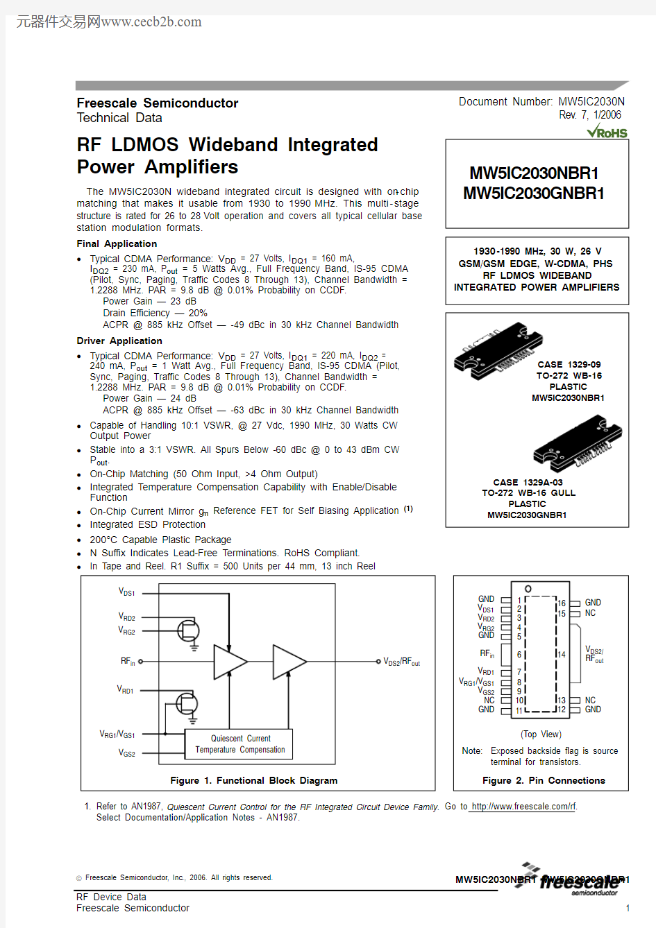
The MW5IC2030N wideband integrated circuit is designed with on-chip
matching that makes it usable from 1930 to 1990MHz. This multi-stage
structure is rated for 26 to 28Volt operation and covers all typical cellular base
station modulation formats.
Final Application
?Typical CDMA Performance: V DD = 27 Volts, I DQ1 = 160 mA,
I DQ2 = 230 mA, P out = 5 Watts Avg., Full Frequency Band, IS-95 CDMA
(Pilot, Sync, Paging, Traffic Codes 8 Through 13), Channel Bandwidth =
1.2288 MHz. PAR = 9.8 dB @ 0.01% Probability on CCDF.
Power Gain — 23 dB
Drain Efficiency — 20%
ACPR @ 885 kHz Offset — -49 dBc in 30 kHz Channel Bandwidth
Driver Application
?Typical CDMA Performance: V DD = 27 Volts, I DQ1 = 220 mA, I DQ2 =
240 mA, P out = 1 Watt Avg., Full Frequency Band, IS-95 CDMA (Pilot,
Sync, Paging, Traffic Codes 8 Through 13), Channel Bandwidth =
1.2288 MHz. PAR = 9.8 dB @ 0.01% Probability on CCDF.
Power Gain — 24 dB
ACPR @ 885 kHz Offset — -63 dBc in 30 kHz Channel Bandwidth
?Capable of Handling 10:1 VSWR, @ 27 Vdc, 1990 MHz, 30 Watts CW
Output Power
?Stable into a 3:1 VSWR. All Spurs Below -60 dBc @ 0 to 43 dBm CW
P out.
?On-Chip Matching (50 Ohm Input, >4 Ohm Output)
?Integrated Temperature Compensation Capability with Enable/Disable
Function
?On-Chip Current Mirror g m Reference FET for Self Biasing Application (1)
?Integrated ESD Protection
?200°C Capable Plastic Package
?N Suffix Indicates Lead-Free Terminations. RoHS Compliant.
?In Tape and Reel. R1 Suffix = 500 Units per 44 mm, 13 inch Reel
1.Refer to AN1987, Quiescent Current Control for the RF Integrated Circuit Device Family. Go to https://www.doczj.com/doc/3918696928.html,/rf.
Select Documentation/Application Notes - AN1987.
Document Number: MW5IC2030N
Rev. 7, 1/2006 Freescale Semiconductor
Technical Data
MW5IC2030NBR1
MW5IC2030GNBR1
2
RF Device Data
Freescale Semiconductor
MW5IC2030NBR1 MW5IC2030GNBR1Table 1. Maximum Ratings
Rating
Symbol Value Unit Drain-Source Voltage V DSS -0.5, +65Vdc Gate-Source Voltage V GS -0.5, +15Vdc Storage Temperature Range T stg -65 to +175
°C Operating Junction Temperature T J 200°C Input Power
P in
20
dBm
Table 2. Thermal Characteristics
Characteristic
Symbol Value (1,2)
Unit Thermal Resistance, Junction to Case CDMA Application Stage 1, 27 Vdc, I DQ = 160 mA (P out = 5 W CW)Stage 2, 27 Vdc, I DQ = 230 mA PHS Application Stage 1, 26 Vdc, I DQ = 300 mA (P out = 12.6 W CW)
Stage 2, 26 Vdc, I DQ = 1300 mA
R θJC
4.891.754.851.61°C/W
Table 3. ESD Protection Characteristics
Test Conditions
Class Human Body Model 1B (Minimum)Machine Model A (Minimum)Charge Device Model
3 (Minimum)
Table 4. Moisture Sensitivity Level
Test Methodology
Rating Package Peak Temperature
Unit Per JESD 22-A113, IPC/JEDEC J-STD-020
3
260
°C
Table 5. Electrical Characteristics (T C = 25°C unless otherwise noted)
Characteristic
Symbol
Min
Typ
Max
Unit
CDMA Functional Tests (In Freescale 1900 MHz Test Fixture, 50 οhm system) V DD = 27 Vdc, I DQ1 = 160 mA, I DQ2 = 230 mA, P out = 5 W Avg., 1960 MHz, Single-Carrier N-CDMA, 1.2288 MHz Channel Bandwidth Carrier. ACPR measured in 30 kHz Channel Bandwidth @ ± 885 kHz Offset. PAR = 9.8 dB @ 0.01 Probability on CCDF.Power Gain G ps 21.523—dB Drain Efficiency ηD 1820—%Input Return Loss
IRL —-18-10dB Adjacent Channel Power Ratio
ACPR —-49-47dBc Gain Flatness in 30 MHz BW, 1930-1990 MHz
G F
—
0.2
0.3
dB
1.MTTF calculator available at https://www.doczj.com/doc/3918696928.html,/rf. Select Tools/Software/Application Software/Calculators to access the MTTF calculators by product.
2.Refer to AN1955, Thermal Measurement Methodology of RF Power Amplifiers. Go to https://www.doczj.com/doc/3918696928.html,/rf. Select Documentation/Application Notes - AN1955.
(continued)
MW5IC2030NBR1 MW5IC2030GNBR1
3
RF Device Data
Freescale Semiconductor
Table 5. Electrical Characteristics (T C = 25°C unless otherwise noted) (continued)
Characteristic
Symbol Min Typ Max Unit Typical Performances (In Freescale Test Fixture) V DD = 26 Vdc, I DQ1 = 160 mA, I DQ2 = 230 mA, P out = 5 W, f = 1960 MHz
P out @ 1 dB Compression Point, CW P1dB —30—W Deviation from Linear Phase in 30 MHz BW (Characterized from 1930-1990 MHz)Φ—±1—°Delay
Delay — 2.25—ns Part-to-Part Phase Variation
?Φ—±10—°Part-to-Part Gain Variation (Per Lot or Reel)
?G
—±1.5—dB Reference FET to RF FET Scaling Ratio Delta (Stages 1 and 2)
—
10
—
%
Typical PHS Performances (In Freescale Test Fixture, 50 οhm system) V DD = 26 Vdc, I DQ1 = 260 mA, I DQ2 = 1100 mA, P out = 12.6 W, 1900 MHz, PHS Signal Mask Power Gain G ps —24—dB Drain Efficiency ηD —25—%Input Return Loss
IRL —-15—dB Adjacent Channel Power Ratio (600 kHz Offset in 192 kHz BW)
ACPR
—
-72
—
dBc
4
RF Device Data
Freescale Semiconductor
MW5IC2030NBR1 MW5IC2030GNBR1
Figure 3. MW5IC2030NBR1(GNBR1) Test Circuit Schematic
Z70.200″ x 0.025″Microstrip Z80.274″ x 0.050″Microstrip Z90.615″ x 0.050″Microstrip Z100.450″ x 0.025″Microstrip Z110.340″ x 0.014″Microstrip PCB
Rogers 4350, 0.020″, εr = 3.5
Z10.465″ x 0.041″Microstrip Z20.518″ x 0.041″Microstrip Z30.282″ x 0.235″Microstrip Z40.221″ x 0.081″Microstrip Z50.489″ x 0.041″Microstrip Z60.471″ x 0.025″Microstrip Table 6. MW5IC2030NBR1(GNBR1) Test Circuit Component Designations and Values
Part
Description
Part Number Manufacturer C1 1.8 pF High Q Chip Capacitor (0603)600S1R8AT-250-T ATC C2 1.5 pF High Q Chip Capacitor (0603)600S1R5AT-250-T ATC C3 3.9 pF High Q Chip Capacitor (0603)600S3R9AT-250-T ATC C4 6.8 pF High Q Chip Capacitor (0805)600S6R8AT-250-T ATC C5, C6100 pF Class 1 NPO Chip Capacitors (0805)GRM215CB1H101CZ01D Murata C7
4.7 pF Class 1 NPO Chip Capacitor (0805)GRM215CB1H4R7CZ01D Murata C8, C9, C10, C110.1 μF X7R Chip Capacitors (1206)
C1206C104K5RACT Kemet C12, C13, C14, C15, C160.01 μF Class 2 X7R Chip Capacitors (0805)C0805C103K5RACT Kemet C17, C1822 μF, 35 V Electrolytic Capacitors ECE-1AVKS220Panasonic C19, C20330 μF, 50 V Electrolytic Capacitors ECA-1HM331
Panasonic
R1, R3 1 k W , 5% Chip Resistors (0805)R2499 W , 1% Chip Resistor (0805)R4, R5, R6
100 k W , 5% Chip Resistors (0805)
MW5IC2030NBR1 MW5IC2030GNBR1
5
RF Device Data
Freescale Semiconductor
Figure 4. MW5IC2030NBR1(GNBR1) Test Circuit Component Layout
Freescale has begun the transition of marking Printed Circuit Boards (PCBs) with the Freescale Semiconductor signature/logo. PCBs may have either Motorola or Freescale markings during the transition period. These changes will have no impact on form, fit or function of the current product.
6
RF Device Data
Freescale Semiconductor
MW5IC2030NBR1 MW5IC2030GNBR1TYPICAL CHARACTERISTICS
100
1926
0.1P out , OUTPUT POWER (WATTS) PEP Figure 7. Two-Tone Power Gain versus
Output Power G p s , P O W E R G A I N (d B )
2524232221
201
10100
0.1P out , OUTPUT POWER (WATTS) PEP
1
10Figure 8. Intermodulation Distortion Products
versus Output Power
MW5IC2030NBR1 MW5IC2030GNBR1
7
RF Device Data
Freescale Semiconductor
TYPICAL CHARACTERISTICS
100
?60?150.1
TWO?TONE SPACING (MHz)
Figure 9. Intermodulation Distortion Products
versus Tone Spacing
I N T E R M O D U L A T I O N D I S T O R T I O N (d B c )
I M D ,?20?25?30?35?40?45?50?551
10
27
395015
P in , INPUT POWER (dBm)
Figure 10. Pulse CW Output Power versus
Input Power
P o u t , O U T P U T P O W E R (d B m )4948474645444342414016
17
18
19
20
21
22
23
24
25
2641
03029
?55?25
P out , OUTPUT POWER (dBm)Figure 11. 2-Carrier W-CDMA ACPR, IM3, Power Gain, and Drain Efficiency versus Output Power
25?30
20?3515?4010?455?5030
31
32
33
34
35
36
37
38
39
40
I M 3 (d B c ),A C P R (d B c )100
17270
050P out , OUTPUT POWER (WATTS) CW
Figure 12. Power Gain and Drain Efficiency
versus Output Power
G p s , P O W E R G A I N (d B )
264525402435233022252120
201519
10
1851
10
60
15250
P out , OUTPUT POWER (WATTS) CW
Figure 13. Power Gain versus Output Power G p s , P O W E R G A I N (d B )
242322
21201918171620
40
3000
?30401000
f, FREQUENCY (MHz)
Figure 14. Broadband Frequency Response
S 11 (d B )
S 21 (d B )
1500
2000
2500
3020100
?10?20ηD , D R A I N E F F I C I E N C Y (%)ηD , D R A I N E F F I C I E N C Y (%), G p s , P O W E R G A I N (d B )
8
RF Device Data
Freescale Semiconductor
MW5IC2030NBR1 MW5IC2030GNBR1TYPICAL CHARACTERISTICS
2000
20271920
f, FREQUENCY (MHz)
Figure 15. Power Gain versus Frequency
G p s , P O W E R G A I N (d B )
2625242322211930
1940
1950
1960
1970
1980
1990
100
08
1
40P out , OUTPUT POWER (WATTS) AVG.
Figure 16. EVM and Drain Efficiency versus
Output Power
E V M , E R R O R V E C T O R M A G N I T U D E (% r m s )
6
30
4
202
10
10
100
?850
P out , OUTPUT POWER (WATTS) AVG.
Figure 17. Spectral Regrowth at 400 kHz and 600 kHz
versus Output Power
10
S P E C T R A L R E G R O W T H @ 400 k H z A N D 600 k H z (d B c )
40
?80
?4022P out , IS?95 OUTPUT POWER (dBm)
Figure 18. Single-Carrier N-CDMA ACPR,ALT1 and ALT2 versus Output Power
?45?50?55?60
?65?70?75
2324252627282930313233343536373839A L T 1 & 2, A L T E R N A T E 1 & 2 C H A N N E L P O W E R R A T I O (d B c )
A C P R , A D J A C E N T C H A N N E L P O W E R R A T I O (d
B c )100
?60?10
P out , OUTPUT POWER (WATTS) CW
Figure 19. Insertion Phase versus Output Power
I N S E R T I O N P H A S E ( )_
?20?30
?40
?501
10
T J , JUNCTION TEMPERATURE (°C)
This above graph displays calculated MTTF in hours x ampere 2drain current. Life tests at elevated temperatures have correlated to better than ±10% of the theoretical prediction for metal failure. Divide MTTF factor by I D 2 for MTTF in a particular application.
Figure 20. MTTF Factor versus Junction Temperature
190
1.E+0990
M T T F F A C T O R (H O U R S X A M P S 2)
1001101201301401501601701801.E+08
1.E+07
1.E+06
ηD , D R A I N E F F I C I E N C Y (%)
MW5IC2030NBR1 MW5IC2030GNBR1
9
RF Device Data
Freescale Semiconductor
2050 6.4 + j0.41990Figure 21. Series Equivalent Input and Load Impedance
f MHz Z in ?Z load ?180018501930 6.9 - j0.36.7 - j0.16.9 - j0.349.7 - j9.347.7 - j9.844.8 - j8.5V DD = 27 V, I DQ1 = 160 mA, I DQ2 = 230 mA Z o = 50 ?
Z load *
f = 1800 MHz
f = 2200 MHz Z in
f = 2200 MHz
f = 1800 MHz
1960 6.6 + j0.16.6 - j0.044.0 - j7.344.6 - j5.6Z in
=Device input impedance as measured from gate to ground.
Z load =Test circuit impedance as measured
from drain to ground.
Z
in
Z
load
Output Matching Network
45.7 - j8.621502100 6.1 + j1.16.2 + j0.842.5 - j8.340.6 - j6.82200 6.0 + j1.6
39.3 - j5.0
10
RF Device Data
Freescale Semiconductor
MW5IC2030NBR1 MW5IC2030GNBR1DRIVER APPLICATION PERFORMANCE
Figure 22. MW5IC2030NBR1(GNBR1) Test Circuit Schematic for Driver Application Tests
Z70.200″ x 0.025″Microstrip Z80.274″ x 0.050″Microstrip Z90.615″ x 0.050″Microstrip Z100.450″ x 0.025″Microstrip Z110.340″ x 0.014″Microstrip PCB
Rogers 4350, 0.020″, εr = 3.5
Z10.465″ x 0.041″Microstrip Z20.518″ x 0.041″Microstrip Z30.282″ x 0.235″Microstrip Z40.221″ x 0.081″Microstrip Z50.489″ x 0.041″Microstrip Z60.471″ x 0.025″Microstrip Table 7. MW5IC2030NBR1(GNBR1) Test Circuit Component Designations and Values
for Driver Application Tests
Part
Description
Part Number Manufacturer C1 2.2 pF High Q Chip Capacitor (0603)600S2R2AT-250-T ATC C2 1.8 pF High Q Chip Capacitor (0603)600S1R8AT-250-T ATC C3 3.9 pF High Q Chip Capacitor (0603)600S3R9AT-250-T ATC C4 6.8 pF High Q Chip Capacitor (0805)600S6R8AT-250-T ATC C5, C6100 pF Class 1 NPO Chip Capacitors (0805)GRM215CB1H101CZ01D Murata C7
4.7 pF Class 1 NPO Chip Capacitor (0805)GRM215CB1H4R7CZ01D Murata C8, C9, C10, C110.1 μF X7R Chip Capacitors (1206)
C1206C104K5RACT Kemet C12, C13, C14, C15, C160.01 μF Class 2 X7R Chip Capacitors (0805)C0805C103K5RACT Kemet C17, C1822 μF, 35 V Electrolytic Capacitors ECE-1AVKS220Panasonic C19, C20330 μF, 50 V Electrolytic Capacitors ECA-1HM331
Panasonic
R1, R3 1 k W , 5% Chip Resistors (0805)R2499 W , 1% Chip Resistor (0805)R4, R5, R6
100 k W , 5% Chip Resistors (0805)
MW5IC2030NBR1 MW5IC2030GNBR1
11
RF Device Data
Freescale Semiconductor
DRIVER APPLICATION PERFORMANCE
Figure 23. MW5IC2030NBR1(GNBR1) Test Circuit Component Layout
for Driver Application Tests
Freescale has begun the transition of marking Printed Circuit Boards (PCBs) with the Freescale Semiconductor signature/logo. PCBs may have either Motorola or Freescale markings during the transition period. These changes will have no impact on form, fit or function of the current product.
12
RF Device Data
Freescale Semiconductor
MW5IC2030NBR1 MW5IC2030GNBR1TYPICAL DRIVER APPLICATION CHARACTERISTICS
Figure 24. 2-Carrier N-CDMA ACPR versus Output Power
?70P out , OUTPUT POWER (dBm)
?60?6120
30
A C P R (d
B c )
?62?63?64?65?66?67?68?6921
22
23
24
25
26
27
28
29
MW5IC2030NBR1 MW5IC2030GNBR1
13
RF Device Data
Freescale Semiconductor
20501990Figure 25. Series Equivalent Input and Load Impedance for Driver Application
f MHz Z in ?Z load ?18001850193049.7 - j9.347.7 - j9.844.8 - j8.5V DD = 27 V, I DQ1 = 220 mA, I DQ2 = 240 mA Z o = 50 ?
Z load
f = 1800 MHz
f = 2200 MHz
Z in
f = 2200 MHz
f = 1800 MHz
196044.0 - j7.344.6 - j5.6Z in
=Device input impedance as measured from gate to ground.
Z load =Test circuit impedance as measured
from drain to ground.
Z
in
Z
load
Output Matching Network
45.7 - j8.62150210042.5 - j8.340.6 - j6.8220039.3 - j5.0
9.8 - j7.08.9 - j6.37.2 - j4.66.8 - j3.96.5 - j3.45.9 - j2.35.6 - j1.55.4 - j0.75.2 + j0.1
14
RF Device Data Freescale Semiconductor
MW5IC2030NBR1 MW5IC2030GNBR1PACKAGE DIMENSIONS
TO-272 WB-16
MW5IC2030NBR1
PLASTIC
ISSUE K
VIEW Y-Y
MW5IC2030NBR1 MW5IC2030GNBR1
15
RF Device Data
Freescale Semiconductor
TO-272 WB-16 GULL
PLASTIC
MW5IC2030GNBR1
CASE 1329A-03
ISSUE D
Information in this document is provided solely to enable system and software
implementers to use Freescale Semiconductor products. There are no express or
implied copyright licenses granted hereunder to design or fabricate any integrated
circuits or integrated circuits based on the information in this document.
Freescale Semiconductor reserves the right to make changes without further notice to
any products herein. Freescale Semiconductor makes no warranty, representation or
guarantee regarding the suitability of its products for any particular purpose, nor does
Freescale Semiconductor assume any liability arising out of the application or use of
any product or circuit, and specifically disclaims any and all liability, including without
limitation consequential or incidental damages. “Typical” parameters that may be
provided in Freescale Semiconductor data sheets and/or specifications can and do
vary in different applications and actual performance may vary over time. All operating
parameters, including “Typicals”, must be validated for each customer application by
customer’s technical experts. Freescale Semiconductor does not convey any license
under its patent rights nor the rights of others. Freescale Semiconductor products are
not designed, intended, or authorized for use as components in systems intended for
surgical implant into the body, or other applications intended to support or sustain life,
or for any other application in which the failure of the Freescale Semiconductor product
could create a situation where personal injury or death may occur. Should Buyer
purchase or use Freescale Semiconductor products for any such unintended or
unauthorized application, Buyer shall indemnify and hold Freescale Semiconductor
and its officers, employees, subsidiaries, affiliates, and distributors harmless against all
claims, costs, damages, and expenses, and reasonable attorney fees arising out of,
directly or indirectly, any claim of personal injury or death associated with such
unintended or unauthorized use, even if such claim alleges that Freescale
Semiconductor was negligent regarding the design or manufacture of the part.
Freescale t and the Freescale logo are trademarks of Freescale Semiconductor, Inc.
All other product or service names are the property of their respective owners.
Freescale Semiconductor, Inc. 2006. All rights reserved.
How to Reach Us:
Home Page:
https://www.doczj.com/doc/3918696928.html,
E-mail:
support@https://www.doczj.com/doc/3918696928.html,
USA/Europe or Locations Not Listed:
Freescale Semiconductor
Technical Information Center, CH370
1300 N. Alma School Road
Chandler, Arizona 85224
+1-800-521-6274 or +1-480-768-2130
support@https://www.doczj.com/doc/3918696928.html,
Europe, Middle East, and Africa:
Freescale Halbleiter Deutschland GmbH
Technical Information Center
Schatzbogen 7
81829 Muenchen, Germany
+44 1296 380 456 (English)
+46 8 52200080 (English)
+49 89 92103 559 (German)
+33 1 69 35 48 48 (French)
support@https://www.doczj.com/doc/3918696928.html,
Japan:
Freescale Semiconductor Japan Ltd.
Headquarters
ARCO Tower 15F
1-8-1, Shimo-Meguro, Meguro-ku,
Tokyo 153-0064
Japan
0120 191014 or +81 3 5437 9125
support.japan@https://www.doczj.com/doc/3918696928.html,
Asia/Pacific:
Freescale Semiconductor Hong Kong Ltd.
Technical Information Center
2 Dai King Street
Tai Po Industrial Estate
Tai Po, N.T., Hong Kong
+800 2666 8080
https://www.doczj.com/doc/3918696928.html,@https://www.doczj.com/doc/3918696928.html,
For Literature Requests Only:
Freescale Semiconductor Literature Distribution Center
P.O. Box 5405
Denver, Colorado 80217
1-800-441-2447 or 303-675-2140
Fax: 303-675-2150
LDCForFreescaleSemiconductor@https://www.doczj.com/doc/3918696928.html,