ICS667-01 HDTV C LOCK S YNTHESIZER
Description
The ICS667-01 is a low-cost, low jitter,
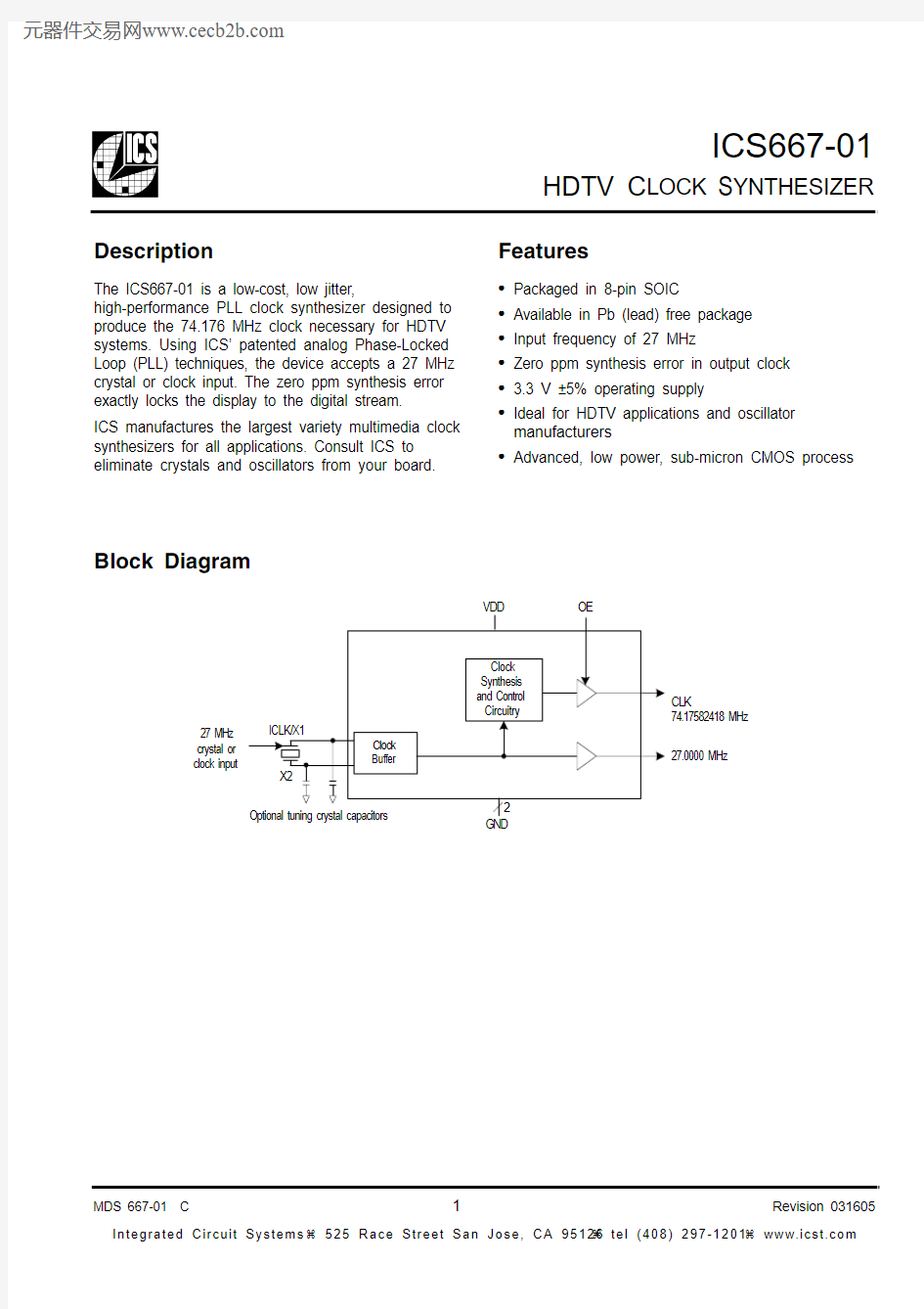
high-performance PLL clock synthesizer designed to produce the 74.176 MHz clock necessary for HDTV systems. Using ICS’ patented analog Phase-Locked Loop (PLL) techniques, the device accepts a 27 MHz crystal or clock input. The zero ppm synthesis error exactly locks the display to the digital stream.
ICS manufactures the largest variety multimedia clock synthesizers for all applications. Consult ICS to eliminate crystals and oscillators from your board.Features
?Packaged in 8-pin SOIC
?Available in Pb (lead) free package
?Input frequency of 27 MHz
?Zero ppm synthesis error in output clock
? 3.3 V ±5% operating supply
?Ideal for HDTV applications and oscillator manufacturers
?Advanced, low power, sub-micron CMOS process
Block Diagram
HDTV C LOCK S YNTHESIZER
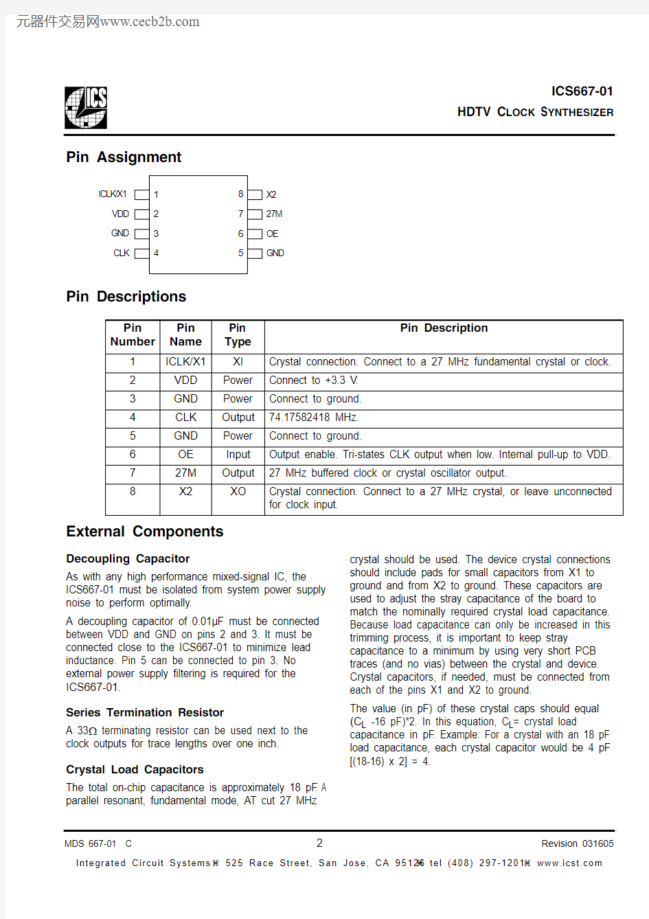
Pin Assignment
Pin Descriptions
External Components
Decoupling Capacitor
As with any high performance mixed-signal IC, the ICS667-01 must be isolated from system power supply noise to perform optimally.
A decoupling capacitor of 0.01μF must be connected between VDD and GND on pins 2 and 3. It must be connected close to the ICS667-01 to minimize lead inductance. Pin 5 can be connected to pin 3. No external power supply filtering is required for the ICS667-01.
Series Termination Resistor
A 33? terminating resistor can be used next to the clock outputs for trace lengths over one inch.
Crystal Load Capacitors
The total on-chip capacitance is approximately 18 pF . A parallel resonant, fundamental mode, AT cut 27 MHz
crystal should be used. The device crystal connections should include pads for small capacitors from X1 to ground and from X2 to ground. These capacitors are used to adjust the stray capacitance of the board to match the nominally required crystal load capacitance. Because load capacitance can only be increased in this trimming process, it is important to keep stray
capacitance to a minimum by using very short PCB traces (and no vias) between the crystal and device. Crystal capacitors, if needed, must be connected from each of the pins X1 and X2 to ground.
The value (in pF) of these crystal caps should equal (C L -16 pF)*2. In this equation, C L = crystal load
capacitance in pF . Example: For a crystal with an 18 pF load capacitance, each crystal capacitor would be 4 pF
[(18-16) x 2] = 4.
Pin Number
Pin Name
Pin Type
Pin Description
1ICLK/X1XI Crystal connection. Connect to a 27 MHz fundamental crystal or clock.
2VDD Power Connect to +3.3 V .3GND Power Connect to ground.4CLK Output 74.17582418 MHz. 5GND Power Connect to ground.
6OE Input Output enable. Tri-states CLK output when low. Internal pull-up to VDD.727M Output 27 MHz buffered clock or crystal oscillator output.
8
X2
XO
Crystal connection. Connect to a 27 MHz crystal, or leave unconnected for clock input.
HDTV C LOCK S YNTHESIZER
Absolute Maximum Ratings
Stresses above the ratings listed below can cause permanent damage to the ICS667-01. These ratings, which are standard values for ICS commercially rated parts, are stress ratings only. Functional operation of the device at these or any other conditions above those indicated in the operational sections of the
specifications is not implied. Exposure to absolute maximum rating conditions for extended periods can affect product reliability. Electrical parameters are guaranteed only over the recommended operating temperature range.
Recommended Operation Conditions
DC Electrical Characteristics
VDD=3.3 V+ 5% unless otherwise noted, Ambient temperature 0 to +70°C
Item
Rating
Supply Voltage, VDD 7 V
All Inputs and Outputs
-0.5 V to VDD+0.5 V Ambient Operating Temperature 0 to +70°C Storage Temperature -65 to +150°C Soldering Temperature
260°C
Parameter
Min.
Typ.
Max.
Units
Ambient Operating Temperature
0+70°C Power Supply Voltage (measured in respect to GND)
+3.150
3.3
+3.465
V
Parameter
Symbol
Conditions
Min.
Typ.
Max.
Units
Operating Voltage VDD 3.15 3.3
3.465V Input High Voltage V IH ICLK, OE 2.0
V Input Low Voltage V IL ICLK, OE 0.8
V Output High Voltage V OH I OH = -4 mA VDD-0.4
V Output Low Voltage V OL I OL = 4 mA 0.4
V Operating Supply Current IDD No load 30mA Short Circuit Current Each output
+50mA Input Capacitance
C IN
7
pF
HDTV C LOCK S YNTHESIZER
AC Electrical Characteristics
VDD =3.3V+ 5%, C L =15pF unless otherwise noted, Ambient Temperature 0 to +70°C
Thermal Characteristics
Marking Diagram
Marking Diagram (Pb free)
Notes:
1. ###### is the lot number.
2. YYWW is the last two digits of the year and week that the part was assembled.
3. Bottom marking: (origin)
Origin = country of origin if other than USA.4. “LF” denotes Pb (lead) free package.
Parameter
Symbol
Conditions Min.Typ.
Max.Units
Input Frequency
F IN 27
MHz Frequency Error, Output Clock 0
ppm Output Clock Rise Time t OR 0.8 to 2.0 V 1.5ns Output Clock Fall Time t
OF 2.0 to 8.0 V 1.5
ns Output Clock Duty Cycle
at 1.4 V
40
5060
%Maximum Absolute Jitter, short term t ja Deviation from mean 200ps Maximum Absolute Jitter, Long term term over 1us t jl
Deviation from mean 500ps Output Enable Time OE going from Low to High
20ns Internal Pull-up Resistor
R PUP
OE pin
750
k ?
Parameter
Symbol
Conditions
Min.Typ.
Max.Units
Thermal Resistance Junction to Ambient
θJA Still air 150°C/W θJA 1 m/s air flow 140°C/W θJA 3 m/s air flow
120°C/W Thermal Resistance Junction to Case
θJC
40
°C/W
HDTV C LOCK S YNTHESIZER
Package Outline and Package Dimensions (8-pin SOIC, 150 Mil. Narrow Body)
Package dimensions are kept current with JEDEC Publication No. 95
Ordering Information
Parts that are ordered with a "LF" suffix to the part number are the Pb-Free configuration and are RoHS compliant.While the information presented herein has been checked for both accuracy and reliability, Integrated Circuit Systems (ICS) assumes no responsibility for either its use or for the infringement of any patents or other rights of third parties, which would result from its use. No other circuits, patents, or licenses are implied. This product is intended for use in normal commercial applications. Any other applications such as those requiring extended temperature range, high reliability, or other extraordinary environmental requirements are not recommended without additional processing by ICS. ICS reserves the right to change any circuitry or specifications without notice. ICS does not authorize or warrant any ICS product for use in life support devices or critical medical instruments.
Part / Order Number
Marking
Shipping Packaging
Package
Temperature
ICS667M-01see page 5Tubes 8-pin SOIC 0 to +70° C ICS667M-01T Tape and Reel
8-pin SOIC 0 to +70° C ICS667M-01LF see page 5
Tubes 8-pin SOIC 0 to +70° C ICS667M-01LFT
Tape and Reel
8-pin SOIC
0 to +70° C