
(S )
https://www.doczj.com/doc/3913073816.html, 1
Data Sheet No. PD60162 Rev. V
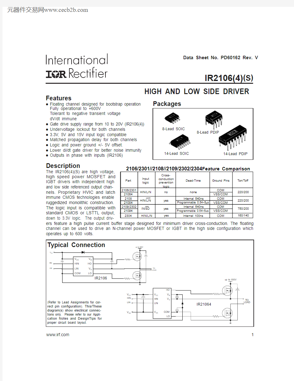
ers feature a high pulse current buffer stage designed for minimum driver cross-conduction. The floating channel can be used to drive an N-channel power MOSFET or IGBT in the high side configuration which operates up to 600 volts.
IR2106(4) (S
)
Absolute Maximum Ratings
Absolute maximum ratings indicate sustained limits beyond which damage to the device may occur. All voltage param-eters are absolute voltages referenced to COM. The thermal resistance and power dissipation ratings are measured
IR2106(4) (S
)
Note 1: Logic operational for V S of -5 to +600V. Logic state held for V S of -5V to -V BS . (Please refer to the Design Tip DT97-3 for more details).
Recommended Operating Conditions
The Input/Output logic timing diagram is shown in figure 1. For proper operation the device should be used within the recommended conditions. The V and V offset rating are tested with all supplies biased at 15V differential.
IR2106(4) (S
)
IR2106(4) (S
)
Functional Block Diagrams
IR2106(4) (S
)
14 Lead PDIP 14 Lead SOIC
IR21064IR21064S
Lead Assignments
8 Lead PDIP 8 Lead SOIC
Lead Definitions
Symbol Description
HIN Logic input for high side gate driver output (HO), in phase LIN Logic input for low side gate driver output (LO), in phase VSS Logic Ground (IR21064 only)V B High side floating supply HO High side gate drive output V S High side floating supply return V CC Low side and logic fixed supply LO Low side gate drive output COM
Low side return
IR2106IR2106S
1234
8
765
V CC HIN LIN COM
V B HO V S LO
1234
8
765
V CC HIN LIN COM
V B HO V S LO
1234567
14
1312111098
V CC HIN LIN
VSS COM LO
V B HO V S
1234567
14
1312111098
V CC HIN LIN
VSS COM LO
V B HO V S
IR2106(4) (S
)
Figure 1. Input/Output Timing Diagram
HIN LIN
HO LO
Figure 2. Switching Time Waveform Definitions
IR2106(4) (S
)
IR2106(4) (S
)
IR2106(4) (S
)
IR2106(4) (S
)
IR2106(4) (S
)
(A (A (A 300
(A
IR2106(4) (S
)
(A (A (A (A
IR2106(4) (S
)
(A (A
IR2106(4) (S
)
(A (A
IR2106(4) (S
)
( A
( A
IR2106(4) (S
)
IR2106(4) (S
)
IR2106(4) (S
)
IR2106(4) (S
)