Winbond
Bus Termination Regulator
W83310S-R2
W83310G-R2
Publication Release Date: January 17, 2005
-I-
Revision 0.53
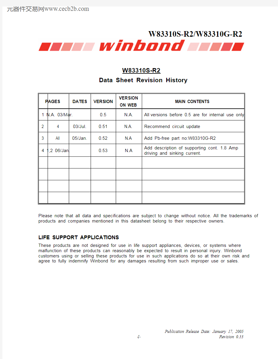
W83310S-R2
Data Sheet Revision History
PAGES DATES VERSION
VERSION
ON WEB
MAIN CONTENTS
1 N.A. 03/Mar. 0.5 N.A. All versions before 0.5 are for internal use only
2 4 03/Jul. 0.51 N.A. Recommend circuit update 3
All
05/Jan.
0.52
N.A Add Pb-free part no:W83310G-R2
4 1,2 06/Jan. 0.53 N.A Add description of supporting cont. 1.8 Amp
driving and sinking current.
Please note that all data and specifications are subject to change without notice. All the trademarks of products and companies mentioned in this datasheet belong to their respective owners.
LIFE SUPPORT APPLICATIONS
These products are not designed for use in life support appliances, devices, or systems where malfunction of these products can reasonably be expected to result in personal injury. Winbond customers using or selling these products for use in such applications do so at their own risk and agree to fully indemnify Winbond for any damages resulting from such improper use or sales.
Table of Contents-
1.GENERAL DESCRIPTION (1)
2.FEATURES (1)
3.APPLICATIONS (1)
4.PIN CONFIGURATION AND DESCRIPTION (2)
5.APPLICATION CIRCUIT (3)
6.INTERNAL BLOCK DIAGRAM (4)
7.ELECTRICAL CHARACTERISTICS (5)
7.1AC CHARACTERISTICS (5)
8.TYPICAL OPERATING WAVEFORM (6)
9.PACKAGE DIMENSION (8)
10.ORDERING INFORMATION (9)
11.HOW TO READ THE TOP MARKING (9)
-II-
Publication Release Date: January 17, 2005
-1-
Revision 0.53
1. GENERAL DESCRIPTION
The W83310S-R2 is a linear regulator which provides achieves peak 2.0 Amp/cont. 1.8 Amp bi-directional sinking and driving capability for DDR SDRAM bus terminator application. The chip simply implement a stable power supply which can track half of input power dynamically for bus terminator with a single chip; that is the chip integrates two power MOSFETs. There is no any external power device needed. The W83310S-R2 is promoted with small footprint 8-SOP 150mil package. With W83301S-R2 design, a high integration, high performance, and cost-effective solution is promoted.
2. FEATURES
y Regulates a bi-directional power with driving and sinking capability y Provides achieve peak 2.0 Amp/cont. 1.8 Amp driving and sinking current y Power MOSFET integrated y Low external component count y Low output voltage offset
y Operates with +3.3V and +2.5V control power y Small package
y
Low cost and easy to use
3. APPLICATIONS
y DDR Bus Termination Regulator y
Active Termination Bus
y SSTL-2 y SSTL-3
W83310S-R2/W83310G-R2
-2-
4. PIN CONFIGURATION AND DESCRIPTION
- W83310S-R2
SYMBOL
PIN
FUNCTION
VIN 1 Power input pin.
GND 2 Ground. VREF
3
Reference voltage and Chip enable.
VOUT 4 Output voltage. VCNTL 5 Gate drive voltage. VCNTL 6 Gate drive voltage. VCNTL 7 Gate drive voltage. VCNTL 8 Gate drive voltage.
I inbond
W83310S-R2
5. APPLICATION CIRCUIT
Publication Release Date: January 17, 2005
-3- Revision 0.53
6. INTERNAL BLOCK DIAGRAM
-4-
Publication Release Date: January 17, 2005
-5-
Revision 0.53
7. ELECTRICAL CHARACTERISTICS
7.1 AC CHARACTERISTICS
W83310S-R2
VIN=2.5V,VCNTL=3.3V,VREF=1.25V,Cout=100uF, T A = 0°C to +70°C
PARAMETER
SYMBOL
MIN
TYP
MAX
UNITS
TEST
CONDITIONS
Output Offset Voltage V OS
-5 0 +5 mV I OUT =0A 1.0 Loading: 0A ?2.0A Load Regulation
1.0 %
Loading: 0A ?-2.0A V IN 2.5 3.63Input Voltage Range V CNTL 3.3 3.63
V
Operating Current of
VCNTL I CNTL
0.5 1.0 mA No Load(I OUT =0A)0.8 V Output =
High Shutdown Threshold
Trigger 0.2 V Output =
Low Shutdown Current I SHDN 10 uA
VREF<0.2V Loading=0.7A Short Current Limit I LMT
4.0 A
Note : Load regulation is tested with a 1ms duty pulse current and measuring V OUT .
-6-
8. TYPICAL OPERATING WAVEFORM
Load regulation with test condition - V CTRL =3.3V; V IN =2.5V; V OUT =1.25V; 2.0Amp 1ms duty pulse
driving current. ΔV ≈ 9mV.
Load regulation with test condition - V CTRL
=3.3V; V IN =2.5V; V OUT =1.25V; 2.0Amp 1ms duty pulse sinking current. ΔV ≈ 4mV.
Publication Release Date: January 17, 2005
-7-
Revision 0.53
Load regulation with test condition - V CTRL =3.3V; V IN =2.5V; V OUT =1.25V; 1.8Amp cont. driving current. ΔV ≈ 32mV @ ~85℃
.
Load regulation with test condition - V CTRL =3.3V; V IN =2.5V; V OUT =1.25V; 1.8Amp cont. sinking current. ΔV ≈ 2mV @ ~85℃
.
9. PACKAGE DIMENSION
8L SOP 150mil
-8-
Publication Release Date: January 17, 2005
-9-
Revision 0.53
10. ORDERING INFORMATION
PART NUMBER
PACKAGE TYPE
PRODUCTION FLOW
W83310S-R2 8 PIN SOP
Commercial, 0°C to +70°C W83310G-R2
8 PIN SOP(Pb-free package)
Commercial, 0°C to +70°C
11. HOW TO READ THE TOP MARKING
W83 310G-R2249OB
W83 310S-R2 249OB
Left line: Winbond logo
1st & 2nd line: W83310S-R2 – the part number , W83310G-R2-the Pb-free part number 3rd line: Tracking code Tracking code 249 O A 249: packages assembled in Year 02’, week 49
O : assembly house ID; O means OSE, G means GR, etc. B : the IC version
-10-
Important Notice
Winbond products are not designed, intended, authorized or warranted for use as components in systems or equipment intended for surgical implantation, atomic energy control instruments, airplane or spaceship instruments, transportation instruments, traffic signal instruments, combustion control instruments, or for other applications intended to support or sustain life. Further more, Winbond products are not intended for applications wherein failure of Winbond products could result or lead to a situation wherein personal injury, death or severe property or environmental damage could occur.
Winbond customers using or selling these products for use in such applications do so at their own risk and agree to fully indemnify Winbond for any damages resulting from such improper use or sales.