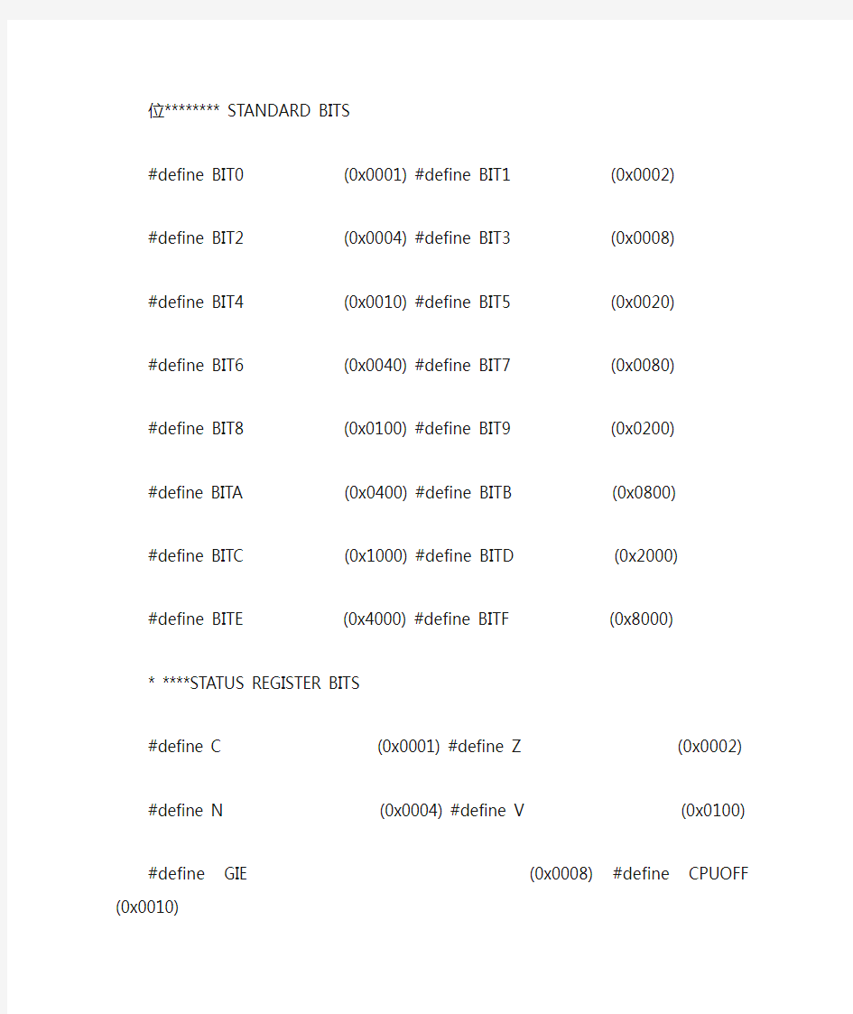
位******** STANDARD BITS
#define BIT0 (0x0001) #define BIT1 (0x0002)
#define BIT2 (0x0004) #define BIT3 (0x0008)
#define BIT4 (0x0010) #define BIT5 (0x0020)
#define BIT6 (0x0040) #define BIT7 (0x0080)
#define BIT8 (0x0100) #define BIT9 (0x0200)
#define BITA (0x0400) #define BITB (0x0800)
#define BITC (0x1000) #define BITD (0x2000)
#define BITE (0x4000) #define BITF (0x8000)
* ****STATUS REGISTER BITS
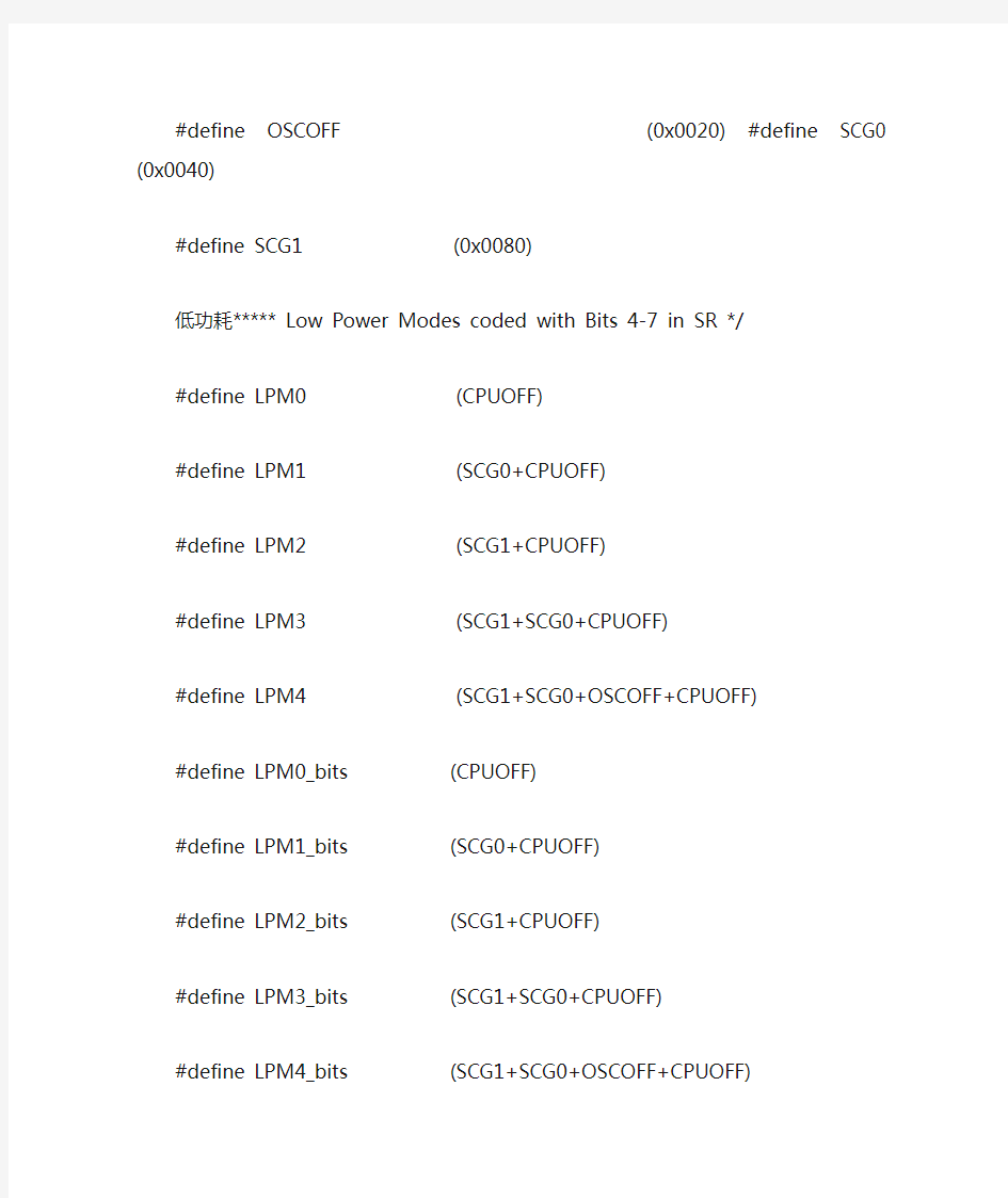
#define C (0x0001) #define Z (0x0002) #define N (0x0004) #define V (0x0100) #define GIE (0x0008) #define CPUOFF (0x0010) #define OSCOFF (0x0020) #define SCG0 (0x0040) #define SCG1 (0x0080)
低功耗***** Low Power Modes coded with Bits 4-7 in SR */
#define LPM0 (CPUOFF)
#define LPM1 (SCG0+CPUOFF)
#define LPM2 (SCG1+CPUOFF)
#define LPM3 (SCG1+SCG0+CPUOFF)
#define LPM4 (SCG1+SCG0+OSCOFF+CPUOFF)
#define LPM0_bits (CPUOFF)
#define LPM1_bits (SCG0+CPUOFF)
#define LPM2_bits (SCG1+CPUOFF)
#define LPM3_bits (SCG1+SCG0+CPUOFF)
#define LPM4_bits (SCG1+SCG0+OSCOFF+CPUOFF)
**********#include
#define LPM0 _BIS_SR(LPM0_bits) /* Enter Low Power Mode 0 */
#define LPM0_EXIT _BIC_SR_IRQ(LPM0_bits) /* Exit Low Power Mode 0 */
#define LPM1 _BIS_SR(LPM1_bits) /* Enter Low Power Mode 1 */
#define LPM1_EXIT _BIC_SR_IRQ(LPM1_bits) /* Exit Low Power Mode 1 */
#define LPM2 _BIS_SR(LPM2_bits) /* Enter Low Power Mode 2 */
#define LPM2_EXIT _BIC_SR_IRQ(LPM2_bits) /* Exit Low Power Mode 2 */
#define LPM3 _BIS_SR(LPM3_bits) /* Enter Low Power Mode 3 */
#define LPM3_EXIT _BIC_SR_IRQ(LPM3_bits) /* Exit Low Power Mode 3 */
#define LPM4 _BIS_SR(LPM4_bits) /* Enter Low Power Mode 4 */
#define LPM4_EXIT _BIC_SR_IRQ(LPM4_bits) /* Exit Low Power Mode 4 */
使能*********** PERIPHERAL FILE MAP
#define IE1_ (0x0000) /* Interrupt Enable 1 */
DEFC( IE1 , IE1_)
#define U0IE IE1 /* UART0 Interrupt Enable Register */
#define WDTIE (0x01) #define OFIE (0x02)
#define NMIIE (0x10) #define ACCVIE (0x20)
#define URXIE0 (0x40) #define UTXIE0 (0x80)
#define IFG1_ (0x0002) /* Interrupt Flag 1 */
DEFC( IFG1 , IFG1_)
#define U0IFG IFG1 /* UART0 Interrupt Flag Register */
#define WDTIFG (0x01) #define OFIFG (0x02)
#define NMIIFG (0x10) #define URXIFG0 (0x40)
#define UTXIFG0 (0x80)
#define ME1_ (0x0004) /* Module Enable 1 */
DEFC( ME1 , ME1_)
#define U0ME ME1 /* UART0 Module Enable Register */
#define URXE0 (0x40) #define UTXE0 (0x80)
#define USPIE0 (0x40)
#define IE2_ (0x0001) /* Interrupt Enable 2 */
DEFC( IE2 , IE2_)
#define U1IE IE2 /* UART1 Interrupt Enable Register */
#define URXIE1 (0x10) #define UTXIE1 (0x20)
#define IFG2_ (0x0003) /* Interrupt Flag 2 */
DEFC( IFG2 , IFG2_)
#define U1IFG IFG2 /* UART1 Interrupt Flag Register */
#define URXIFG1 (0x10) #define UTXIFG1 (0x20)
#define ME2_ (0x0005) /* Module Enable 2 */
DEFC( ME2 , ME2_)
#define U1ME ME2 /* UART1 Module Enable Register */
#define URXE1 (0x10)
#define UTXE1 (0x20)
#define USPIE1 (0x10)
看门狗************* WATCHDOG TIMER
#define WDTCTL_ (0x0120) /* Watchdog Timer Control */
DEFW( WDTCTL , WDTCTL_)
/* The bit names have been prefixed with "WDT" */
#define WDTIS0 (0x0001)
#define WDTIS1 (0x0002)
#define WDTSSEL (0x0004)
#define WDTCNTCL (0x0008)
#define WDTTMSEL (0x0010)
#define WDTNMI (0x0020)
#define WDTNMIES (0x0040)
#define WDTHOLD (0x0080)
#define WDTPW (0x5A00)
/* WDT is clocked by fSMCLK (assumed 1MHz) */
#define WDT_MDL Y_32 /* 32ms (WDTPW+WDTTMSEL+WDTCNTCL) #define WDT_MDL Y_8 /* 8ms (WDTPW+WDTTMSEL+WDTCNTCL+WDTIS0) #define WDT_MDL Y_0_5 /* 0.5ms (WDTPW+WDTTMSEL+WDTCNTCL+WDTIS1) #define WDT_MDL Y_0_064 (WDTPW+WDTTMSEL+WDTCNTCL+WDTIS1+WDTIS0) /* 0.064ms " */
/* WDT is clocked by fACLK (assumed 32KHz) */
#define WDT_ADL Y_1000 /* (WDTPW+WDTTMSEL+WDTCNTCL+WDTSSEL) " *//* 1000ms
#define WDT_ADL Y_250 (WDTPW+WDTTMSEL+WDTCNTCL+WDTSSEL+WDTIS0) /* 250ms " */
#define WDT_ADL Y_16 (WDTPW+WDTTMSEL+WDTCNTCL+WDTSSEL+WDTIS1) /* 16ms " */
#define WDT_ADL Y_1_9 (WDTPW+WDTTMSEL+WDTCNTCL+WDTSSEL+WDTIS1+WDTIS0) /* 1.9ms " */
/* Watchdog mode -> reset after expired time */
/* WDT is clocked by fSMCLK (assumed 1MHz) */
#define WDT_MRST_32 (WDTPW+WDTCNTCL) /* 32ms interval (default) */
#define WDT_MRST_8 8ms (WDTPW+WDTCNTCL+WDTIS0)
#define WDT_MRST_0_5 0.5ms (WDTPW+WDTCNTCL+WDTIS1)
#define WDT_MRST_0_064 0.064ms (WDTPW+WDTCNTCL+WDTIS1+WDTIS0)
/* WDT is clocked by fACLK (assumed 32KHz) */
#define WDT_ARST_1000 1000ms (WDTPW+WDTCNTCL+WDTSSEL)
#define WDT_ARST_250 250ms (WDTPW+WDTCNTCL+WDTSSEL+WDTIS0)
#define WDT_ARST_16 16ms (WDTPW+WDTCNTCL+WDTSSEL+WDTIS1)
#define WDT_ARST_1_9 (WDTPW+WDTCNTCL+WDTSSEL+WDTIS1+WDTIS0) /* 1.9ms " */ /* INTERRUPT CONTROL *************
/* These two bits are defined in the Special Function Registers */
/* #define WDTIE 0x01 *//* #define WDTIFG 0x01 */
********* HARDW ARE MULTIPLIER
#define MPY_ (0x0130) /* Multiply Unsigned/Operand 1 */
DEFW( MPY , MPY_)
#define MPYS_ (0x0132) /* Multiply Signed/Operand 1 */
DEFW( MPYS , MPYS_)
#define MAC_ (0x0134) /* Multiply Unsigned and Accumulate/Operand 1 */ DEFW( MAC , MAC_)
#define MACS_ (0x0136) /* Multiply Signed and Accumulate/Operand 1 */ DEFW( MACS , MACS_)
#define OP2_ (0x0138) /* Operand 2 */
DEFW( OP2 , OP2_)
#define RESLO_ (0x013A) /* Result Low Word */
DEFW( RESLO , RESLO_)
#define RESHI_ (0x013C) /* Result High Word */
DEFW( RESHI , RESHI_)
#define SUMEXT_ (0x013E) /* Sum Extend */
READ_ONL Y DEFW( SUMEXT , SUMEXT_)
引脚1、2********** DIGITAL I/O Port1/2
#define P1IN_ (0x0020) /* Port 1 Input */
READ_ONL Y DEFC( P1IN , P1IN_)
#define P1OUT_ (0x0021) /* Port 1 Output */
DEFC( P1OUT , P1OUT_)
#define P1DIR_ (0x0022) /* Port 1 Direction */
DEFC( P1DIR , P1DIR_)
#define P1IFG_ (0x0023) /* Port 1 Interrupt Flag */
DEFC( P1IFG , P1IFG_)
#define P1IES_ (0x0024) /* Port 1 Interrupt Edge Select */
DEFC( P1IES , P1IES_)
#define P1IE_ (0x0025) /* Port 1 Interrupt Enable */
DEFC( P1IE , P1IE_)
#define P1SEL_ (0x0026) /* Port 1 Selection */
DEFC( P1SEL , P1SEL_)
#define P2IN_ (0x0028) /* Port 2 Input */
READ_ONL Y DEFC( P2IN , P2IN_)
#define P2OUT_ (0x0029) /* Port 2 Output */
DEFC( P2OUT , P2OUT_)
#define P2DIR_ (0x002A) /* Port 2 Direction */
DEFC( P2DIR , P2DIR_)
#define P2IFG_ (0x002B) /* Port 2 Interrupt Flag */
DEFC( P2IFG , P2IFG_)
#define P2IES_ (0x002C) /* Port 2 Interrupt Edge Select */
DEFC( P2IES , P2IES_)
#define P2IE_ (0x002D) /* Port 2 Interrupt Enable */
DEFC( P2IE , P2IE_)
#define P2SEL_ (0x002E) /* Port 2 Selection */
DEFC( P2SEL , P2SEL_)
引脚3,4*********** DIGITAL I/O Port3/4
#define __MSP430_HAS_PORT3__ /* Definition to show that Module is available */ #define __MSP430_HAS_PORT4__ /* Definition to show that Module is available */ #define P3IN_ (0x0018) /* Port 3 Input */
READ_ONL Y DEFC( P3IN , P3IN_)
#define P3OUT_ (0x0019) /* Port 3 Output */
DEFC( P3OUT , P3OUT_)
#define P3DIR_ (0x001A) /* Port 3 Direction */
DEFC( P3DIR , P3DIR_)
#define P3SEL_ (0x001B) /* Port 3 Selection */
DEFC( P3SEL , P3SEL_)
#define P4IN_ (0x001C) /* Port 4 Input */
READ_ONL Y DEFC( P4IN , P4IN_)
#define P4OUT_ (0x001D) /* Port 4 Output */
DEFC( P4OUT , P4OUT_)
#define P4DIR_ (0x001E) /* Port 4 Direction */
DEFC( P4DIR , P4DIR_)
#define P4SEL_ (0x001F) /* Port 4 Selection */
DEFC( P4SEL , P4SEL_)
引脚5.6*********** DIGITAL I/O Port5/6
#define P5IN_ (0x0030) /* Port 5 Input */
READ_ONL Y DEFC( P5IN , P5IN_)
#define P5OUT_ (0x0031) /* Port 5 Output */
DEFC( P5OUT , P5OUT_)
#define P5DIR_ (0x0032) /* Port 5 Direction */
DEFC( P5DIR , P5DIR_)
#define P5SEL_ (0x0033) /* Port 5 Selection */
DEFC( P5SEL , P5SEL_)
#define P6IN_ (0x0034) /* Port 6 Input */
READ_ONL Y DEFC( P6IN , P6IN_)
#define P6OUT_ (0x0035) /* Port 6 Output */
DEFC( P6OUT , P6OUT_)
#define P6DIR_ (0x0036) /* Port 6 Direction */
DEFC( P6DIR , P6DIR_)
#define P6SEL_ (0x0037) /* Port 6 Selection */
DEFC( P6SEL , P6SEL_)
串口*************** USART
/* UxCTL */
#define PENA (0x80) /* Parity enable */
#define PEV (0x40) /* Parity 0:odd / 1:even */
#define SPB (0x20) /* Stop Bits 0:one / 1: two */
#define CHAR (0x10) /* Data 0:7-bits / 1:8-bits */
#define LISTEN (0x08) /* Listen mode */
#define SYNC (0x04) /* UART / SPI mode */
#define MM (0x02) /* Master Mode off/on */
#define SWRST (0x01) /* USART Software Reset */
/* UxTCTL */
#define CKPH (0x80) /* SPI: Clock Phase */
#define CKPL (0x40) /* Clock Polarity */
#define SSEL1 (0x20) /* Clock Source Select 1 */
#define SSEL0 (0x10) /* Clock Source Select 0 */
#define URXSE (0x08) /* Receive Start edge select */
#define TXW AKE (0x04) /* TX Wake up mode */
#define STC (0x02) /* SPI: STC enable 0:on / 1:off */ #define TXEPT (0x01) /* TX Buffer empty */
/* UxRCTL */
#define FE (0x80) /* Frame Error */
#define PE (0x40) /* Parity Error */
#define OE (0x20) /* Overrun Error */
#define BRK (0x10) /* Break detected */
#define URXEIE (0x08) /* RX Error interrupt enable */
#define URXWIE (0x04) /* RX Wake up interrupt enable */
#define RXW AKE (0x02) /* RX Wake up detect */
#define RXERR (0x01) /* RX Error Error */
串口0***************** USART 0
#define U0CTL_ (0x0070) /* USART 0 Control */
DEFC( U0CTL , U0CTL_)
#define U0TCTL_ (0x0071) /* USART 0 Transmit Control */ DEFC( U0TCTL , U0TCTL_)
#define U0RCTL_ (0x0072) /* USART 0 Receive Control */ DEFC( U0RCTL , U0RCTL_)
#define U0MCTL_ (0x0073) /* USART 0 Modulation Control */ DEFC( U0MCTL , U0MCTL_)
#define U0BR0_ (0x0074) /* USART 0 Baud Rate 0 */
DEFC( U0BR0 , U0BR0_)
#define U0BR1_ (0x0075) /* USART 0 Baud Rate 1 */
DEFC( U0BR1 , U0BR1_)
#define U0RXBUF_ (0x0076) /* USART 0 Receive Buffer */ READ_ONL Y DEFC( U0RXBUF , U0RXBUF_)
#define U0TXBUF_ (0x0077) /* USART 0 Transmit Buffer */ DEFC( U0TXBUF , U0TXBUF_)
#define UCTL0 U0CTL /* USART 0 Control */
#define UTCTL0 U0TCTL /* USART 0 Transmit Control */
#define URCTL0 U0RCTL /* USART 0 Receive Control */
#define UMCTL0 U0MCTL /* USART 0 Modulation Control */ #define UBR00 U0BR0 /* USART 0 Baud Rate 0 */
#define UBR10 U0BR1 /* USART 0 Baud Rate 1 */
#define RXBUF0 U0RXBUF /* USART 0 Receive Buffer */
#define TXBUF0 U0TXBUF /* USART 0 Transmit Buffer */
#define UCTL0_ U0CTL_ /* USART 0 Control */
#define UTCTL0_ U0TCTL_ /* USART 0 Transmit Control */
#define URCTL0_ U0RCTL_ /* USART 0 Receive Control */
#define UMCTL0_ U0MCTL_ /* USART 0 Modulation Control */ #define UBR00_ U0BR0_ /* USART 0 Baud Rate 0 */
#define UBR10_ U0BR1_ /* USART 0 Baud Rate 1 */
#define RXBUF0_ U0RXBUF_ /* USART 0 Receive Buffer */
#define TXBUF0_ U0TXBUF_ /* USART 0 Transmit Buffer */
#define UCTL_0 U0CTL /* USART 0 Control */
#define UTCTL_0 U0TCTL /* USART 0 Transmit Control */
#define URCTL_0 U0RCTL /* USART 0 Receive Control */
#define UMCTL_0 U0MCTL /* USART 0 Modulation Control */ #define UBR0_0 U0BR0 /* USART 0 Baud Rate 0 */
#define UBR1_0 U0BR1 /* USART 0 Baud Rate 1 */
#define RXBUF_0 U0RXBUF /* USART 0 Receive Buffer */
#define TXBUF_0 U0TXBUF /* USART 0 Transmit Buffer */
#define UCTL_0_ U0CTL_ /* USART 0 Control */
#define UTCTL_0_ U0TCTL_ /* USART 0 Transmit Control */
#define URCTL_0_ U0RCTL_ /* USART 0 Receive Control */
#define UMCTL_0_ U0MCTL_ /* USART 0 Modulation Control */ #define UBR0_0_ U0BR0_ /* USART 0 Baud Rate 0 */
#define UBR1_0_ U0BR1_ /* USART 0 Baud Rate 1 */
#define RXBUF_0_ U0RXBUF_ /* USART 0 Receive Buffer */
#define TXBUF_0_ U0TXBUF_ /* USART 0 Transmit Buffer */
串口1**USART 1 *******
#define U1CTL_ (0x0078) /* USART 1 Control */
DEFC( U1CTL , U1CTL_)
#define U1TCTL_ (0x0079) /* USART 1 Transmit Control */ DEFC( U1TCTL , U1TCTL_)
#define U1RCTL_ (0x007A) /* USART 1 Receive Control */ DEFC( U1RCTL , U1RCTL_)
#define U1MCTL_ (0x007B) /* USART 1 Modulation Control */ DEFC( U1MCTL , U1MCTL_)
#define U1BR0_ (0x007C) /* USART 1 Baud Rate 0 */
DEFC( U1BR0 , U1BR0_)
#define U1BR1_ (0x007D) /* USART 1 Baud Rate 1 */
DEFC( U1BR1 , U1BR1_)
#define U1RXBUF_ (0x007E) /* USART 1 Receive Buffer */ READ_ONL Y DEFC( U1RXBUF , U1RXBUF_)
#define U1TXBUF_ (0x007F) /* USART 1 Transmit Buffer */ DEFC( U1TXBUF , U1TXBUF_)
#define UCTL1 U1CTL /* USART 1 Control */
#define UTCTL1 U1TCTL /* USART 1 Transmit Control */
#define URCTL1 U1RCTL /* USART 1 Receive Control */
#define UMCTL1 U1MCTL /* USART 1 Modulation Control */ #define UBR01 U1BR0 /* USART 1 Baud Rate 0 */
#define UBR11 U1BR1 /* USART 1 Baud Rate 1 */
#define RXBUF1 U1RXBUF /* USART 1 Receive Buffer */
#define TXBUF1 U1TXBUF /* USART 1 Transmit Buffer */
#define UCTL1_ U1CTL_ /* USART 1 Control */
#define UTCTL1_ U1TCTL_ /* USART 1 Transmit Control */
#define URCTL1_ U1RCTL_ /* USART 1 Receive Control */
#define UMCTL1_ U1MCTL_ /* USART 1 Modulation Control */ #define UBR01_ U1BR0_ /* USART 1 Baud Rate 0 */
#define UBR11_ U1BR1_ /* USART 1 Baud Rate 1 */
#define RXBUF1_ U1RXBUF_ /* USART 1 Receive Buffer */
#define TXBUF1_ U1TXBUF_ /* USART 1 Transmit Buffer */
#define UCTL_1 U1CTL /* USART 1 Control */
#define UTCTL_1 U1TCTL /* USART 1 Transmit Control */
#define URCTL_1 U1RCTL /* USART 1 Receive Control */
#define UMCTL_1 U1MCTL /* USART 1 Modulation Control */
#define UBR0_1 U1BR0 /* USART 1 Baud Rate 0 */
#define UBR1_1 U1BR1 /* USART 1 Baud Rate 1 */
#define RXBUF_1 U1RXBUF /* USART 1 Receive Buffer */
#define TXBUF_1 U1TXBUF /* USART 1 Transmit Buffer */
#define UCTL_1_ U1CTL_ /* USART 1 Control */
#define UTCTL_1_ U1TCTL_ /* USART 1 Transmit Control */
#define URCTL_1_ U1RCTL_ /* USART 1 Receive Control */
#define UMCTL_1_ U1MCTL_ /* USART 1 Modulation Control */
#define UBR0_1_ U1BR0_ /* USART 1 Baud Rate 0 */
#define UBR1_1_ U1BR1_ /* USART 1 Baud Rate 1 */
#define RXBUF_1_ U1RXBUF_ /* USART 1 Receive Buffer */
#define TXBUF_1_ U1TXBUF_ /* USART 1 Transmit Buffer */
定时器1* Timer A3**************************
#define __MSP430_HAS_TA3__ /* Definition to show that Module is available */ #define TAIV_ (0x012E) /* Timer A Interrupt Vector Word */
READ_ONL Y DEFW( TAIV , TAIV_)
#define TACTL_ (0x0160) /* Timer A Control */
DEFW( TACTL , TACTL_)
#define TACCTL0_ (0x0162) /* Timer A Capture/Compare Control 0 */ DEFW( TACCTL0 , TACCTL0_)
#define TACCTL1_ (0x0164) /* Timer A Capture/Compare Control 1 */ DEFW( TACCTL1 , TACCTL1_)
#define TACCTL2_ (0x0166) /* Timer A Capture/Compare Control 2 */ DEFW( TACCTL2 , TACCTL2_)
#define TAR_ (0x0170) /* Timer A */
DEFW( TAR , TAR_)
#define TACCR0_ (0x0172) /* Timer A Capture/Compare 0 */
DEFW( TACCR0 , TACCR0_)
#define TACCR1_ (0x0174) /* Timer A Capture/Compare 1 */
DEFW( TACCR1 , TACCR1_)
#define TACCR2_ (0x0176) /* Timer A Capture/Compare 2 */
DEFW( TACCR2 , TACCR2_)
#define CCTL0 TACCTL0 /* Timer A Capture/Compare Control 0 */
#define CCTL1 TACCTL1 /* Timer A Capture/Compare Control 1 */
#define CCTL2 TACCTL2 /* Timer A Capture/Compare Control 2 */
#define CCR0 TACCR0 /* Timer A Capture/Compare 0 */
#define CCR1 TACCR1 /* Timer A Capture/Compare 1 */
#define CCR2 TACCR2 /* Timer A Capture/Compare 2 */
#define CCTL0_ TACCTL0_ /* Timer A Capture/Compare Control 0 */
#define CCTL1_ TACCTL1_ /* Timer A Capture/Compare Control 1 */
#define CCTL2_ TACCTL2_ /* Timer A Capture/Compare Control 2 */
#define CCR0_ TACCR0_ /* Timer A Capture/Compare 0 */
#define CCR1_ TACCR1_ /* Timer A Capture/Compare 1 */
#define CCR2_ TACCR2_ /* Timer A Capture/Compare 2 */
#define TASSEL1 (0x0200) /* Timer A clock source select 0 */
#define TASSEL0 (0x0100) /* Timer A clock source select 1 */
#define ID1 (0x0080) /* Timer A clock input divider 1 */
#define ID0 (0x0040) /* Timer A clock input divider 0 */
#define MC1 (0x0020) /* Timer A mode control 1 */
#define MC0 (0x0010) /* Timer A mode control 0 */
#define TACLR (0x0004) /* Timer A counter clear */
#define TAIE (0x0002) /* Timer A counter interrupt enable */
#define TAIFG (0x0001) /* Timer A counter interrupt flag */
#define MC_0 (0*0x10u) /* Timer A mode control: 0 - Stop */
#define MC_1 (1*0x10u) /* Timer A mode control: 1 - Up to CCR0 */
#define MC_2 (2*0x10u) /* Timer A mode control: 2 - Continous up */
#define MC_3 (3*0x10u) /* Timer A mode control: 3 - Up/Down */
#define ID_0 (0*0x40u) /* Timer A input divider: 0 - /1 */
#define ID_1 (1*0x40u) /* Timer A input divider: 1 - /2 */
#define ID_2 (2*0x40u) /* Timer A input divider: 2 - /4 */
#define ID_3 (3*0x40u) /* Timer A input divider: 3 - /8 */
#define TASSEL_0 (0*0x100u) /* Timer A clock source select: 0 - TACLK */
#define TASSEL_1 (1*0x100u) /* Timer A clock source select: 1 - ACLK */
#define TASSEL_2 (2*0x100u) /* Timer A clock source select: 2 - SMCLK */
#define TASSEL_3 (3*0x100u) /* Timer A clock source select: 3 - INCLK */
#define CM1 (0x8000) /* Capture mode 1 */
#define CM0 (0x4000) /* Capture mode 0 */
#define CCIS1 (0x2000) /* Capture input select 1 */
#define CCIS0 (0x1000) /* Capture input select 0 */
#define SCS (0x0800) /* Capture sychronize */
#define SCCI (0x0400) /* Latched capture signal (read) */
#define CAP (0x0100) /* Capture mode: 1 /Compare mode : 0 */
#define OUTMOD2 (0x0080) /* Output mode 2 */
#define OUTMOD1 (0x0040) /* Output mode 1 */
#define OUTMOD0 (0x0020) /* Output mode 0 */
#define CCIE (0x0010) /* Capture/compare interrupt enable */
#define CCI (0x0008) /* Capture input signal (read) */
#define OUT (0x0004) /* PWM Output signal if output mode 0 */
#define COV (0x0002) /* Capture/compare overflow flag */
#define CCIFG (0x0001) /* Capture/compare interrupt flag */
#define OUTMOD_0 (0*0x20u) /* PWM output mode: 0 - output only */
#define OUTMOD_1 (1*0x20u) /* PWM output mode: 1 - set */
#define OUTMOD_2 (2*0x20u) /* PWM output mode: 2 - PWM toggle/reset */ #define OUTMOD_3 (3*0x20u) /* PWM output mode: 3 - PWM set/reset */
#define OUTMOD_4 (4*0x20u) /* PWM output mode: 4 - toggle */
#define OUTMOD_5 (5*0x20u) /* PWM output mode: 5 - Reset */
#define OUTMOD_6 (6*0x20u) /* PWM output mode: 6 - PWM toggle/set */ #define OUTMOD_7 (7*0x20u) /* PWM output mode: 7 - PWM reset/set */
#define CCIS_0 (0*0x1000u) /* Capture input select: 0 - CCIxA */
#define CCIS_1 (1*0x1000u) /* Capture input select: 1 - CCIxB */
#define CCIS_2 (2*0x1000u) /* Capture input select: 2 - GND */
#define CCIS_3 (3*0x1000u) /* Capture input select: 3 - Vcc */
#define CM_0 (0*0x4000u) /* Capture mode: 0 - disabled */
#define CM_1 (1*0x4000u) /* Capture mode: 1 - pos. edge */
#define CM_2 (2*0x4000u) /* Capture mode: 1 - neg. edge */
#define CM_3 (3*0x4000u) /* Capture mode: 1 - both edges */
#define TAIV_NONE (0x0000) /* No Interrupt pending */
#define TAIV_TACCR1 (0x0002) /* TACCR1_CCIFG */
#define TAIV_TACCR2 (0x0004) /* TACCR2_CCIFG */
#define TAIV_6 (0x0006) /* Reserved */
#define TAIV_8 (0x0008) /* Reserved */
#define TAIV_TAIFG (0x000A) /* TAIFG */
定时器2* Timer B7*********************************
#define TBIV_ (0x011E) /* Timer B Interrupt Vector Word */ READ_ONL Y DEFW( TBIV , TBIV_)
#define TBCTL_ (0x0180) /* Timer B Control */
DEFW( TBCTL , TBCTL_)
#define TBCCTL0_ (0x0182) /* Timer B Capture/Compare Control 0 */ DEFW( TBCCTL0 , TBCCTL0_)
#define TBCCTL1_ (0x0184) /* Timer B Capture/Compare Control 1 */ DEFW( TBCCTL1 , TBCCTL1_)
#define TBCCTL2_ (0x0186) /* Timer B Capture/Compare Control 2 */ DEFW( TBCCTL2 , TBCCTL2_)
#define TBCCTL3_ (0x0188) /* Timer B Capture/Compare Control 3 */ DEFW( TBCCTL3 , TBCCTL3_)
#define TBCCTL4_ (0x018A) /* Timer B Capture/Compare Control 4 */ DEFW( TBCCTL4 , TBCCTL4_)
#define TBCCTL5_ (0x018C) /* Timer B Capture/Compare Control 5 */ DEFW( TBCCTL5 , TBCCTL5_)
#define TBCCTL6_ (0x018E) /* Timer B Capture/Compare Control 6 */ DEFW( TBCCTL6 , TBCCTL6_)
#define TBR_ (0x0190) /* Timer B */
DEFW( TBR , TBR_)
#define TBCCR0_ (0x0192) /* Timer B Capture/Compare 0 */ DEFW( TBCCR0 , TBCCR0_)
#define TBCCR1_ (0x0194) /* Timer B Capture/Compare 1 */ DEFW( TBCCR1 , TBCCR1_)
#define TBCCR2_ (0x0196) /* Timer B Capture/Compare 2 */ DEFW( TBCCR2 , TBCCR2_)
#define TBCCR3_ (0x0198) /* Timer B Capture/Compare 3 */ DEFW( TBCCR3 , TBCCR3_)
#define TBCCR4_ (0x019A) /* Timer B Capture/Compare 4 */
DEFW( TBCCR4 , TBCCR4_)
#define TBCCR5_ (0x019C) /* Timer B Capture/Compare 5 */
DEFW( TBCCR5 , TBCCR5_)
#define TBCCR6_ (0x019E) /* Timer B Capture/Compare 6 */
DEFW( TBCCR6 , TBCCR6_)
#define TBCLGRP1 (0x4000) /* Timer B Compare latch load group 1 */
#define TBCLGRP0 (0x2000) /* Timer B Compare latch load group 0 */
#define CNTL1 (0x1000) /* Counter lenght 1 */
#define CNTL0 (0x0800) /* Counter lenght 0 */
#define TBSSEL1 (0x0200) /* Clock source 1 */
#define TBSSEL0 (0x0100) /* Clock source 0 */
#define TBCLR (0x0004) /* Timer B counter clear */
#define TBIE (0x0002) /* Timer B interrupt enable */
#define TBIFG (0x0001) /* Timer B interrupt flag */
#define SHR1 (0x4000) /* Timer B Compare latch load group 1 */
#define SHR0 (0x2000) /* Timer B Compare latch load group 0 */
#define TBSSEL_0 (0*0x0100u) /* Clock Source: TBCLK */
#define TBSSEL_1 (1*0x0100u) /* Clock Source: ACLK */
#define TBSSEL_2 (2*0x0100u) /* Clock Source: SMCLK */
#define TBSSEL_3 (3*0x0100u) /* Clock Source: INCLK */
#define CNTL_0 (0*0x0800u) /* Counter lenght: 16 bit */
#define CNTL_1 (1*0x0800u) /* Counter lenght: 12 bit */
#define CNTL_2 (2*0x0800u) /* Counter lenght: 10 bit */
#define CNTL_3 (3*0x0800u) /* Counter lenght: 8 bit */
#define SHR_0 (0*0x2000u) /* Timer B Group: 0 - individually */
#define SHR_1 (1*0x2000u) /* Timer B Group: 1 - 3 groups (1-2, 3-4, 5-6) */ #define SHR_2 (2*0x2000u) /* Timer B Group: 2 - 2 groups (1-3, 4-6)*/
#define SHR_3 (3*0x2000u) /* Timer B Group: 3 - 1 group (all) */
#define TBCLGRP_0 (0*0x2000u) /* Timer B Group: 0 - individually */
#define TBCLGRP_1 (1*0x2000u) /* Timer B Group: 1 - 3 groups (1-2, 3-4, 5-6) #define TBCLGRP_2 (2*0x2000u) /* Timer B Group: 2 - 2 groups (1-3, 4-6)*/
#define TBCLGRP_3 (3*0x2000u) /* Timer B Group: 3 - 1 group (all) */
/* Additional Timer B Control Register bits are defined in Timer A */
#define CLLD1 (0x0400) /* Compare latch load source 1 */
#define CLLD0 (0x0200) /* Compare latch load source 0 */
#define SLSHR1 (0x0400) /* Compare latch load source 1 */
#define SLSHR0 (0x0200) /* Compare latch load source 0 */
#define SLSHR_0 (0*0x0200u) /* Compare latch load sourec : 0 - immediate */ #define SLSHR_1 (1*0x0200u) /* Compare latch load sourec : 1 - TBR counts to 0 */
#define SLSHR_2 (2*0x0200u) /* Compare latch load sourec : 2 - up/down */ #define SLSHR_3 (3*0x0200u) /* Compare latch load sourec : 3 - TBR counts to TBCTL0 */
#define CLLD_0 (0*0x0200u) /* Compare latch load sourec : 0 - immediate */ #define CLLD_1 (1*0x0200u) /* Compare latch load sourec : 1 - TBR counts to 0 */
#define CLLD_2 (2*0x0200u) /* Compare latch load sourec : 2 - up/down */ #define CLLD_3 (3*0x0200u) /* Compare latch load sourec : 3 - TBR counts to TBCTL0 */
/* TB7IV Definitions */
#define TBIV_NONE (0x0000) /* No Interrupt pending */
#define TBIV_TBCCR1 (0x0002) /* TBCCR1_CCIFG */
#define TBIV_TBCCR2 (0x0004) /* TBCCR2_CCIFG */
#define TBIV_TBCCR3 (0x0006) /* TBCCR3_CCIFG */
#define TBIV_TBCCR4 (0x0008) /* TBCCR4_CCIFG */
#define TBIV_TBCCR5 (0x000A) /* TBCCR3_CCIFG */
#define TBIV_TBCCR6 (0x000C) /* TBCCR4_CCIFG */
#define TBIV_TBIFG (0x000E) /* TBIFG */
基本时钟* Basic Clock Module****************
#define DCOCTL_ (0x0056) /* DCO Clock Frequency Control */
DEFC( DCOCTL , DCOCTL_)
#define BCSCTL1_ (0x0057) /* Basic Clock System Control 1 */
DEFC( BCSCTL1 , BCSCTL1_)
#define BCSCTL2_ (0x0058) /* Basic Clock System Control 2 */
DEFC( BCSCTL2 , BCSCTL2_)
#define MOD0 (0x01) /* Modulation Bit 0 */
#define MOD1 (0x02) /* Modulation Bit 1 */
#define MOD2 (0x04) /* Modulation Bit 2 */
#define MOD3 (0x08) /* Modulation Bit 3 */
#define MOD4 (0x10) /* Modulation Bit 4 */
#define DCO0 (0x20) /* DCO Select Bit 0 */
#define DCO1 (0x40) /* DCO Select Bit 1 */
#define DCO2 (0x80) /* DCO Select Bit 2 */
#define RSEL0 (0x01) /* Range Select Bit 0 */
#define RSEL1 (0x02) /* Range Select Bit 1 */
#define RSEL2 (0x04) /* Range Select Bit 2 */
#define XT5V (0x08) /* XT5V should always be reset */
#define DIVA0 (0x10) /* ACLK Divider 0 */
#define DIVA1 (0x20) /* ACLK Divider 1 */
#define XTS (0x40) /* LFXTCLK 0:Low Freq. / 1: High Freq. */
#define XT2OFF (0x80) /* Enable XT2CLK */
#define DIVA_0 (0x00) /* ACLK Divider 0: /1 */
#define DIVA_1 (0x10) /* ACLK Divider 1: /2 */
#define DIVA_2 (0x20) /* ACLK Divider 2: /4 */
#define DIVA_3 (0x30) /* ACLK Divider 3: /8 */
#define DCOR (0x01) /* Enable External Resistor : 1 */
#define DIVS0 (0x02) /* SMCLK Divider 0 */
#define DIVS1 (0x04) /* SMCLK Divider 1 */
#define SELS (0x08) /* SMCLK Source Select 0:DCOCLK / 1:XT2CLK/LFXTCLK */
#define DIVM0 (0x10) /* MCLK Divider 0 */
#define DIVM1 (0x20) /* MCLK Divider 1 */
#define SELM0 (0x40) /* MCLK Source Select 0 */
#define SELM1 (0x80) /* MCLK Source Select 1 */
#define DIVS_0 (0x00) /* SMCLK Divider 0: /1 */
#define DIVS_1 (0x02) /* SMCLK Divider 1: /2 */
#define DIVS_2 (0x04) /* SMCLK Divider 2: /4 */
#define DIVS_3 (0x06) /* SMCLK Divider 3: /8 */
#define DIVM_0 (0x00) /* MCLK Divider 0: /1 */
#define DIVM_1 (0x10) /* MCLK Divider 1: /2 */
#define DIVM_2 (0x20) /* MCLK Divider 2: /4 */
#define DIVM_3 (0x30) /* MCLK Divider 3: /8 */
#define SELM_0 (0x00) /* MCLK Source Select 0: DCOCLK */
#define SELM_1 (0x40) /* MCLK Source Select 1: DCOCLK */
#define SELM_2 (0x80) /* MCLK Source Select 2: XT2CLK/LFXTCLK */ #define SELM_3 (0xC0) /* MCLK Source Select 3: LFXTCLK */
存储器* Flash Memory*******************
#define FCTL1_ (0x0128) /* FLASH Control 1 */
DEFW( FCTL1 , FCTL1_)
#define FCTL2_ (0x012A) /* FLASH Control 2 */
DEFW( FCTL2 , FCTL2_)
#define FCTL3_ (0x012C) /* FLASH Control 3 */
DEFW( FCTL3 , FCTL3_)
#define FRKEY (0x9600) /* Flash key returned by read */
#define FWKEY (0xA500) /* Flash key for write */
#define FXKEY (0x3300) /* for use with XOR instruction */
#define ERASE (0x0002) /* Enable bit for Flash segment erase */
#define MERAS (0x0004) /* Enable bit for Flash mass erase */
#define WRT (0x0040) /* Enable bit for Flash write */
#define BLKWRT (0x0080) /* Enable bit for Flash segment write */
#define SEGWRT (0x0080) /* old definition */ /* Enable bit for Flash segment write */
#define FN0 (0x0001) /* Divide Flash clock by 1 to 64 using FN0 to FN5 according to: */
#define FN1 (0x0002) /* 32*FN5 + 16*FN4 + 8*FN3 + 4*FN2 + 2*FN1 + FN0 + 1 */
#define FN2 (0x0004) #define FN3 (0x0008)
#define FN4 (0x0010) #define FN5 (0x0020)
#define FSSEL0 (0x0040) /* Flash clock select 0 */ /* to distinguish
from USART SSELx */
#define FSSEL1 (0x0080) /* Flash clock select 1 */
#define FSSEL_0 (0x0000) /* Flash clock select: 0 - ACLK */
#define FSSEL_1 (0x0040) /* Flash clock select: 1 - MCLK */
#define FSSEL_2 (0x0080) /* Flash clock select: 2 - SMCLK */
#define FSSEL_3 (0x00C0) /* Flash clock select: 3 - SMCLK */
#define BUSY (0x0001) /* Flash busy: 1 */
#define KEYV (0x0002) /* Flash Key violation flag */
#define ACCVIFG (0x0004) /* Flash Access violation flag */
#define WAIT (0x0008) /* Wait flag for segment write */
#define LOCK (0x0010) /* Lock bit: 1 - Flash is locked (read only) */
#define EMEX (0x0020) /* Flash Emergency Exit */
比较器A* Comparator A**********************
#define CACTL1_ (0x0059) /* Comparator A Control 1 */
DEFC( CACTL1 , CACTL1_)
#define CACTL2_ (0x005A) /* Comparator A Control 2 */
DEFC( CACTL2 , CACTL2_)
#define CAPD_ (0x005B) /* Comparator A Port Disable */
DEFC( CAPD , CAPD_)
#define CAIFG (0x01) /* Comp. A Interrupt Flag */
#define CAIE (0x02) /* Comp. A Interrupt Enable */
#define CAIES (0x04) /* Comp. A Int. Edge Select: 0:rising / 1:falling */ #define CAON (0x08) /* Comp. A enable */
#define CAREF0 (0x10) /* Comp. A Internal Reference Select 0 */
#define CAREF1 (0x20) /* Comp. A Internal Reference Select 1 */
#define CARSEL (0x40) /* Comp. A Internal Reference Enable */
#define CAEX (0x80) /* Comp. A Exchange Inputs */
#define CAREF_0 (0x00) /* Comp. A Int. Ref. Select 0 : Off */
#define CAREF_1 (0x10) /* Comp. A Int. Ref. Select 1 : 0.25*Vcc */
#define CAREF_2 (0x20) /* Comp. A Int. Ref. Select 2 : 0.5*Vcc */
#define CAREF_3 (0x30) /* Comp. A Int. Ref. Select 3 : Vt*/
#define CAOUT (0x01) /* Comp. A Output */
#define CAF (0x02) /* Comp. A Enable Output Filter */
#define P2CA0 (0x04) /* Comp. A Connect External Signal to CA0 : 1 */ #define P2CA1 (0x08) /* Comp. A Connect External Signal to CA1 : 1 */ #define CACTL24 (0x10) #define CACTL25 (0x20)
#define CACTL26 (0x40) #define CACTL27 (0x80)
#define CAPD0 (0x01) /* Comp. A Disable Input Buffer of Port Register .0 #define CAPD1 (0x02) /* Comp. A Disable Input Buffer of Port Register .1 #define CAPD2 (0x04) /* Comp. A Disable Input Buffer of Port Register .2 #define CAPD3 (0x08) /* Comp. A Disable Input Buffer of Port Register .3 #define CAPD4 (0x10) /* Comp. A Disable Input Buffer of Port Register .4 #define CAPD5 (0x20) /* Comp. A Disable Input Buffer of Port Register .5 #define CAPD6 (0x40) /* Comp. A Disable Input Buffer of Port Register .6
#define CAPD7 (0x80) /* Comp. A Disable Input Buffer of Port Register .7 模数转换* ADC12********************
#define ADC12CTL0_ (0x01A0) /* ADC12 Control 0 */
DEFW( ADC12CTL0 , ADC12CTL0_)
#define ADC12CTL1_ (0x01A2) /* ADC12 Control 1 */
DEFW( ADC12CTL1 , ADC12CTL1_)
#define ADC12IFG_ (0x01A4) /* ADC12 Interrupt Flag */
DEFW( ADC12IFG , ADC12IFG_)
#define ADC12IE_ (0x01A6) /* ADC12 Interrupt Enable */
DEFW( ADC12IE , ADC12IE_)
#define ADC12IV_ (0x01A8) /* ADC12 Interrupt Vector Word */
DEFW( ADC12IV , ADC12IV_)
#define ADC12MEM_ (0x0140) /* ADC12 Conversion Memory */
#ifndef __IAR_SYSTEMS_ICC
#define ADC12MEM (ADC12MEM_) /* ADC12 Conversion Memory (for assembler) */ #else
#define ADC12MEM ((int*) ADC12MEM_) /* ADC12 Conversion Memory (for C) */ #define ADC12MEM0_ (0x0140) /* ADC12 Conversion Memory 0 */
DEFW( ADC12MEM0 , ADC12MEM0_)
#define ADC12MEM1_ (0x0142) /* ADC12 Conversion Memory 1 */
DEFW( ADC12MEM1 , ADC12MEM1_)
#define ADC12MEM2_ (0x0144) /* ADC12 Conversion Memory 2 */
DEFW( ADC12MEM2 , ADC12MEM2_)
#define ADC12MEM3_ (0x0146) /* ADC12 Conversion Memory 3 */
DEFW( ADC12MEM3 , ADC12MEM3_)
#define ADC12MEM4_ (0x0148) /* ADC12 Conversion Memory 4 */
DEFW( ADC12MEM4 , ADC12MEM4_)
#define ADC12MEM5_ (0x014A) /* ADC12 Conversion Memory 5 */
DEFW( ADC12MEM5 , ADC12MEM5_)
#define ADC12MEM6_ (0x014C) /* ADC12 Conversion Memory 6 */
DEFW( ADC12MEM6 , ADC12MEM6_)
#define ADC12MEM7_ (0x014E) /* ADC12 Conversion Memory 7 */
DEFW( ADC12MEM7 , ADC12MEM7_)
#define ADC12MEM8_ (0x0150) /* ADC12 Conversion Memory 8 */
DEFW( ADC12MEM8 , ADC12MEM8_)
#define ADC12MEM9_ (0x0152) /* ADC12 Conversion Memory 9 */
DEFW( ADC12MEM9 , ADC12MEM9_)
#define ADC12MEM10_ (0x0154) /* ADC12 Conversion Memory 10 */
DEFW( ADC12MEM10 , ADC12MEM10_)
#define ADC12MEM11_ (0x0156) /* ADC12 Conversion Memory 11 */
DEFW( ADC12MEM11 , ADC12MEM11_)
#define ADC12MEM12_ (0x0158) /* ADC12 Conversion Memory 12 */
DEFW( ADC12MEM12 , ADC12MEM12_)
#define ADC12MEM13_ (0x015A) /* ADC12 Conversion Memory 13 */
DEFW( ADC12MEM13 , ADC12MEM13_)
#define ADC12MEM14_ (0x015C) /* ADC12 Conversion Memory 14 */
DEFW( ADC12MEM14 , ADC12MEM14_)
#define ADC12MEM15_ (0x015E) /* ADC12 Conversion Memory 15 */
DEFW( ADC12MEM15 , ADC12MEM15_)
#define ADC12MCTL_ (0x0080) /* ADC12 Memory Control */
#ifndef __IAR_SYSTEMS_ICC
#define ADC12MCTL (ADC12MCTL_) /* ADC12 Memory Control (for assembler) */ #else
#define ADC12MCTL ((char*) ADC12MCTL_) /* ADC12 Memory Control (for C) */ #define ADC12MCTL0_ (0x0080) /* ADC12 Memory Control 0 */
DEFC( ADC12MCTL0 , ADC12MCTL0_)
#define ADC12MCTL1_ (0x0081) /* ADC12 Memory Control 1 */
DEFC( ADC12MCTL1 , ADC12MCTL1_)
#define ADC12MCTL2_ (0x0082) /* ADC12 Memory Control 2 */
DEFC( ADC12MCTL2 , ADC12MCTL2_)
#define ADC12MCTL3_ (0x0083) /* ADC12 Memory Control 3 */
DEFC( ADC12MCTL3 , ADC12MCTL3_)
#define ADC12MCTL4_ (0x0084) /* ADC12 Memory Control 4 */
DEFC( ADC12MCTL4 , ADC12MCTL4_)
#define ADC12MCTL5_ (0x0085) /* ADC12 Memory Control 5 */
DEFC( ADC12MCTL5 , ADC12MCTL5_)
#define ADC12MCTL6_ (0x0086) /* ADC12 Memory Control 6 */
DEFC( ADC12MCTL6 , ADC12MCTL6_)
#define ADC12MCTL7_ (0x0087) /* ADC12 Memory Control 7 */
DEFC( ADC12MCTL7 , ADC12MCTL7_)
#define ADC12MCTL8_ (0x0088) /* ADC12 Memory Control 8 */
DEFC( ADC12MCTL8 , ADC12MCTL8_)
#define ADC12MCTL9_ (0x0089) /* ADC12 Memory Control 9 */
DEFC( ADC12MCTL9 , ADC12MCTL9_)
#define ADC12MCTL10_ (0x008A) /* ADC12 Memory Control 10 */
DEFC( ADC12MCTL10 , ADC12MCTL10_)
#define ADC12MCTL11_ (0x008B) /* ADC12 Memory Control 11 */
DEFC( ADC12MCTL11 , ADC12MCTL11_)
#define ADC12MCTL12_ (0x008C) /* ADC12 Memory Control 12 */
DEFC( ADC12MCTL12 , ADC12MCTL12_)
#define ADC12MCTL13_ (0x008D) /* ADC12 Memory Control 13 */
DEFC( ADC12MCTL13 , ADC12MCTL13_)
#define ADC12MCTL14_ (0x008E) /* ADC12 Memory Control 14 */
DEFC( ADC12MCTL14 , ADC12MCTL14_)
#define ADC12MCTL15_ (0x008F) /* ADC12 Memory Control 15 */
DEFC( ADC12MCTL15 , ADC12MCTL15_)
/* ADC12CTL0*********************
#define ADC12SC (0x001) /* ADC12 Start Conversion */
#define ENC (0x002) /* ADC12 Enable Conversion */
#define ADC12TOVIE (0x004) /* ADC12 Timer Overflow interrupt enable */ #define ADC12OVIE (0x008) /* ADC12 Overflow interrupt enable */
#define ADC12ON (0x010) /* ADC12 On/enable */
#define REFON (0x020) /* ADC12 Reference on */
#define REF2_5V (0x040) /* ADC12 Ref 0:1.5V / 1:2.5V */
#define MSC (0x080) /* ADC12 Multiple SampleConversion */
#define SHT00 (0x0100) /* ADC12 Sample Hold 0 Select 0 */
#define SHT01 (0x0200) /* ADC12 Sample Hold 0 Select 1 */
#define SHT02 (0x0400) /* ADC12 Sample Hold 0 Select 2 */
#define SHT03 (0x0800) /* ADC12 Sample Hold 0 Select 3 */
#define SHT10 (0x1000) /* ADC12 Sample Hold 0 Select 0 */
#define SHT11 (0x2000) /* ADC12 Sample Hold 1 Select 1 */
#define SHT12 (0x4000) /* ADC12 Sample Hold 2 Select 2 */
#define SHT13 (0x8000) /* ADC12 Sample Hold 3 Select 3 */
#define MSH (0x080)
#define SHT0_0 (0*0x100u) #define SHT0_1 (1*0x100u) #define SHT0_2 (2*0x100u) #define SHT0_3 (3*0x100u) #define SHT0_4 (4*0x100u) #define SHT0_5 (5*0x100u) #define SHT0_6 (6*0x100u) #define SHT0_7 (7*0x100u) #define SHT0_8 (8*0x100u) #define SHT0_9 (9*0x100u) #define SHT0_10 (10*0x100u) #define SHT0_11 (11*0x100u) #define SHT0_12 (12*0x100u) #define SHT0_13 (13*0x100u) #define SHT0_14 (14*0x100u) #define SHT0_15 (15*0x100u) #define SHT1_0 (0*0x1000u) #define SHT1_1 (1*0x1000u)
#define SHT1_2 (2*0x1000u) #define SHT1_3 (3*0x1000u)
#define SHT1_4 (4*0x1000u) #define SHT1_5 (5*0x1000u)
#define SHT1_6 (6*0x1000u) #define SHT1_7 (7*0x1000u)
#define SHT1_8 (8*0x1000u) #define SHT1_9 (9*0x1000u)
#define SHT1_10 (10*0x1000u) #define SHT1_11 (11*0x1000u)
#define SHT1_12 (12*0x1000u) #define SHT1_13 (13*0x1000u)
#define SHT1_14 (14*0x1000u) #define SHT1_15 (15*0x1000u)
/* ADC12CTL1******************
#define ADC12BUSY (0x0001) /* ADC12 Busy */
#define CONSEQ0 (0x0002) /* ADC12 Conversion Sequence Select 0 */ #define CONSEQ1 (0x0004) /* ADC12 Conversion Sequence Select 1 */ #define ADC12SSEL0 (0x0008) /* ADC12 Clock Source Select 0 */
#define ADC12SSEL1 (0x0010) /* ADC12 Clock Source Select 1 */
#define ADC12DIV0 (0x0020) /* ADC12 Clock Divider Select 0 */
#define ADC12DIV1 (0x0040) /* ADC12 Clock Divider Select 1 */
#define ADC12DIV2 (0x0080) /* ADC12 Clock Divider Select 2 */
#define ISSH (0x0100) /* ADC12 Invert Sample Hold Signal */
#define SHP (0x0200) /* ADC12 Sample/Hold Pulse Mode */
#define SHS0 (0x0400) /* ADC12 Sample/Hold Source 0 */
#define SHS1 (0x0800) /* ADC12 Sample/Hold Source 1 */
#define CSTARTADD0 (0x1000) /* ADC12 Conversion Start Address 0 */
#define CSTARTADD1 (0x2000) /* ADC12 Conversion Start Address 1 */
#define CSTARTADD2 (0x4000) /* ADC12 Conversion Start Address 2 */
#define CSTARTADD3 (0x8000) /* ADC12 Conversion Start Address 3 */
#define CONSEQ_0 (0*2u) #define CONSEQ_1 (1*2u)
#define CONSEQ_2 (2*2u) #define CONSEQ_3 (3*2u)
#define ADC12SSEL_0 (0*8u) #define ADC12SSEL_1 (1*8u)
#define ADC12SSEL_2 (2*8u) #define ADC12SSEL_3 (3*8u)
#define ADC12DIV_0 (0*0x20u) #define ADC12DIV_1 (1*0x20u) #define ADC12DIV_2 (2*0x20u) #define ADC12DIV_3 (3*0x20u) #define ADC12DIV_4 (4*0x20u) #define ADC12DIV_5 (5*0x20u) #define ADC12DIV_6 (6*0x20u) #define ADC12DIV_7 (7*0x20u) #define SHS_0 (0*0x400u) #define SHS_1 (1*0x400u) #define SHS_2 (2*0x400u) #define SHS_3 (3*0x400u) #define CSTARTADD_0 (0*0x1000u) #define CSTARTADD_2 (2*0x1000u) #define CSTARTADD_3 (3*0x1000u) #define CSTARTADD_4 (4*0x1000u) #define CSTARTADD_5 (5*0x1000u) #define CSTARTADD_6 (6*0x1000u) #define CSTARTADD_7 (7*0x1000u) #define CSTARTADD_8 (8*0x1000u) #define CSTARTADD_9 (9*0x1000u)
#define CSTARTADD_10 (10*0x1000u)
#define CSTARTADD_11 (11*0x1000u)
#define CSTARTADD_12 (12*0x1000u)
#define CSTARTADD_13 (13*0x1000u)
#define CSTARTADD_14 (14*0x1000u)
#define CSTARTADD_15 (15*0x1000u)
/* ADC12MCTLx********************
#define INCH0 (0x0001) /* ADC12 Input Channel Select Bit 0 */
#define INCH1 (0x0002) /* ADC12 Input Channel Select Bit 1 */
#define INCH2 (0x0004) /* ADC12 Input Channel Select Bit 2 */
#define INCH3 (0x0008) /* ADC12 Input Channel Select Bit 3 */
#define SREF0 (0x0010) /* ADC12 Select Reference Bit 0 */
#define SREF1 (0x0020) /* ADC12 Select Reference Bit 1 */
#define SREF2 (0x0040) /* ADC12 Select Reference Bit 2 */
#define EOS (0x0080) /* ADC12 End of Sequence */
#define INCH_0 (0) #define INCH_1 (1)
#define INCH_2 (2) #define INCH_3 (3)
#define INCH_4 (4) #define INCH_5 (5)
#define INCH_6 (6) #define INCH_7 (7)
#define INCH_8 (8) #define INCH_9 (9)
#define INCH_10 (10) #define INCH_11 (11)
#define INCH_12 (12) #define INCH_13 (13)
#define INCH_14 (14) #define INCH_15 (15)
#define SREF_0 (0*0x10u) #define SREF_1 (1*0x10u)
#define SREF_2 (2*0x10u) #define SREF_3 (3*0x10u) #define SREF_4 (4*0x10u) #define SREF_5 (5*0x10u) #define SREF_6 (6*0x10u) #define SREF_7 (7*0x10u) /* ADC12IV Definitions******************
#define ADC12IV_NONE (0x0000) /* No Interrupt pending */
#define ADC12IV_ADC12OVIFG (0x0002) /* ADC12OVIFG */
#define ADC12IV_ADC12TOVIFG (0x0004) /* ADC12TOVIFG */
#define ADC12IV_ADC12IFG0 (0x0006) /* ADC12IFG0 */
#define ADC12IV_ADC12IFG1 (0x0008) /* ADC12IFG1 */
#define ADC12IV_ADC12IFG2 (0x000A) /* ADC12IFG2 */
#define ADC12IV_ADC12IFG3 (0x000C) /* ADC12IFG3 */
#define ADC12IV_ADC12IFG4 (0x000E) /* ADC12IFG4 */
#define ADC12IV_ADC12IFG5 (0x0010) /* ADC12IFG5 */
#define ADC12IV_ADC12IFG6 (0x0012) /* ADC12IFG6 */
#define ADC12IV_ADC12IFG7 (0x0014) /* ADC12IFG7 */
#define ADC12IV_ADC12IFG8 (0x0016) /* ADC12IFG8 */
#define ADC12IV_ADC12IFG9 (0x0018) /* ADC12IFG9 */
#define ADC12IV_ADC12IFG10 (0x001A) /* ADC12IFG10 */
#define ADC12IV_ADC12IFG11 (0x001C) /* ADC12IFG11 */
#define ADC12IV_ADC12IFG12 (0x001E) /* ADC12IFG12 */
#define ADC12IV_ADC12IFG13 (0x0020) /* ADC12IFG13 */
#define ADC12IV_ADC12IFG14 (0x0022) /* ADC12IFG14 */
#define ADC12IV_ADC12IFG15 (0x0024) /* ADC12IFG15 */
中断向量**Interrupt Vectors (offset from 0xFFE0)*****************
#define PORT2_VECTOR (1 * 2u) /* 0xFFE2 Port 2 */
#define USART1TX_VECTOR (2 * 2u) /* 0xFFE4 USART 1 Transmit */
#define USART1RX_VECTOR (3 * 2u) /* 0xFFE6 USART 1 Receive */
#define PORT1_VECTOR (4 * 2u) /* 0xFFE8 Port 1 */
#define TIMERA1_VECTOR (5 * 2u) /* 0xFFEA Timer A CC1-2, TA */
#define TIMERA0_VECTOR (6 * 2u) /* 0xFFEC Timer A CC0 */
#define ADC12_VECTOR (7 * 2u) /* 0xFFEE ADC */
#define USART0TX_VECTOR (8 * 2u) /* 0xFFF0 USART 0 Transmit */
#define USART0RX_VECTOR (9 * 2u) /* 0xFFF2 USART 0 Receive */
#define WDT_VECTOR (10 * 2u) /* 0xFFF4 Watchdog Timer */
#define COMPARATORA_VECTOR (11 * 2u) /* 0xFFF6 Comparator A */
#define TIMERB1_VECTOR (12 * 2u) /* 0xFFF8 Timer B CC1-6, TB */
#define TIMERB0_VECTOR (13 * 2u) /* 0xFFFA Timer B CC0 */
#define NMI_VECTOR (14 * 2u) /* 0xFFFC Non-maskable */
#define RESET_VECTOR (15 * 2u) /* 0xFFFE Reset [Highest Priority] */
#define UART1TX_VECTOR USART1TX_VECTOR
#define UART1RX_VECTOR USART1RX_VECTOR
#define UART0TX_VECTOR USART0TX_VECTOR
#define UART0RX_VECTOR USART0RX_VECTOR
#define ADC_VECTOR ADC12_VECTOR
红头文件工资证明格式文件管理序列号:[K8UY-K9IO69-O6M243-OL889-F88688]
××××××××××××公司 ××字【20××】×号 下面几种证明格式、挑选适合自己的、直接填好打印出来、让财务盖章即可! 员工工作及收入证明 本证明仅用于证明我公司员工的工作及在我公司的工资收入,不作为我公司对该员工任何形势的担保文件。 盖章: 日期:年月日 ==================================================================
工资收入证明 ________________: 兹证明________是我公司员工,在________部门任________职务。至今为止,一年以来总收入约为__________元。特此证明。 本证明仅用于证明我公司员工的工作及在我公司的工资收入,不作为我公司对该员工任何形势的担保文件。 盖章: 日期:______年___月___日 ================================================================== 工资收入证明
兹证明___是我单位员工,身份证号码:___________,在我单位工作___年,岗位为____,年收入__万元(人民币)。 本证明仅限于该职工办理____信用卡使用,我公司不对该职工使用信用卡可能造成的一切后果承担任何责任。 特此证明 单位名称(盖章):_____ 日期:___年__月__日 公文排版样式 文头的字体:一号黑体字、加粗、红色、居中、字符间距为1.7磅 发文字号的字体:四号仿宋体、黑色 标题的字体:三号黑体字、加粗、黑色、居中 主送机关的字体:四号仿宋体、黑色 正文的字体:四号仿宋体、黑色、首行缩进2个字符、1.5倍行距
MSP430单片机选型指南 概述: 1xx:8MIPS,1-60KB 2xx:16MIPS,1-120KB,500nA Stand By(待机电流为1xx的1/2) 4xx:8/16MIPS,4-120KB,LCD Driver 5xx:25MIPS,32-256KB,USB,RF,500nA Stand By(未上市) 命名规则: 1.x1为不带“1”的型号的外设精简版,一般去掉ADC12 2.1x为不带“1”的型号的存储器增强版,加入更多的Flash或是RAM,增加Flash的型号 采用了MSP430X构架。 3.型号中带“F”表示该型号的程序存储器为Flash,不采用Flash的信号有:C11x1,C13x1, C41x,CG461x(新型号,MSP430CG4619(120k)与MSP430FG4619的差价约为$2) 4.型号中带“E”表示该型号为电测做了优化,一般有LCD驱动器,3路独立AD,硬件乘法 器,嵌入式信号处理器(ESP430) 5.型号中带“W”表示该型号为流体测量做了优化 6.型号中带“G”表示该型号为医疗仪器做了优化,一般有LCD,ADC,DAC,OPAMP 13x(1),14x(1),15x,16x系列 基本配置:48个I/O,TA,TB,Watchdog,UART/SPI,I2C,DMA,MPY,Comp_A,ADC12 相同 1.全系列Flash程序存储器 2.64引脚PM, PAG, RTD封装 3.48个I/O 4.TA(TA3),TB(13x,15x为TB3;14x,16x为TB7) 5.Comp_A 不同 1.15x,16x:支持BOR,SVS,I2C,DMA,DAC 2.14x,16x:MPY(硬件乘法器),2个UART/SPI 3.13x1,14x1不含ADC12;其它器件含8通道ADC12 4.MSP430F161x最大支持10k的RAM 说明:不特别指明的话13x包含13x1,14x包含14x1,16x包含161x 41x,42x系列
1、#define BIT0 (0×0001) //(0×0001)不是地址,而是一个16进制数值。 例1、P3DIR |= BIT3;实际上也可以写成P3DIR |= 0×0008; 意思是将P3口的默认上电值0×0000和0×0008相与,设置P3口的第三位(即P3.3)管脚作输出使用。 例2、WDTCTL = WDTPW + WDTHOLD;实际上就是WDTCTL=0×5A80; 你可以在头文件中查到#define WDTPW (0×5A00)和#define WDTHOLD (0×0080)。WDTCTL是看门狗的控 制寄存器,在msp430的User’Guide中有说明:当它的值为0×5A80时停止看门狗定时。 那为什么我们不直接写成WDTCTL=0×5A80;呢?这样的话程序的可读性会很差。 0×5A80只是一个数值,当你下次再看你写的程序,或者别人读你的程序时,就不明白WDTCTL=0×5A80;的 意思了。如果写成WDTCTL = WDTPW + WDTHOLD;就好理解多了: WDTPW(Watchdog timer password,看门狗的密码,WDTCTL的高8位):只有WDTCTL的高8位为 0×5A时才能对WDTCTL寄存器进行写操作。 WDTHOLD(Watchdog timer hold,WDTCTL的第7位):当WDTCTL的第7位为1时,停止看门狗计时。 这样我们通过PW,HOLD就可以轻松的知道WDTCTL = WDTPW + WDTHOLD;是做什么的了。可以看出 msp430的头文件是很人性化的。 2、当然也有表示地址的,例如,头文件中有以下部分: #ifdef __IAR_SYSTEMS_ASM__ #define DEFC(name, address) sfrb name = address #define DEFW(name, address) sfrw name = address; ///运用了可变参数宏的宏定义格式:#define 宏符号名(参数表) 宏体;;宏体中就是写出参数表中各个
专科生毕业设计论文 基于MSP430单片机实验系统的开发与设计-基本模块 学院:机电工程学院 专业:电气自动化技术 班级: 学号: 指导教师: 职称(或学位) 2014年5月
原创性声明 本人郑重声明:所呈交的论文(设计),是本人在导师的指导下,独立进行研究工作所取得的成果。除文中已经注明引用的内容外,本论文(设计)不含任何其他个人或集体已经发表或撰写过的作品成果。对本论文(设计)的研究做出重要贡献的个人和集体,均已在文中以明确方式标明。本人完全意识到本声明的法律结果由本人承担。 学生签名:年月日 指导声明 本人指导的同学的毕业论文(设计)题目大小、难度适当,且符合该同学所学专业的培养目标的要求。本人在指导过程中,通过网上文献搜索及文献比对等方式,对其毕业论文(设计)内容进行了检查,未发现抄袭现象,特此声明。 指导教师签名:年月日
目录 1 绪论 (2) 1.1课题背景 (2) 1.2设计原理 (2) 1.3单片机概述 (2) 2 系统硬件设计 (3) 2.1电源模块设计 (3) 2.2串口模块设计 (4) 2.3GSM模块接口设计 (5) 2.4I2C模块设计 (7) 2.5A/D模块设计 (8) 2.6单片机模块 (9) 3 系统软件设计 (10) 3.1软件开发工具的介绍 (10) 3.2系统软件流程图 (11) 3.3A/D软件设计 (11) 3.4短信息软件设计 (11) 3.5SM软件设计 (12) 4 结论 (13) 致谢: (13) 参考文献 (13) 附录 (14)
基于MSP430单片机实验系统的开发与设计 -基本模块 (机电工程学院指导教师:) 摘要:GSM系统是目前基于时分多址技术的移动通信体制中比较成熟,完整的系统。系统以MSP430F149为核心,实验系统的基础模块主要有串口模块、I2C模块、A/D模块、电源模块、GSM模块。着重的设计了该系统的特点以及硬件和软件的组成,同时描述了实验系统的功能 以及所能开设的实验内容,通过Embedded Workbench进行软件仿真从而实现了系统的实现 数据的有效数据传输,构成一个简单的MSP430单片机系统,方便对系统的高效学习的研究, 具有低功耗、抗干扰能力强、易携带等优点。 关键词:MSP430F149;实验系统;数据传输 Based on MSP430 SCM Experiment System Development and Design - Basic Module (Electronic & Information Engineering Department, Supervisor:) Abstraot:The GSM system is based on relatively mature mobile communication system of time division multiple accesstechnology, complete system.The system takes MSP430F149 as the core, basic modules of the experiment system mainly include serial port module I2C module,A/D module,power module,GSM module. Mainlydesign the system components and the characteristic of the hardwar and software,and describes the system function and can open the experiment content,software simulation by Embeddded Workbench so as to realize theeffective data transmission system,Make a simple MSP430 single chip microcomputer system, facilitate the study ofefficient learning system the,has advantages of low power power consumption strong anti-interference ability,easy to carry.
第八章MSP430F249单片机最小系统 8.1 MSP430单片机下载方式 当单片机程序利用IAR开发环境编译和proteus仿真通过以后,还需要把程序生成的二进制代码烧录进单片机内部闪存中运行,这个过程称为下载或者编程。MSP430单片机支持多种FLASH编程方法:BSL和JTAG。其中BSL是启动加载程序(BootStrap Loader)的简称,该方法允许用户通过标准的RS-232串口访问MSP430单片机的FLASH和RAM。在单片机的地址为(0C00H-1000H)的ROM区内存放了一段引导程序,给单片机的特定引脚加上一段特定的时序脉冲,就可以进入这段程序,让用户读写、擦除FLASH程序。通过BSL无条件擦除单片机闪存,重新下载程序,还可以通过密码读出程序。 另外一种下载程序的方式为JTAG(Joint Test Action Group ,联合测试行动小组),JTAG是一种国际标准测试协议,主要用于芯片内部测试及对系统进行仿真、调试。JTAG 技术是一种嵌入式调试技术,它在芯片内部封装了专门的测试电路TAP(Test Access Port,测试访问口),通过专用的JTAG 测试工具对内部节点进行测试。目前大多数比较复杂的器件都支持JTAG 协议,如ARM 、DSP 、FPGA 器件等。标准的JTAG 接口是4 线:TMS、TCK、TDI、TDO,分别为测试模式选择、测试时钟、测试数据输入和测试数据输出。目前JTAG 接口的连接有两种标准,即14 针接口和20 针接口,MSP430单片机使用的是14针的接口,其定义分别如表8-1所示。 表8-1 14针JTAG接口定义引脚名称描述 管脚编号功能说明 2 、4 VCC 电源 9 G ND 接地 11 nTRST 系统复位信号 3 TDI 数据串行输入 7 TMS 测试模式选 9 TCK 测试时钟 1 TDO 测试数据串行 输 6、8、10、12 NC 未连接 下面分别介绍BSL和JTAG方式下编程器设计,可以用在实际系统编程中。 8.2 BSL编程器原理 启动程序载入器(BootStrap)是一种编程方法,允许通过串行连接和MSP430通讯,在Flash Memory 被完全擦除时也能正常工作。MSP430的启动程序载入器(Bootstrap)在单片机正常复位时不会自动启动,当需要对单片机下载程序代码时候,对RST/NMI和TEST引脚设置特殊的顺序。当MSP430单片机的TEST 引脚为低电平而RST/NMI引脚有上升沿时,用户程序从位于内存地址0FFFEh 复位向量开始执行,用户程序正常启动,如图8-1所示
基于MSP430的极低功耗系统设计 摘要MSP4 30是TI公司出品的一款功能强大的1 6位单片机,其显著特点是具有极低的功耗。本文对构造以MSP430为基础的极低功耗系统作了有益的探讨,对于设计各种便携式设备都具有较高的参考价值。 1 影响系统功耗的主要因素 对于一个数字系统而言,其功耗大致满足以下公式:P=CV2f,其中C为系统的负载电容,V为电源电压,f为系统工作频率。由此可见,功耗与电源电压的平方成正比,因此电源电压对系统的功耗影响最大,其次是工作频率,再就是负载电容。负载电容对设计人员而言,一般是不可控的,因此设计一个低功耗系统,应该考虑在不影响系统性能的前提下,尽可能地降低电源的电压和使用低频率的时钟。下面对TI公司新出的MSP430来具体探讨这个问题。 2 基于MSP430极低功耗系统的设计 MSP430具有工业级16位RISC,其I/O和CPU可以运行在不同的时钟下。CPU功耗可以通过开关状态寄存器的控制位来控制:正常运行时电流160μA,备用时为0.1μA,功耗极低,为设计低功耗系统提供了有利的条件。 图1是我们设计的以MSP430为CPU的"精密温度测试仪"(下面简称测试仪)。该产品使用电池供电,体积小巧,携带方便。 (1)电源电压 在使用时应该尽可能地选择最低的电源电压。对于MSP430而言,可用的最低电压是很低的,最低可达1.8 V。我们使用TI公司推荐使用的3 V。通常的电源只提供5 V电压,因此,需要将5 V电压由一个3 V的稳压管降压后给CPU供电,也可以直接锂电池供电。3 V不是标准的TTL电平,因此,在使用时需要用接口电路使CPU的非TTL标准电平能与TTL 标准电平的器件连接。这些接口电路应该也是低功耗的,否则会造成一方面使用低电压降低了功耗,另一个方面使用额外的接口电路又增加了系统的功耗。或者直接使用支持3 V电压的外围芯片。 (2)时钟频率 从低功耗的角度看,需要较低的频率,但是在实时应用中为了快速响应外部事件又需要有比较快的系统时钟。这就需要系统具有两个高低不同的频率,在需要的时候可以在两个频率之间进行切换。为了保证切换迅速、时间延迟少,又要求低Q值振荡器,同时切换时往往造成时钟频率的不稳定,这对于要求频率稳定的系统,如实时时钟RTC而言又是不适合的。设计一个完全达到以上要求的时钟系统是很困难的,MSP430采用了一种折衷办法,即在CPU外使用一个较低的频率为32 768 Hz的钟表晶体振荡器生成辅助时钟ACLK,能够保证一些低频率应用场合的要求,对于一些低频工作的外设而言可以直接作为信号源或时钟,而无需增加额外的分频电路;同时,在CPU内部使用结合数字控制振荡器DCO的FLL技术,
//**************************************** /*基于msp430写的简易时钟程序,1602显示,可实现时间初始值设定,按键调整时间,时分秒走时等。 因为初学430,故而写个时钟熟悉一下各个模块,年月日等只用了静态数组显示,下次再用时钟芯片写个正式版,与大家分享,共同学习! */ //******************************************* #include
如何学习MSP430单片机 如何学习MSP430单片机 学习就是迎接挑战、解决困难的过程,没有挑战,就没有人生的乐趣。 下面以MSP430系列单片机为例,解释一下学习单片机的过程。 (1)获取资料 购买有关书籍,并到杭州利尔达公司网站和TI网站获取资料,例如,在网上可以找到FET使用指导、MSP430 F1xx系列、F4xx系列的使用说明和具体单片机芯片的数据说明,可以找到仿真器FET的电路图、实验板电路图、芯片封装知识等大量的实际应用参考电路,当然有些资料是英文的,看懂英文资料是个挑战,学会4、6级英语就是为看资料的。英语难学,但是看资料容易,只要下决心,看完一本资料,就可以看懂所有的相关资料。 (2)购买仿真器FET和实验电路板 如果经济条件不错,可以直接购买。 (3)自制仿真器FET和实验电路板 自制仿真器FET,首先要到网上找到FET电路图,然后就可以使用画电路板软件画电路图和电路板图,这又是个挑战。FET电路非常简单,但要把它制作出来还是需要下一番工夫的,找一本有关书,然后练习画原理图,画完原理图后,就学习认识元件封装,再购买元件,这时就可以画电路板图了,一旦画好,将形成的PCB文件交给电路板制作公司,10天后,就可以得到电路板,焊上元件和电缆,等实验电路板做好后,就可以与实验电路板一起调试了。 自制实验电路板,需要单片机芯片内部工作原理的知识、封装知识,清楚的知道每一个引脚的功能,还需要数码管、按钮、排电阻、三端稳压器、二极管、散热器、电解电容、普通电容、电阻、钮子开关等元件的知识,对于初学者,可以做一个只有3个数码管、8个按钮、8个发光二极管的简单实验板,这样的实验板,虽然简单,但足可以帮助初学者入门单片机。自制实验电路板与自制FET 一样,首先画电路图,然后买元件,再画电路板。由于MSP430系列芯片是扁平封装,焊接起来有一定难度,这好象是个挑战,但实际上很简单,方法如下:
作品概述 第一节基本情况 MSP430G2系列Launchpad是TI推出的一款低成本的开发平台。它适用于适用于TI 最新MSP430G2xx 系列产品,其基于USB 的集成型仿真器可提供为全系列MSP430G2xx 器件开发应用所必需的所有软、硬件。本作品选择MSP430G2231为Launchpad核心板的单片机,采用Launchpad核心板加底板的形式,实现了对步进电机的四相四拍和四相八拍控制,并实现了转动方向和转动速度的控制,并且用数码管显示转动方向和转动速度的百分比。 第二节软硬件总体设计方案 本作品选择MSP430G2231为Launchpad核心板的单片机,采用Launchpad 核心板加底板的形式,对步进电机进行控制。滑变,即滑动变阻器,用来控制电机的转速,本系统共有两个拨动按键,一个拨动按键用来选择步进电机的模式,如四相八拍或四相四拍,另一个拨动按键用来控制转动方向。数码管可用来显示模式和方向,以及转速的百分比。系统总体设计框图如下 图1.2.1 系统总体设计框图 在硬件设计时,只需设计外围电路,留出与Launchpad核心板的接口即可,既节约了设计时间,又节省了成本,而且无需额外购买仿真器,从而使设计成本
到达最低。 在软件设计方面,可充分利用G2系列单片机的各个功能模块,如时钟系统、TA定时器、ADC10模数转换器,看门狗,以及IO口中断等资源,设计出高效率、低功耗、结构紧凑而又功能强大的产品。
第一章作品硬件系统设计 第一节MSP430G2系列Launchpad开发板组成及硬件资源情况介绍MSP430G2系列Launchpad是TI推出的一款低成本的开发平台。它适用于适用于TI 最新MSP430G2xx 系列产品,其基于USB 的集成型仿真器可提供为全系列MSP430G2xx 器件开发应用所必需的所有软、硬件。LaunchPad 具有集成的DIP 目标插座,可支持多达20 个引脚,从而使MSP430 Value Line 器件能够简便地插入LaunchPad 电路板中。此外,其还可提供板上Flash 仿真工具,以直接连接至PC 轻松进行编程、调试和评估。LaunchPad 试验板还能够对eZ430-RF2500T 目标板、eZ430-Chronos 手表模块eZ430-F2012T/F2013T 目标板进行编程。此外,它还提供了从MSP430G2xx 器件到主机PC 或相连目标板的9600 波特UART 串行连接。其实物图如图2.1所示。 图2.1.1 MSP430G2系列Launchpad开发板实物图 MSP430G2系列Launchpad开发板硬件资源: ? USB 调试与编程接口无需驱动即可安装使用,且具备高达9600 波特的
×××××公司 公文格式 说明:本纸质公文格式样本共8 页,按照国家标准GB/T9704 -1999 并结合公司实际情况制定。
—1— 关于×××××的通知 (批复、函 ) 标题: 小二宋体加粗 ××公司: 主送单位: 小三黑体 ×××××××××××××××××××××××××××××××××××× ×××××××××××××正文×:×小×三仿×宋×××××××××××××××。 ×××××××××××××××××××××××××××××××××××× ×××××××××××××××××××××××××××××××××××××× ×××××××××××××××××××××××××××××××××××××× ××××××××××××××××。 该页为 下行 文 及平行 文首页 格式 发文机构: 宋体,字号不限, 可适当调整,置于同一行 密级、紧急程度: 三号黑体 公司 B 密★一年 特急 ×××××管理有限公司文件 物业××字〔 2004 〕××号 签发人: ×××
—1— 公司 B 密★一年 特急 ×××××管理有限公司文件 签发人:××× 关于×××的请示 ××公司: ×××××××××××××××××××××××××××××××××××× ×××××××××××××××××××××××××××××××××××××× ×× 该页为 上 行文 首页 格 式 物业××字〔 2004 〕××号 ×××
××××××××××××××××××××× 该页为单一机构行文末页格式 附件:1 、××××× 2、××××× 二○ ○三年×月×日联系人:×××,电话:××) 联系人:只在上行文中标注
题目:基于MSP430的公交控制系统 摘要: 这个系统中,我们选用恰当的芯片用创新性的思想实现了部分的公交自动控制系统.整个系统以TI的MSP430F169为核心控制芯片,主要由站牌与公交车的通信模块,站牌间通信模块,显示模块三大模块组成。经过实际测试,证明我们的设计方案确实可实现可靠通信,达到了以低成本实现了公交车自动控制功能的目的. Abstract: In this system, we establish a partly bus self—control system by using the appropriate chips in a creative way. The whole system is based on the MSP430F169, which works as the core dominative chip , and is mainly consisted of three segments :the communication between the station and bus, the communication between stations, and the display segment. Passing the real tests, our design has been proven to be practical and reliable, reaching the goals of acquiring the bus self—control ability at a low cost. 关键词: 无线通信芯片NRF24L01 无线数传芯片APC220-43 单片机MSP430F169 LED显示器 Key words: Single chip transceiver NRF24L01 Wireless serial data transfer module APC220-43 Single-chip MSP430F169 LED display
×××××管理有限公司 纸质公文格式 综合管理部 二○○四年九月二十日编制 说明:本纸质公文格式样本共8页,按照国家标准GB/T9704-1999并结合公司实际情况制定。
特 急 ×××××管理有限公司文件 物业××字…2004?××号 签发人:××× 关于×××××的通知(批复、函) ××公司: ×××××××××××××××××××××××××××××××××××××。 ××××××××××××××××××××××××××××××××。 ×××××××××××××××××××××××××××××××××××××××××××××××××××××××××××××××××××××××××××××××××××××××××××××××××××××××××××××××××××××××××××××××××××××。 —1—
公司B密★一年 特急×××××管理有限公司文件 签发人:×××物业××字…2004?××号××× 关于×××的请示 ××公司: ×××××××××××××××××××××××××××××××××××××××××××××××××××××××××××××××××××××××××××××××。 —1—
×××××××××××××××××××××。 2、××××× 二○○三年×月×日 (联系人:×××,电话:××) —2—
××××××××××××××。 附件:1、×××××××× 2、×××××××× 二○○三年×月×日 主题词:×××× 抄报: 抄送:
××××××××××××××。 附件:1、×××××××× 2、×××××××× ××公司××公司××公司 ××公司××公司 二○○三年×月×日 主题词:×××× 抄报: 抄送:
LaunchPad 官方例程(无修改) 一切皆为2012TI杯电子设计大赛 1. //************************************************************************* ***** // LaunchPad Lab2 - Software Toggle P1.0, // // MSP430G2xx2 // ----------------- // /|\| XIN|- // | | | // --|RST XOUT|- // | | // | P1.0|-->LED // //************************************************************************* ***** #include
Msp430学习笔记一、简介 图1 基本结构
图2 pin designation 结论: 1.基本每个管脚都可以复用 2.外围功能模块丰富 端口介绍(32 I/O pins) 1.端口P1和P2 具有输入、输出、中断和外部模块功能。这些功能可以通过各自的7个控制寄存器的设置来实现。 (1)PxDIR 输入输出方向寄存器rw (2)PxIN 输入寄存器r (3)PxOUT 输出寄存器r (4)PxIFG 中断标志寄存器r (5)PxIES 中断触发沿选择寄存器rw (6)PxIE 中断使能寄存器rw (7)PxSEL 功能选择寄存器rw 2.其他端口:四个控制寄存器(除去中断相关)看看例程
二、时钟部分 1.时钟寄存器设置 SCFQCTL 系统时钟控制寄存器(倍频,反馈后默认是31,31+1=32) SCFI0 系统时钟频率调整器0(锁频环反馈中的分频(实质最终是倍频)) SCFI1 系统时钟频率调整器1(自动控制调整,无需软件设置) FLL_CTL0 FLL+控制器0 (反馈中是否分频、选择LFXT1晶振的有效电容) FLL_CTL1 FLL+控制器1 (振荡器控制、时钟源对应的振荡器的选择,默认情况下:振荡 器打开,MCLK选择DCOCLK,SMCLK选择DCOCLK) 图时钟模块
2.工作模式:One Active Mode、Five Power Saving Modes MSP430是一个特别强调低功耗的单片机系列,尤其适用于采用电池供电的长时间工作场合。 系统根据应用和节能使用不同的时钟信号,这样可以合理利用系统的电源,实现整个系统的超低功耗。 中断是MSP430微处理器的一大特色。有效地利用中断可以简化程序,并且提高执行效率和系统稳定性。几乎所有的msp430系统单片机的每个外围模块都能产生中断,为MSP430针对事件(外围模块产生的中断)进行的编程打下基础。MSP430在没有事件发生时处于低功耗模式,事件发生时通过中断唤醒CPU,时间处理完毕后CPU再次进入低功耗模式,由于CPU运算速度和推出低功耗的速度很快,所以在应用中,CPU大部分时间都处于低功耗状态,使得系统的整体功耗极大地降低。 MSP430中断可分为三种:1.系统复位中断;2.不可屏蔽中断;3.可屏蔽中断。 多个中断请求发生时,响应最高优先级中断。响应中断时,MSP430单片机会将不可屏蔽中断控制位SR.GIE(总中断允许位)复位。因此,一旦响应了中断,即使有优先级更高的可屏蔽中断出现,也不会中断当前正在响应的中断而去响应更高优先级的中断。但SR.GIE复位不会影响不可屏蔽中断,所以仍可接收不可屏蔽中断的中断请求。
基于msp430f149的数字密码锁 摘要 在日常的生活和工作中, 住宅与部门的安全防范、单位的文件档案、财务报表以及一些个人资料的保存多以加锁的办法来解决。若使用传统的机械式钥匙开锁,人们常需携带多把钥匙, 使用极不方便, 且钥匙丢失后安全性即大打折扣。在安全技术防范领域,具有防盗报警功能的电子密码锁逐渐代替了传统的机械式密码锁,电子密码锁具有安全性高、成本低、功耗低、易操作等优点。 在本次萌芽计划电子设计制作中,我们采用TI公司生产的msp430作为主控芯片,结合外围的矩阵键盘输入、LCD显示、蜂鸣器报警和LED显示等,用C语言编写主控芯片程序,设计了一款可以数字字母混合密码输入,具有报警功能的数字密码锁。 关键词:数字密码锁 msp430 报警
目录 目录 (2) 第一章系统方案设计与论证 (4) 方案比较 (4) 方案设计与论证 (5) 设计框图 (6) 第二章主要元器件介绍 (6) Msp430f149 (6) LCD1602液晶显示器 (9)
LM7805 (11) (12) 第三章系统硬件结构设计 (14) 单片机电路 (14) 矩阵键盘电路 (15) 复位单路 (16) LCD显示电路 (16) LED显示电路 (16) 报警电路 (17) 电源电路 (17) 第四章系统软件设计 (18) 主程序流程图 (18) 功能按键软件设计 (20) 密码设置软件设计 (21) 第五章实验分析 (23) 测试方法 (23) 测试分析 (23) 第五章总结 (23) 附录 (24)
附录一整体电路图 (24) 附录二 PCB封装图 (25) 附录三部分程序 (25) 第一章系统方案设计与论证 方案比较 方案一:以STC89C52单片机为电子密码锁系统核心,使用4*4矩阵键盘作为数据输入方式,驱动LCD1602显示器提示程序运行过程和开锁的步骤,利用AT24C02芯片实现掉电存储。 方案二:以msp430f149单片机为电子密码锁系统核心,使用4*4矩阵键盘作为数据输入方式,驱动LCD1602显示器提示程序运行过程和开锁的步骤。
用于MSP430?的IAR嵌入式工作平台版本3+用户指南 Literature Number:ZHCU026X June2004–Revised November2011
内容Preface (5) 1现在就开始! (7) 1.1软件安装 (8) 1.2LED闪烁 (8) 1.3光盘和网络上重要的MSP430文档 (9) 2开发流程 (10) 2.1概述 (11) 2.2使用KickStart (11) 2.2.1项目设置 (12) 2.2.2用于MSP430L092/MSP430C092的附件项目设置 (13) 2.2.3从零开始创建一个项目 (15) 2.2.4用于LPMx.5调试的附加项目设置 (16) 2.2.5MSP430器件的密码保护 (17) 2.2.6使用一个现有的IAR V1.x/V2.x/V3.x项目 (18) 2.2.7堆栈管理和.xcl文件 (18) 2.2.8如何生成德州仪器(TI).TXT(和其它格式)文件 (18) 2.2.9示例程序概述 (18) 2.3使用C-SPY (18) 2.3.1断点类型 (19) 2.3.2使用断点 (20) 2.3.3使用单步执行 (21) 2.3.4使用观察窗口 (21) A常见问题和解答 (23) A.1硬件 (24) A.2程序开发(汇编语言、C语言编译器、连接器) (24) A.3调试中(C-SPY) (26) B FET专用菜单 (30) B.1菜单 (31) B.1.1Emulator→Device Information (31) B.1.2Emulator→Release JTAG on Go (31) B.1.3Emulator→Resynchronize JTAG (31) B.1.4Emulator→Init New Device (31) B.1.5Emulator→Secure-Blow JTAG Fuse (31) B.1.6Emulator→Breakpoint Usage (31) B.1.7Emulator→Advanced→Clock Control (31) B.1.8Emulator→Advanced→Emulation Mode (31) B.1.9Emulator→Advanced→Memory Dump (32) B.1.10Emulator→Advanced→Breakpoint Combiner (32) B.1.11Emulator→State Storage Control (32) B.1.12Emulator→State Storage Window (32) B.1.13Emulator→Sequencer Control (32) B.1.14Emulator→"Power on"Reset (32) B.1.15Emulator→GIE on/off (32) B.1.16Emulator→Leave Target Running (32)
数字式频率计 一、设计概述 在电子技术中,频率是最基本的参数之一,数字频率计具有精度高、使用方便、测量迅速、以及便于实现测量过程自动化等优点,是近代电子技术领域的重要工具之一,在许多领域得到广泛应用。本系统以超低功耗MSP430G2553单片机为核心处理芯片来测量信号的频率,通过定时器A 采用计数法完成信号频率测量,并将被测频率值通过LCD12864液晶串行显示。频率可测量范围在1Hz 到999MHz 之间。如需要,范围可继续扩宽,频率计的误差在1%以内。 二、原理图 基于MSP430G2553的频率计设计原理图如图1所示,通过串口方式液晶显示,只需配置单片机三个口线便可以实现对频率的测量。其中待测频率信号从P1.0口输入,然后可以直接在液晶屏上显示。 三、引脚说明 (一)MSP430G2553引脚功能说明 由原理图可以看出,430单片机的最小系统用到1脚电源、16脚复位端、20脚接地端、配置P1.0口为待测信号输入端,P1.4为串行数据输出口,P1.5为串行时钟输出口,如表1 图1 基于MSP430G2553频率计设计原理图
所示。 表1 MSP430G2553引脚功能说明 引脚序号引脚名称功能说明备注 1 VCC 电源正 2 P1.0 频率信号输入端 6 P1.4 串行数据输出端 7 P1.6 串行时钟输出端 16 RST 复位脚 20 GND 电源地 (二)LCD12864引脚功能说明 LCD12864液晶显示屏用到1、2脚,电源接口线,19、20脚背光电源接口线,15脚并行/串行接口选择,5脚串行数据口,6脚串行的同步时钟。LCD12864引脚功能如表2所示。 表2 LCD12864接口说明 引脚序号引脚名称功能说明备注 1 VSS 模块的电源地 2 VDD 模块的电源正端 4 RS(CS) 并行指令/数据选择信号;串行片选信号 5 R/W(SID) 并行读写选择信号;串行的数据口 6 E(CLK) 并行使能信号;串行的同步时钟 15 PSB PSB并/串行接口选择:H-并行,L-串行 19 LED_A 背光源正极 20 LED_K 背光源负极(0V) 四、软件设计流程图 系统软件设计包括初始化模块、中断模块和信号频率显示模块。 (一)主函数 主函数流程图如图2所示。在主程序中,主要对单片机配置进行初始化和屏幕初始化,以及频率信号数据的处理并实时显示。 开始 单片机初始化 屏初始化 显示 结束 图2 主函数流程图
1.通过PC机USB口对MSP430 FLASH 全系列单片机进行BSL编程,并在JTAG里的熔丝已烧断的情况下可再次编程,可有效保护用户程序,是对MSP430单片机进行加密后再进行编程的唯一解决方案;它既适合少量写片,也适合批量生产。 2.完全兼容德州仪器原厂BSL(Bootstrap Loader)的MSP430开发工具; https://www.doczj.com/doc/343020342.html,B接口在线编程,USB口取电,不需要外接电源,并能给目标板或用户板提供3.3V电源(采用专业3.3V稳压芯片而非芯片PL2303的调整电压输出,功率更大,通讯更稳定),目标板或用户板无需上电(只需连接编程器的1-6脚即可,如F14X系列); 注意:如果目标板或用户板需上电(目标板或用户板负载较大时),则编程器6脚不要连接到目标板或用户板的VCC,只需连接编程器的1-5脚即可(如F14X系列); 4.带短路保护!板载500MA的自恢复保险丝,当您目标板短路时,自恢复保险立即断开,起到保护您电脑USB口的作用,当您的短路故障排除后,保险丝自己可以恢复正常; 5.操作软件全中文图形化界面,使用简单可靠;相比同功能产品体积更小,使用更方便。 6.通过编程接口(见下图)的TXD、RXD和GND脚可以作为升级卫星接收机使用,1脚TXD接到MCU的TX;3脚RXD接到MCU的RX,再接上5脚GND;无需再用MAX232转换;广泛应用于电台改装、手机刷机、
XBOX360刷机、GPS、汽车检测,DVD刷机升级、硬盘维修、刷写路由器固件、机顶盒升级等功能。 7.具备USB转串口/TTL功能,通过上位机测试软件,且在单片机内写好通讯测试程序,即可使用此模块做MSP430应用系统和PC机之间的通讯实验(将编程器的1脚BSLTX,3脚BSLRX和5脚GND与MSP430的TXD,RXD 和GND相连即可); 8.无需IAR开发环境进行下载,从而使批量生产的效率更高;使用简单可靠,使批量生产成为现实;相比同功能产品体积更小,使用更方便。 9.带电源指示灯,数据收发指示灯,工作状态一目了然; 10.STC下载注意事项:单片机必须为最小系统,外部晶振选11.0592M,ISP下载界面第三步必须设置波特率为1200,外部VCC供电必须为独立供电。 STC单片机下载界面如下(软件可向卖家索要):
××××××××××××公司 ××字【20××】×号 下面几种证明格式、挑选适合自己的、直接填好打印出来、让财务盖章即可! 员工工作及收入证明 本证明仅用于证明我公司员工的工作及在我公司的工资收入,不作为我公司对该员工任何形势的担保文件。 盖章: 日期:年月日 ==================================================================
工资收入证明 ________________: 兹证明________是我公司员工,在________部门任________职务。至今为止,一年以来总收入约为__________元。特此证明。 本证明仅用于证明我公司员工的工作及在我公司的工资收入,不作为我公司对该员工任何形势的担保文件。 盖章: 日期:______年___月___日 ==================================================================
工资收入证明 兹证明___是我单位员工,身份证号码:___________,在我单位工作___年,岗位为____,年收入__万元(人民币)。 本证明仅限于该职工办理____信用卡使用,我公司不对该职工使用信用卡可能造成的一切后果承担任何责任。 特此证明 单位名称(盖章):_____ 日期:___年__月__日 公文排版样式 文头的字体:一号黑体字、加粗、红色、居中、字符间距为1.7磅 发文字号的字体:四号仿宋体、黑色 标题的字体:三号黑体字、加粗、黑色、居中 主送机关的字体:四号仿宋体、黑色