_______________General Description
The MAX4172 is a low-cost, precision, high-side current-sense amplifier for portable PCs, telephones, and other systems where battery/DC power-line monitoring is criti-cal. High-side power-line monitoring is especially useful in battery-powered systems, since it does not interfere with the battery charger’s ground path. Wide bandwidth and ground-sensing capability make the MAX4172 suitable for closed-loop battery-charger and general-purpose current-source applications. The 0V to 32V input common-mode range is independent of the supply volt-age, which ensures that current-sense feedback remains viable, even when connected to a battery in deep dis-charge.
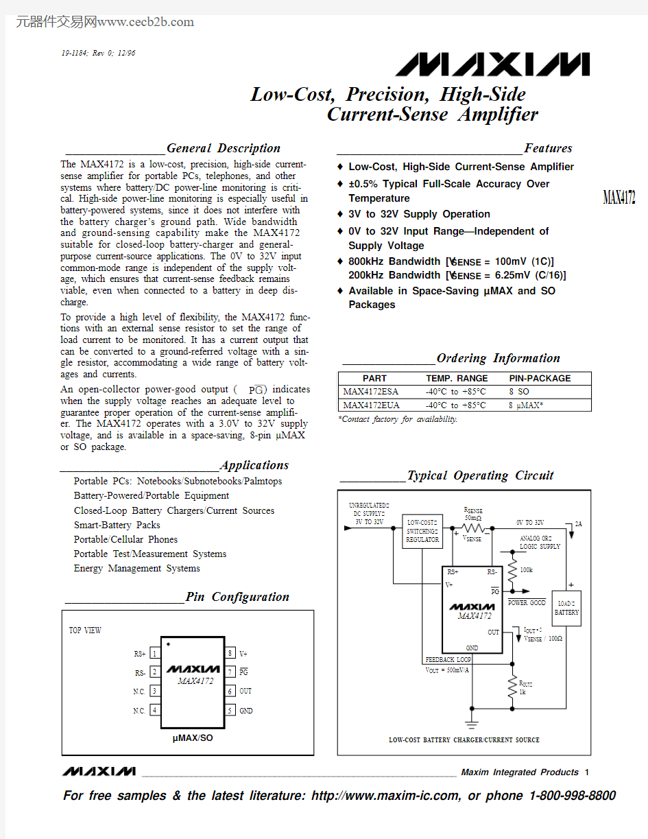
To provide a high level of flexibility, the MAX4172 func-tions with an external sense resistor to set the range of load current to be monitored. It has a current output that can be converted to a ground-referred voltage with a sin-gle resistor, accommodating a wide range of battery volt-ages and currents.
An open-collector power-good output (PG ) indicates when the supply voltage reaches an adequate level to guarantee proper operation of the current-sense amplifi-er. The MAX4172 operates with a 3.0V to 32V supply voltage, and is available in a space-saving, 8-pin μMAX or SO package.
________________________Applications
Portable PCs: Notebooks/Subnotebooks/Palmtops Battery-Powered/Portable Equipment
Closed-Loop Battery Chargers/Current Sources Smart-Battery Packs Portable/Cellular Phones
Portable Test/Measurement Systems Energy Management Systems
____________________________Features
o Low-Cost, High-Side Current-Sense Amplifier o ±0.5% Typical Full-Scale Accuracy Over Temperature o 3V to 32V Supply Operation
o 0V to 32V Input Range—Independent of Supply Voltage o 800kHz Bandwidth [V SENSE = 100mV (1C)]200kHz Bandwidth [V SENSE = 6.25mV (C/16)]o Available in Space-Saving μMAX and SO Packages
MAX4172
Low-Cost, Precision, High-Side
Current-Sense Amplifier
________________________________________________________________Maxim Integrated Products 1
__________________Pin Configuration
__________Typical Operating Circuit
19-1184; Rev 0; 12/96
For free samples & the latest literature: https://www.doczj.com/doc/2f18195023.html,, or phone 1-800-998-8800
*Contact factory for availability.
M A X 4172
Low-Cost, Precision, High-Side Current-Sense Amplifier 2_______________________________________________________________________________________
ABSOLUTE MAXIMUM RATINGS
ELECTRICAL CHARACTERISTICS
(V+ = +3V to +32V; RS+, RS- = 0V to 32V; T A = T MIN to T MAX ; unless otherwise noted. Typical values are at V+ = +12V, RS+ = 12V, T A = +25°C.)
Stresses beyond those listed under “Absolute Maximum Ratings” may cause permanent damage to the device. These are stress ratings only, and functional operation of the device at these or any other conditions beyond those indicated in the operational sections of the specifications is not implied. Exposure to absolute maximum rating conditions for extended periods may affect device reliability.
V+, RS+, RS-, PG ...................................................-0.3V to +36V OUT..............................................................-0.3V to (V+ + 0.3V)Differential Input Voltage, V RS+- V RS-............................±700mV Current into Any Pin..........................................................±50mA Continuous Power Dissipation (T A = +70°C)
SO (derate 5.88mW/°C above +70°C)..........................471mW μMAX (derate 4.10mW/°C above +70°C).....................330mW
Operating Temperature Range
MAX4172E_A....................................................-40°C to +85°C Storage Temperature Range.............................-65°C to +150°C Lead Temperature (soldering, 10sec).............................+300°C
ELECTRICAL CHARACTERISTICS (continued)
(V+ = +3V to +32V; RS+, RS- = 0V to 32V; T A = T MIN to T MAX ; unless otherwise noted. Typical values are at V+ = +12V, RS+ = 12V, T A = +25°C.)
MAX4172
Low-Cost, Precision, High-Side
Current-Sense Amplifier
_______________________________________________________________________________________3
1000950500
10
SUPPLY CURRENT vs. SUPPLY VOLTAGE
600650550900850800
V+ (V)
S U P P L Y C U R R E N T (μA )
203075070040
0.50.4-0.5
10
OUTPUT ERROR vs. SUPPLY VOLTAGE
-0.3
-0.4-0.20.30.20.1V+ (V)
E R R O R (%)
2030
0-0.140
1.5
1.0-3.0
10
C/16 LOAD OUTPUT ERROR vs. SUPPLY VOLTAGE
-2.0-1.5
-2.50.50V+ (V)
E R R O R (%)
2030
-0.5-1.040
__________________________________________Typical Operating Characteristics
(V+ = +12V, V RS+= 12V, R OUT = 1k ?, T A = +25°C, unless otherwise noted.)
Note 1:6.25mV = 1/16 of typical full-scale sense voltage (C/16).
Note 2:Valid operation of the MAX4172 is guaranteed by design when PG is low.
0.750.55-0.65
6
30
40OUTPUT ERROR
vs. COMMON-MODE VOLTAGE
-0.45-0.250.350.15
V RS- (V)
E R R O R (%)12
18-0.0524
2.95
2.902.45
-40-1585
V+ THRESHOLD FOR PG OUTPUT LOW
vs. TEMPERATURE
2.502.552.602.852.802.752.70TEMPERATURE (°C)
V + T R I P T H R E S H O L D (V )10352.656040-50.1m
10m 100m
1m
1
ERROR vs. SENSE VOLTAGE
0M A X 4172-04
V SENSE (V)
E R R O R (%)
10515202530
353500.010.11101001000
POWER-SUPPLY REJECTION RATIO
vs. FREQUENCY
5POWER-SUPPLY FREQUENCY (kHz)
E R R O R (%)
15102030
2510μs/div
0mV to 10mV V SENSE TRANSIENT RESPONSE
GND
V SENSE 5mV/div
V OUT 50mV/div
GND
MAX4172-08
10μs/div
0mV to 100mV V SENSE TRANSIENT RESPONSE
GND
V SENSE 50mV/div
V OUT 500mV/div
GND
MAX4172-09
M A X 4172
Low-Cost, Precision, High-Side Current-Sense Amplifier 4_______________________________________________________________________________________
____________________________Typical Operating Characteristics (continued)
(V+ = +12V, V RS+= 12V, R OUT = 1k ?, T A = +25°C, unless otherwise noted.)
MAX4172
Low-Cost, Precision, High-Side
Current-Sense Amplifier
_______________________________________________________________________________________5
5μs/div
START-UP DELAY
GND
V OUT 500mV/div
V+ 2V/div
GND
V SENSE = 100mV
MAX4172-10
10μs/div
V+ to PG POWER-UP DELAY
GND
PG 2V/div
V+ 2V/div
GND
100k ? PULL-UP RESISTOR FROM PG TO +4V
MAX4172-11
______________________________________________________________Pin Description
____________________________Typical Operating Characteristics (continued)
(V+ = +12V, V RS+= 12V, R OUT = 1k ?, T A = +25°C, unless otherwise noted.)
Current Output. OUT is proportional to the magnitude of the sense voltage (V RS+- V RS-). A 1k ?resistor from OUT to ground will result in a voltage equal to 10V/V of sense voltage.
OUT 6Power Good Open-Collector Logic Output. A low level indicates that V+ is sufficient to power the MAX4172, and adequate time has passed for power-on transients to settle out.PG 7Supply Voltage Input for the MAX4172
V+
8
Ground
GND 5No Connect. No internal connection. Leave open or connect to GND.N.C.3, 4PIN Load-side connection for the external sense resistor. The “-” indicates the direction of current flow.RS-2Power connection to the external sense resistor. The “+” indicates the direction of current flow.RS+1FUNCTION
NAME _______________Detailed Description
The MAX4172 is a unidirectional, high-side current-sense amplifier with an input common-mode range that is inde-pendent of supply voltage. This feature not only allows the monitoring of current flow into a battery in deep dis-charge, but also enables high-side current sensing at voltages far in excess of the supply voltage (V+).
The MAX4172 current-sense amplifier’s unique topolo-gy simplifies current monitoring and control. The MAX4172’s amplifier operates as shown in Figure 1.The battery/load current flows through the external sense resistor (R SENSE ), from the RS+ node to the RS-
node. Current flows through R G1and Q1, and into the current mirror, where it is multiplied by a factor of 50before appearing at OUT.
To analyze the circuit of Figure 1, assume that current flows from RS+ to RS-, and that OUT is connected to GND through a resistor. Since A1’s inverting input is high impedance, no current flows though R G2(neglect-ing the input bias current), so A1’s negative input is equal to V SOURCE - (I LOAD x R SENSE ). A1’s open-loop gain forces its positive input to essentially the same voltage level as the negative input. Therefore, the drop across R G1equals I LOAD x R SENSE . Then, since I RG1
M A X 4172
flows through R G1, I RG1x R G1= I LOAD x R SENSE . The internal current mirror multiplies I RG1by a factor of 50to give I OUT = 50 x I RG1. Substituting I OUT / 50 for I RG1,(I OUT / 50) x R G1 = I LOAD x R SENSE , or:
I OUT = 50 x I LOAD x (R SENSE / R G1)
The internal current gain of 50 and the factory-trimmed resistor R G1combine to result in the MAX4172transconductance (G m ) of 10mA/V. G m is de-fined as being equal to I OUT / (V RS+- V RS-). Since (V RS+- V RS-) = I LOAD x R SENSE , the output current (I OUT ) can be calculated with the following formula:
I OUT = G m x (V RS+- V RS-) =
(10mA/V) x (I LOAD x R SENSE )
Current Output
The output voltage equation for the MAX4172 is given below:
V OUT = (G m ) x (R SENSE x R OUT x I LOAD )
where V OUT = the desired full-scale output voltage,I LOAD = the full-scale current being sensed, R SENSE =the current-sense resistor, R OUT = the voltage-setting resistor, and G m = MAX4172 transconductance (10mA/V).
The full-scale output voltage range can be set by changing the R OUT resistor value, but the output volt-age must be no greater than V+ - 1.2V. The above equation can be modified to determine the R OUT required for a particular full-scale range:
R OUT = (V OUT ) / (I LOAD x R SENSE x G m )
OUT is a high-impedance current source that can be integrated by connecting it to a capacitive load.
PG Output
The PG output is an open-collector logic output that indicates the status of the MAX4172’s V+ power sup-ply. A logic low on the PG output indicates that V+ is sufficient to power the MAX4172. This level is tempera-ture dependent (see Typical Operating Characteristics graphs), and is typically 2.7V at room temperature. The internal PG comparator has a 100mV (typical) hystere-sis to prevent possible oscillations caused by repeated toggling of the PG output, making the device ideal for power-management systems lacking soft-start capabili-ty. An internal delay (15μs typical) in the PG compara-tor allows adequate time for power-on transients to settle out. The PG status indicator greatly simplifies the design of closed-loop systems by ensuring that the components in the control loop have sufficient voltage to operate correctly.
__________Applications Information
Suggested Component Values
for Various Applications
The Typical Operating Circuit is useful in a wide variety of applications. Table 1 shows suggested component values and indicates the resulting scale factors for vari-ous applications required to sense currents from 100mA to 10A.
Adjust the R SENSE value to monitor higher or lower cur-rent levels. Select R SENSE using the guidelines and for-mulas in the following section.
Sense Resistor, R SENSE
Choose R SENSE based on the following criteria:
?Voltage Loss:A high R SENSE value causes the
power-source voltage to degrade through IR loss.For minimal voltage loss, use the lowest R SENSE value.
Low-Cost, Precision, High-Side Current-Sense Amplifier
6_______________________________________________________________________________________
Figure 1. Functional Diagram
?
Accuracy:A high R SENSE value allows lower cur-rents to be measured more accurately. This is because offsets become less significant when the sense voltage is larger. For best performance,select R SENSE to provide approximately 100mV of sense voltage for the full-scale current in each application.
?Efficiency and Power Dissipation:At high current
levels, the I 2R losses in R SENSE can be significant.Take this into consideration when choosing the resistor value and its power dissipation (wattage)rating. Also, the sense resistor’s value might drift if it is allowed to heat up excessively.
?Inductance:Keep inductance low if I SENSE has a large high-frequency component. Wire-wound resis-tors have the highest inductance, while metal film is somewhat better. Low-inductance metal-film resis-tors are also available. Instead of being spiral wrapped around a core, as in metal-film or wire-wound resistors, they are a straight band of metal and are available in values under 1?.
?Cost:If the cost of R SENSE is an issue, you might
want to use an alternative solution, as shown in Figure 2. This solution uses the PC board traces to create a sense resistor. Because of the inaccura-cies of the copper resistor, the full-scale current value must be adjusted with a potentiometer. Also,copper’s resistance temperature coefficient is fairly high (approximately 0.4%/°C).
In Figure 2, assume that the load current to be mea-sured is 10A, and that you have determined a 0.3-inch-wide, 2-ounce copper to be appropriate. The resistivity of 0.1-inch-wide, 2-ounce (70μm thickness) copper is 30m ?/ft. For 10A, you might want R SENSE = 5m ?for a 50mV drop at full scale. This resistor requires about 2inches of 0.1-inch-wide copper trace.
Current-Sense Adjustment (Resistor Range, Output Adjust)
Choose R OUT after selecting R SENSE . Choose R OUT to obtain the full-scale voltage you require, given the full-scale I OUT determined by R SENSE . OUT’s high imped-ance permits using R OUT values up to 200k ?with minimal error. OUT’s load impedance (e.g., the input of an op amp or ADC) must be much greater than R OUT (e.g., 100 x R OUT ) to avoid degrading measurement accuracy.
High-Current Measurement
The MAX4172 can achieve high-current measurements by using low-value sense resistors, which can be paral-leled to further increase the current-sense limit. As an alternative, PC board traces can be adjusted over a wide range.
MAX4172
Low-Cost, Precision, High-Side
Current-Sense Amplifier
_______________________________________________________________________________________7
Table 1. Suggested Component Values
Figure 2. MAX4172 Connections Showing Use of PC Board
Maxim cannot assume responsibility for use of any circuitry other than circuitry entirely embodied in a Maxim product. No circuit patent licenses are implied. Maxim reserves the right to change the circuitry and specifications without notice at any time.
8___________________Maxim Integrated Products, 120 San Gabriel Drive, Sunnyvale, CA 94086 (408) 737-7600?1996 Maxim Integrated Products
Printed USA
is a registered trademark of Maxim Integrated Products.
M A X 4172
Low-Cost, Precision, High-Side Current-Sense Amplifier ___________________Chip Information
________________________________________________________Package Information
Power-Supply Bypassing and Grounding
In most applications, grounding the MAX4172 requires no special precautions. However, in high-current sys-tems, large voltage drops can develop across the ground plane, which can add to or subtract from V OUT .Use a single-point star ground for the highest current-measurement accuracy.
The MAX4172 requires no special bypassing and responds quickly to transient changes in line current. If the noise at OUT caused by these transients is a prob-lem, you can place a 1μF capacitor at the OUT pin to ground. You can also place a large capacitor at the RS terminal (or load side of the MAX4172) to decouple the load, reducing the current transients. These capacitors are not required for MAX4172 operation or stability. The RS+ and RS- inputs can be filtered by placing a capac-itor (e.g., 1μF) between them to average the sensed current.
TRANSISTOR COUNT: 177
SUBSTRATE CONNECTED TO GND