Silicon Photonic Waveguides and Devices for Near-and Mid-IR Applications Goran Z.Mashanovich,Frederic Y.Gardes,David J.Thomson,Youfang Hu,Ke Li,Member,IEEE, Milos Nedeljkovic,Jordi Soler Penades,Ali Z.Khokhar,Colin J.Mitchell,Stevan Stankovic,Rob Topley, Scott A.Reynolds,Yun Wang,Benedetto Troia,Vittorio M.N.Passaro,Senior Member,IEEE, Callum G.Littlejohns,Thalia Dominguez Bucio,Peter R.Wilson,Senior Member,IEEE,and Graham T.Reed
(Invited Paper)
Abstract—Silicon photonics has been a very buoyant research ?eld in the last several years mainly because of its potential for telecom and datacom applications.However,prospects of using sil-icon photonics for sensing in the mid-IR have also attracted interest lately.In this paper,we present our recent results on waveguide-based devices for near-and mid-infrared applications.The silicon-on-insulator platform can be used for wavelengths up to4μm; therefore,different solutions are needed for longer wavelengths. We show results on passive Si devices such as couplers,?lters,and multiplexers,particularly for extended wavelength regions and?-nally present integration of photonics and electronics integrated circuits for high-speed applications.
Index Terms—Silicon,infrared sensors,optical waveguides,op-tical?lters,optical resonators,photonic integrated circuits.
I.I NTRODUCTION
M ORE than a decade ago silicon photonics was seen as
a useful platform for passive photonic devices but there was skepticism about its viability for integrated optoelectronic circuits and systems.This skepticism mainly stemmed from sil-icon’s limitations for light emission and high speed optical mod-ulation in the telecommunication band.During the last decade, there have been numerous breakthroughs in the?eld,and today silicon photonics is seen as the leading candidate to circumvent the interconnect bottleneck problem.There are many research groups in the world,both in industry and academia,and several silicon photonics companies that offer commercial products on
Manuscript received October15,2014;revised November29,2014;accepted November30,2014.This work was supported in part by the EPSRC,U.K.under Grants U.K.Silicon Photonics,Silicon Photonics for Future Systems,HERMES, and MIGRATION.It was also supported in part by the Royal Society through Goran Mashanovich’s University Research Fellowship.
G.Z.Mashanovich, F.Y.Gardes, D.J.Thomson,Y.Hu,K.Li,M. Nedeljkovic,J.Soler Penades,A.Z.Khokhar,C.J.Mitchell,S.Stankovic, R.Topley,S.A.Reynolds,Y.Wang,C.G.Littlejohns,T.D.Bucio,P.R. Wilson,and G.T.Reed are with the University of Southampton,Southampton SO171BJ,U.K.(e-mail:g.mashanovich@https://www.doczj.com/doc/2d17431734.html,; f.gardes@soton. https://www.doczj.com/doc/2d17431734.html,; d.thomson@https://www.doczj.com/doc/2d17431734.html,;Y.Hu@https://www.doczj.com/doc/2d17431734.html,;kl@https://www.doczj.com/doc/2d17431734.html,; M.Nedeljkovic@https://www.doczj.com/doc/2d17431734.html,;jsp1g12@https://www.doczj.com/doc/2d17431734.html,;a.z.khokhar@https://www.doczj.com/doc/2d17431734.html,;
C.J.Mitchell@https://www.doczj.com/doc/2d17431734.html,;S.Stankovic@https://www.doczj.com/doc/2d17431734.html,;R.topley@https://www.doczj.com/doc/2d17431734.html,; s.reynolds@https://www.doczj.com/doc/2d17431734.html,;yw11e13@https://www.doczj.com/doc/2d17431734.html,;cl4m11@https://www.doczj.com/doc/2d17431734.html,; tdb2g12@https://www.doczj.com/doc/2d17431734.html,;prw@https://www.doczj.com/doc/2d17431734.html,;g.reed@https://www.doczj.com/doc/2d17431734.html,).
B.Troia and V.M.N.Passaro are with the Politecnico di Bari,70125Bari, Italy(e-mail:benedetto.troia@poliba.it;vittorio.passaro@poliba.it).
Color versions of one or more of the?gures in this paper are available online at https://www.doczj.com/doc/2d17431734.html,.
Digital Object Identi?er10.1109/JSTQE.2014.2381469the market.Silicon photonics is one of the most buoyant re-search?elds at the moment with a huge potential for applications in telecommunications and data communications,but also in sensing.
Historically,much of the research was focused on telecom-munication wavelength bands,however silicon and germanium are transparent up to8and15μm,respectively,thus offering a range of application in biochemical and environmental sens-ing,medicine,astronomy and communications[1].The major problem with a transition to the mid-infrared(MIR,2–20μm) is that the most dominant platform,that of silicon-on-insulator (SOI),can be used only up to4μm due to the high absorp-tion loss of silicon dioxide,and therefore alternative material platforms have to be utilized for longer wavelengths[1].How-ever,even in the near-infrared(NIR),where many groups use a220nm SOI platform,research teams have reported devices and integrated circuits based on different thickness’of both Si and buried oxide(BOX)layer.Xu et al.argue that there is a reason to revisit the choice of the SOI thickness because several Si photonic devices can perform better if thicker SOI is used rather than220nm SOI[2].For example,~300nm overlayer thicknesses are preferable for supporting TM polarization and hence for sensing applications.Directionality of grating cou-plers is found to be optimized for silicon thickness of350nm, whilst for optical modulators the authors have found thickness of360nm to give a maximum?gure of merit[2].To fully exploit the transparency range of SOI,400or500nm thick ovelayers need to be used.In addition,photonic SOI platforms usually have rather thick BOX to isolate the optical mode from the sub-strate,a structure that is not compatible with microelectronics. Therefore,C.Sun et al.,have developed a solution with inte-grated electronic circuits and suspended silicon waveguides in bulk silicon[3].Zimmerman et al.reported integration of an optical modulator and driver in a BiCMOS process which com-bined both SOI,for optical devices,and bulk Si for electronics [4].
In this paper we present our recent results on waveguides, splitters,interferometers,and?lters designed for the MIR.We investigate different material platforms,such as400and500nm SOI,and also suspended Si,and Ge-on-Si that offer extended transmission range in the MIR.Furthermore,for the more es-tablished NIR silicon photonics,we show grating couplers suit-able for wafer scale testing,record low loss echelle grating
1077-260X?2014IEEE.Personal use is permitted,but republication/redistribution requires IEEE permission.
See https://www.doczj.com/doc/2d17431734.html,/publications standards/publications/rights/index.html for more information.
multiplexers and a cost effective realization of photonic-electronic integrated circuits via wire bonding.
II.G ROUP IV W A VEGUIDES AND D EVICES FOR THE M ID-IR A.SOI Strip Waveguides and Passive Devices
The most dominant platform in silicon photonics has been SOI.A buried oxide layer with typical thickness of1–2μm is sandwiched between the top guiding Si layer and Si sub-strate.Different SOI thicknesses have been reported in literature and used by foundries.Established silicon photonics foundries such as IMEC and IME,have converged to using SOI wafers with220nm thick Si for their multi-project wafer runs[5]. Passive components,modulators and Ge photodetectors(PDs) are offered on this platform.The propagation losses as low as 0.6dB/cm have been reported for220nm thick strip SOI waveg-uides at1550nm and~2000nm.For shallow rib waveguides with70nm etch depth,the loss can be only0.1–0.2dB/cm[6]. Commercially available optical transceiver cables from Lux-tera/Molex are based on SOI with300–310nm thick Si,which was chosen to accommodate low loss compact passive devices and for a bulk-like transistor process[7],[8].Silicon photonics developments at Oracle and STMicroelectronics are also based on this platform[9],[10].We have already reported losses of ~1.5dB/cm for400nm rib SOI waveguides with220nm etch depth at a wavelength of3800nm[11].
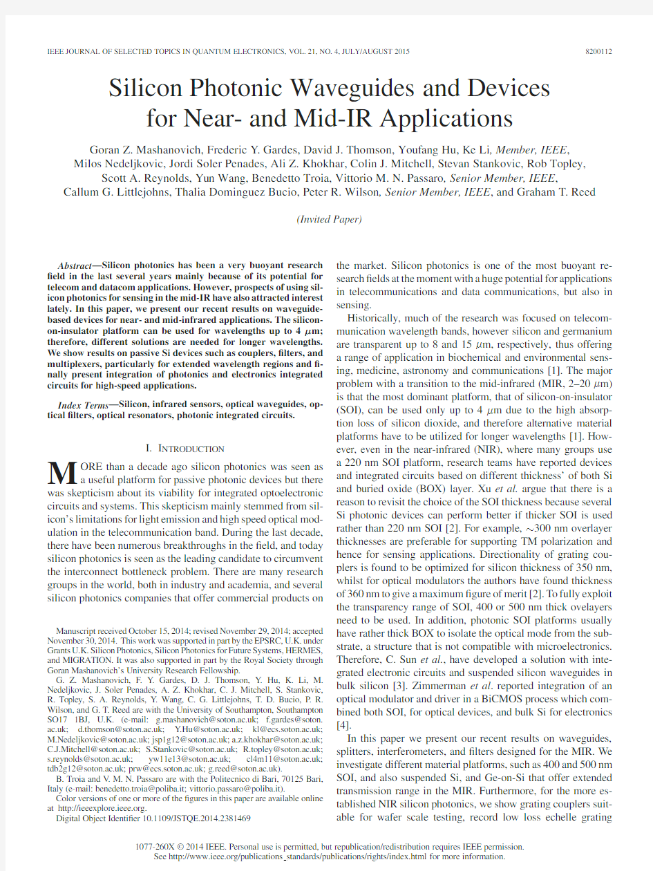
Here,we report results for500nm strip SOI waveguides at the same wavelength.The waveguides were fabricated by electron beam(e-beam)lithography and inductively coupled plasma(ICP)etching.Waveguides with different lengths but the same number of bends had surface grating couplers at both the input and output.A propagation loss of1.28±0.65dB/cm was measured for1.3μm wide waveguides using the cut back method.For1.1μm-wide strip waveguides the propagation loss was higher at2.72±0.57dB/cm,due to larger optical mode-sidewall interaction.These results are lower than previously reported results for400nm SOI waveguides[11],which is expected as the mode is more con?ned in silicon.
Micro?uidic channels can be integrated with waveguides for controlled interaction of a?uid analyte with a waveguide.Poly-dimethylsiloxane(PDMS)is a polymer that is widely used for the fabrication of micro?uidic channels,and so may be placed directly on top of waveguides.To estimate the loss that PDMS would introduce at3.8μm,the propagation loss section on the chip was covered with PDMS.The losses were5.44and 3.89dB/cm for1.1and1.3μm wide waveguides,respectively. In other words,additional loss of2.72and2.61dB/cm were introduced for1.1and1.3μm wide waveguides,respectively. That means,that a careful design of chips needs to be carried out to minimise the interaction of the optical mode with PDMS.In our future work,we will perform measurements at longer wave-lengths to assess viability of PDMS for sensing in the MIR. We have also developed multimode interference(MMI)split-ters on this platform.The MMIs were22.81μm long and8μm wide,and were connected via tapers with1.3μm and1.1μm wide input and output waveguides.Insertion losses of0.151±0.024and0.225±0.022dB/MMI were measured for
structures Fig.1.Insertion loss measurement at the wavelength of3.8μm of MMIs fab-
ricated on500nm SOI with1.1μm and1.3μm wide input/output
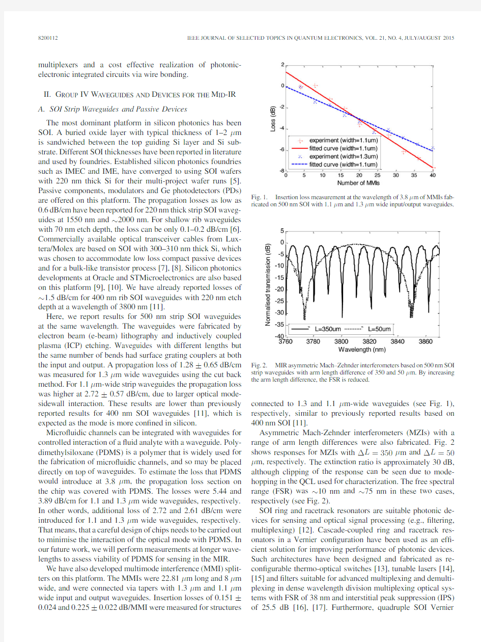
waveguides. Fig.2.MIR asymmetric Mach–Zehnder interferometers based on500nm SOI strip waveguides with arm length difference of350and50μm.By increasing
the arm length difference,the FSR is reduced.
connected to1.3and1.1μm-wide waveguides(see Fig.1), respectively,similar to previously reported results based on 400nm SOI[11].
Asymmetric Mach-Zehnder interferometers(MZIs)with a range of arm length differences were also fabricated.Fig.2 shows responses for MZIs withΔL=350μm andΔL=50μm,respectively.The extinction ratio is approximately30dB, although clipping of the response can be seen due to mode-hopping in the QCL used for characterization.The free spectral range(FSR)was~10nm and~75nm in these two cases, respectively(see Fig.2).
SOI ring and racetrack resonators are suitable photonic de-vices for sensing and optical signal processing(e.g.,?ltering, multiplexing)[12].Cascade-coupled ring and racetrack res-onators in a Vernier con?guration have been used as an ef?-cient solution for improving performance of photonic devices. Such architectures have been designed and fabricated as re-con?gurable thermo-optical switches[13],tunable lasers[14], [15]and?lters suitable for advanced multiplexing and demulti-plexing in dense wavelength division multiplexing optical sys-tems with FSR of38nm and interstitial peak suppression(IPS) of25.5dB[16],[17].Furthermore,quadruple SOI Vernier
MASHANOVICH et al.:SILICON PHOTONIC W A VEGUIDES AND DEVICES FOR NEAR-AND MID-IR APPLICATIONS8200112 TABLE I
D IMENSIONS OF F ABRICATED SOI V ERNIER D EVICES
Device L#1
(μm)L#2
(μm)
R#1
(μm)
R#2
(μm)
L i,#1
(μm)
L i,#2
(μm)
g0
(nm)
V#1919.1965.713013851.149.3400 V#2600.9636.3808549.151.1400 racetrack resonators have been proposed for enhancing?lter per-
formance,exhibiting a FSR of37.52nm with a IPS of~40dB
[18].In addition,thermally tunable microring optical?lters us-
ing p-i-p type microheaters have been proposed for enlarging the
FSR up to~95nm[19]and grating assisted-couplers have been
used to completely eliminate the FSR in the drop and through
port of the cascaded architecture[20].
The Vernier effect has been widely used for the design and
fabrication of high performance sensors in the NIR[e.g.21].
For example,experimental sensitivities of24300nm/RIU and
2430dB/RIU(RIU=refractive index unit)have been achieved
for wavelength and intensity interrogation,respectively[22].
The Vernier effect has been also investigated by cascading a ring
resonator with a MZI[23],and by exploring different technology
platforms such as silicon nitride microring resonators,[24]and
MZIs based on slot waveguides revealing a surface detection
limit as low as0.155pg/mm2[25].
Here,we present MIR Vernier con?gurations based on race-
track resonators fabricated on the500nm SOI platform with
a3μm BOX.A sophisticated algorithmic procedure based on
the Finite Element Method and Coupled Mode Theory was im-
plemented for the design of waveguides,directional couplers
as well as single and cascade-coupled racetrack resonators.The
strip waveguides were1300nm wide.
Two Vernier devices(V#1and V#2),were fabricated in an
architecture similar to that proposed in[26].Table I lists the
geometrical dimensions such as the racetrack lengths(L#1and
L#2),radii(R#1and R#2),interaction lengths of the symmetric
directional couplers(L i,#1and L i,#2)and directional coupler
gap,g0.
Subwavelength grating couplers were used to couple light
from a QCL to the chip via MIR optical?bres.The FSR of
racetrack resonators in V#1were around3.7nm(i.e.,FSR#1=
3.79nm,FSR#2=3.60nm,ΔFSR=190pm),insertion loss ~1.2dB,extinction ratio>22dB and Q factors3000–4400. Fig.3(a)shows the overall Vernier spectrum of the con?guration
labeled as V#1plotted on dB scale.Two entire Vernier patterns
made of close resonance peaks separated by a spectral distance
ΔλVernier≈4nm,were achieved in the3.72μm to3.88μm spectral window.An overall FSR Vernier equal to71.81nm was measured.
In Fig.3(b),the overall Vernier spectrum of the V#2con-
?guration is plotted on dB scale.As listed in Table I,Ring#1
and Ring#2of this con?guration were characterized by shorter
lengths,i.e.600.9and636.3μm,respectively.Consequently,
the FSRs of both resonators were larger than FSRs of single
microcavities of the con?guration V#1.In fact,FSR#1was
equal to5.8nm and FSR#2to5.48nm,givingΔFSR=320
pm.By using shorter racetrack resonator lengths,
parameters Fig.3.Normalized experimental and simulated transmittances of the Vernier architectures(a)V#1and(b)V#2.
TABLE II
E XPERIMENTAL O PTICAL P ARAMETERS O
F SOI V ERNIER D EVICES
Device FSR Vernier(nm)IL avg(dB)ER max(dB)G
V#171.81 3.8516.9719.94
V#299.32 2.3918.1918.12
ΔλVernier and FSR Vernier became larger,being equal to~6nm and99.32nm,respectively.This effect can be easily appreciated by comparing Vernier spectra in Fig.3(a)and(b),plotted in the same spectral window.
It is worth highlighting that in both spectra plotted in Fig.3, good agreement between the experimental and simulated spectra was achieved.Moreover,the shape of the resonances constitut-ing the Vernier peaks was not constant throughout the over-all experimental wavelength range.This effect was mainly due to wavelength dependence of input/output gratings and chro-matic dispersion affecting the operation of directional couplers as well as of cascade-coupled racetrack resonators.In conclu-sion,avarage insertion loss IL avg,maximum extiction ratio ER max and the Vernier gain G of the Vernier con?gurations V#1and V#2,are listed in Table II.
Using these con?gurations we have also demonstrated a Vernier sensor[27].
B.Slot Waveguides
Slot waveguides(see Fig.4)can enhance the electric?eld am-plitude in the gap region(up to50times higher[28])compared
8200112IEEE JOURNAL OF SELECTED TOPICS IN QUANTUM ELECTRONICS,VOL.21,NO.4,JULY/AUGUST
2015
Fig.4.Mode pro?le of a SOI slot waveguide.A signi?cant part of the mode is in the air gap.
to standard waveguide structures and thus can provide increased sensitivity in future MIR silicon photonics sensors.Recent re-sults for this waveguide type in the NIR include SOI slot waveg-uides with loss of2.28±0.03dB/cm at1064nm[29]and 2dB/cm at1550nm[30].In the MIR,a propagation loss of 11dB/cm at3.4μm was reported for silicon-on-sapphire slot waveguides[31].In this sub-section we report a signi?cant im-provement compared to our work described in[11]where the reported loss at3.8μm was9dB/cm.
The simulation of the structure was performed using Photon Design Fimmprop FMM solver.The devices were fabricated using e-beam lithography and ICP etching on150mm SOI wafers with a2μm BOX and400nm silicon overlayer.The slot waveguides were1.47μm wide with a70nm slot width. Light from a QCL is coupled to rib waveguides via surface grating couplers and then from rib to slot waveguides via a taper termination proposed in[30].The width of the rib waveguides was1.35μm and etch depth220nm.The slot waveguides were not fully,but partially etched to the same etch depth as the rib waveguides.
The propagation loss of the slot waveguides measured was 2.6±0.24dB/cm whilst the rib-slot transition loss was 0.03dB/interface.Bends with60μm radius had loss of 0.082dB/90°bend.Further reduction of the loss could be achieved by sidewall smoothing using thermal oxidation,al-though this may also change the geometry of the interface and thus impact transmission.
C.Suspended Waveguides
In has been shown that the loss of SOI waveguides increases for wavelengths longer than3.7–3.8μm[32].In order to use the full transparency region of Si,the SiO2cladding needs to be replaced by a cladding with suitable transparency region,or the buried oxide layer should be removed leaving suspended Si waveguides.
The latter approach was implemented by Cheng et al.[33]. They demonstrated rib waveguides with etched holes in the slab region that served for HF removal of the buried oxide cladding.These holes were placed approximately3μm from the rib waveguide so as not to disturb the mode propagation. The minimum propagation loss measured at a wavelength of 2.75μm was around3dB/cm.The fabrication involved two etch steps,one for the formation of the rib waveguide and one for the holes in Si slab used for under-etching the
BOX.Fig.5.SEM of a suspended Si waveguides with subwavelength lateral gratings which act both as lateral claddings and access points for buried oxide removal. We have developed a novel design that requires one etch step for the formation of lateral holes(see Fig.5).These subwave-length holes have a twofold purpose:to create a lateral cladding and for removal of the buried oxide layer by HF etching.The design is also more robust than the one reported in[33]since the thickness of the Si overlayer is constant on the chip.The waveguides were1.1μm wide,the holes were3–5μm wide and we varied their duty cycles(hole/silicon width ratios).For a150nm/150nm ratio,liquid HF could not be used as the holes were too small.We used vapour phase HF instead,but the oxide etch was too slow.To solve this problem,we increased the subwavelength grating period to550nm,and increased the air/Si ratio to450/100nm.Liquid HF could then be used and we demonstrated propagation of MIR light through these suspended structures,with a minimum loss of3.6dB/cm at a wavelength of3.8μm[34].Light was coupled from MIR optical?bres via fully etched and suspended subwavelength grating couplers.Fu-ture work will include development of other passive structures in this platform.
D.Ge on Si Waveguides
To increase transparency of a group IV photonic platform further into the MIR,Ge can be used.Its transparency extends to15μm[1].Two micrometer thick strip Ge-on-Si waveguides with losses of~3dB/cm were?rst reported in[35].Similar losses for the same structure,at a similar wavelength range, were also reported by Malik et al.[36].These waveguides have also been characterised at a wavelength range of2–2.6μm[37]. The waveguides were fabricated by chemical vapour deposition (CVD)growth and reactive ion etching(RIE)using a metal mask.
We have designed Ge-on-Si rib waveguide platform for a wavelength of3.8μm(see Fig.6).The starting Ge-on-Si wafers were fabricated by epitaxially depositing a2μm thick Ge layer onto a Si substrate using CVD.To fabricate the rib waveguides a SiO2hard mask was de?ned,which was deposited via plasma enhanced CVD(PECVD),then patterned via contact lithogra-phy and RIE using an Ar/CHF3plasma.The photoresist was
MASHANOVICH et al.:SILICON PHOTONIC W A VEGUIDES AND DEVICES FOR NEAR-AND MID-IR APPLICATIONS
8200112
Fig.6.Ge-on-Si rib waveguide fabricated in the Southampton Nanofabrica-tion Centre.
subsequently stripped and a further RIE step performed (SF6/CHF3plasma)to form the waveguides.Finally,the SiO2 mask was removed using a HF bath and the samples were cleaned and cleaved.The waveguides used in this work were designed to have an etch depth of1.2μm and a core width of2.25μm.To facilitate coupling,input and output tapers were fabricated at each end with a maximum width of10μm.Waveg-uides of different lengths were incorporated on the chip by in-troducing four identical bends with radius of100μm.
The propagation loss of these waveguides was measured by the cut back method giving a loss of2.4±0.2dB/cm at a wavelength of3.8μm.We believe that this is the lowest reported loss for Ge on Si waveguides.Our future work will include the development of other passive and active devices on this platform,including grating couplers,splitters,interferometers, modulators and detectors.
III.E RASABLE G RATING C OUPLERS
Coupling of light into a sub-micron waveguide to be used alongside electronics is a non-trivial task.Planar waveguides are around two orders of magnitude smaller than a standard?-bre based waveguide leading to a large mode mismatch.The most popular approach is a surface grating coupler,?rst demon-strated by Dakss et al.[38].Grating couplers do not require time consuming preparation such as polishing or antire?ective coat-ings and can be measured before dicing the wafer,potentially allowing time and cost savings.They are formed by a periodic change in the effective index of the waveguide,typically by util-ising an etch process[39],[40].Light is then coupled in or out through the surface at an angle.
Grating couplers have moved on signi?cantly since their in-ception by Dakss et al.[38].Key optimisations can be made to increase the outcoupling ef?ciency of a grating coupler such as the addition of an overlayer to the grating region,which im-proves ef?ciency by increasing the directionality of the output ?eld as shown by Roelkens et al.[41].Although only55%ef?-ciency was demonstrated empirically it was suggested that80% ef?ciency should be attainable in such structures.Coupling ef?-ciency can also be increased by adding a substrate re?ector or by improving the mode overlap between the Gaussian optical?bre mode and the outcoupled grating mode.This can be achieved using apodization.Taillaert et al.provided an insightful publica-tion on these enhancements[39].A numerical optimisation was used to achieve a Gaussian output?eld pro?le from the grating coupler and a Bragg re?ector was added to the substrate.The simulated results showed that for a13μm device length,an ef?ciency of61%was achievable in SOI without the substrate Bragg re?ector and up to92%with the Bragg re?ector.The etch pro?le was still rectangular and without the Bragg mirror the complexity of the fabrication process was no different to typical uniform gratings,though the critical feature size would be smaller in the apodized design.Chen et al.provided some more recent apodized devices[42]claiming a coupling loss of only?1.2dB per coupler in the best devices corresponding to an ef?ciency of75.9%with a substrate re?ector,with devices without the re?ector achieving a coupling performance better than?2dB(63.1%).They also noted that apodization reduces back re?ection into the waveguide,which is highly desirable to reduce noise experienced by other integrated devices.Further work into this style of device has demonstrated the best grating coupling performance available in SOI to date,Zaoui et al.[43] demonstrated coupling loss results of only0.62dB(87%ef?-ciency)per coupler empirically using an apodized design along with an aluminium bottom re?ector.
Grating couplers also offer the ability to couple light into or out from a waveguide at intermediate points along the op-tical circuit,allowing for autonomous testing at a component level.However,grating couplers in the SOI platform are tradi-tionally fabricated using a surface relief approach which is not easily removable.Grating couplers formed using ion implan-tation however,can be removed after measurement using laser annealing[44].The ion implantation process introduces disor-der into the silicon lattice,typically in the form of vacancy and self-interstitial defects,which results in an increase in the refrac-tive index of the material.The magnitude of the refractive index increase is dependent on the level of disorder introduced to the lattice but can be an increase of almost0.6.Energy provided via a thermal processes such as oven based or laser annealing allows order to be restored to the lattice,and hence removing the associated refractive index change.Here,we describe the fabrication of gratings utilising the implantation technique and give experimental evidence of their performance.
The waveguide sections comprised a220nm thick Si wire waveguide with a400nm width to ensure single mode operation; the buried oxide layer had a thickness of2μm.The waveguide width was increased to10μm for the grating test point via a dual step taper to maximise the overlap integral between the ?bre mode and grating mode.
The?rst stage of the process was to fabricate waveguides on the Si layer.Subsequently an e-beam resist(ZEP520A)was spun onto the wafer at2000r/min in order to achieve a500nm resist thickness.E-beam lithography was used to pattern the grating into the resist,which was then developed,before the entire structure was implanted with germanium ions using a dose of1×1015ions cm?2to ensure amorphization[44].The implantation energy is varied depending on the required depth
8200112IEEE JOURNAL OF SELECTED TOPICS IN QUANTUM ELECTRONICS,VOL.21,NO.4,JULY/AUGUST2015
of amorphization,in this case an energy of100KeV was used. Following implantation the resist was removed using a three stage solvent clean of acetone,isopropanol and deionised water for2min per bath in the listed order,followed by a10min O2 plasma ashing process.
Following successful fabrication,the amorphous grating can be tested an unlimited number of times during other manufac-turing stages of the optical circuit.However,exposure to high temperatures(above500°C)may reduce coupling ef?ciency [45].After testing has been completed,the grating can be erased from the optical circuit via an annealing process.Annealing can either be carried out in an oven at a minimum temperature of 500°C or by a https://www.doczj.com/doc/2d17431734.html,ing oven annealing is not desirable as the heat applied may cause damage to other fabricated devices and therefore to the whole https://www.doczj.com/doc/2d17431734.html,ser annealing offers an advantageous localised annealing method which does not affect other fabricated devices.
It may be logical to assume that there is a drastic difference between implanted and surface relief grating couplers due to the signi?cant difference in both the refractive index contrast, and the differing pro?les between the two fabrication methods, but this is not the case.Five variations of the implanted grating were tested in total with grating periods of580,590,600,610, and620nm.All structures consisted of uniform gratings with a ZEP e-beam resist implant mask,with a duty cycle of50%. Germanium at an energy of100keV with a dose of1×1015 ions cm?2was implanted into Si.Surface relief grating couplers were also fabricated alongside the implanted couplers for use as a comparison to the implanted couplers.The period used for the surface relief gratings was700nm and the etch depth used was70nm.Simulation data suggested that the outcoupling ef?ciencies of the implanted gratings and surface relief gratings used in this work were45%and52%,respectively.
Before characterisation,the optical characteristics of the mea-surement setup were accounted for by normalising all of the results to a transmission measurement of the setup,using an optical?bre to bypass the grating couplers and optical device under test.The best implanted grating coupler demonstrates a loss of only5.5dB(28%coupling ef?ciency)compared with a loss of4.5dB(35%coupling ef?ciency)shown for a comparable surface relief grating coupler,a difference of only7%.Although the ef?ciency demonstrated is likely to be suf?cient for wafer scale testing,it is expected that performance obtained from the uniform implanted grating couplers could be improved signif-icantly using either apodization or by the addition of a bottom re?ector if necessary.The measured ef?ciency value is lower than the simulated value in both implanted and surface relief grating coupler cases,this is dominantly due to the difference in the modal overlap between the?bre mode and the mode exiting the grating coupler,though the difference between the measured results is in agreement with the difference expected from sim-ulations.This suggests that the implanted grating coupler does not possess any unexpected loss mechanisms compared with the surface relief fabrication method.
To enable a more detailed comparison between the implanted and the surface relief grating coupler’s characteristics we con-sider transmission data of both fabrication methods with
the https://www.doczj.com/doc/2d17431734.html,parison between the etched and implanted surface grating cou-plers.
same central wavelength,as shown in Fig7.At this central wavelength,the coupling loss of the implanted device increases to6.6dB.Interestingly at the peak of the output performance (within0.25dB of the maximum)the implanted coupler dis-plays a wider bandwidth than the surface relief grating coupler, with peak performance bandwidths of16and8nm,respectively. Typically the performance metric used for grating couplers is the bandwidth at1dB below peak performance.The1dB band-width of the implanted and surface relief couplers are almost identical at32and30nm,respectively.A1dB bandwidth of 30nm is comparable to uniform surface relief gratings published in the literature.This technology can in principle be translated into the MIR,however an investigation of the refractive index of ion implanted amorphous silicon would need to be measured at longer wavelengths.
IV.P LANAR C ONCA VE G RATINGS Wavelength division(de)multiplexers on SOI platform are important devices for integrated photonic circuits and can be realized by various structures,such as arrayed waveguide grat-ings(AWGs)[46],[47],cascaded Mach-Zehnder interferome-ters(cMZIs)[46],[48],angled multimode interferometers(AM-MIs)[49],[50],cascade ring resonators(cRRs)[46],[51],and planar concave gratings(PCGs)[46],[52]etc.Recent progress in silicon photonics has demonstrated AWGs,cMZIs and cRRs with low insertion loss,low cross talk,and?at-top spectral re-sponse.However,these WDM structures have phase shifters formed by sub-micron single mode waveguides,which require precise control of the waveguide width during fabrication.AM-MIs have also been demonstrated as WDM structures in various con?gurations.They are less sensitive to fabrication errors in waveguide width,whilst their channel count is limited to a small number(?4)[49]unless extra single mode waveguide based structures(e.g.MZI)are used for interleaving[50].PCGs can have more channels than MMIs and use micron-scale echelle gratings instead of submicron waveguides as dispersive struc-tures.They have an advantage that waveguide width control is
MASHANOVICH et al.:SILICON PHOTONIC W A VEGUIDES AND DEVICES FOR NEAR-AND MID-IR APPLICATIONS
8200112
Fig.8.SEM image of the fabricated Bragg re?ectors at the PCG
mirrors.
Fig.9.The schematic drawing of the fabrication process:step1-de?nition of the waveguide for the modulator;step2-de?nition of waveguide transition structure,input/output waveguides and Bragg mirrors of the PCG.
not required.The main challenge to achieve high-performance PCGs for low-insertion-loss and low-cross-talk operation is to minimise phase errors at both grating facets and slab areas.Here, we demonstrate a4-channel PCG with a thin slab waveguide on the SOI platform for the integration with a silicon modulator. An insertion loss of<1dB and a cross-talk of
The PCG was designed in a Roland circle con?guration and had a footprint of380μm by180μm excluding input/output waveguides.The PCG had41grating facets and each facet was a4-period Bragg re?ector with a period of340nm and a duty cycle of50%,(see Fig.8)which gave>95%re?ectivity over a wavelength band of100nm centred at1550nm.The silicon modulator to be integrated with the PCG had a400nm-wide rib shaped waveguide structure with a silicon overlay thick-ness of400nm and a slab thickness of180nm.Hence,we designed a PCG with a180nm-thick free propagation region (FPR),400nm by180nm stripe shaped input/output waveg-uides,and a waveguide transition structure to bridge the mod-ulator’s rib waveguides and the PCG’s stripe waveguide with low-loss power transfers(see Fig.9).
At the interfaces between the waveguide transitions and PCG’s input/output waveguides,the rib waveguide had a width of100nm,which was small enough and almost no mode power was contained in the100nm by220nm rib area.It was
designed Fig.10.Normalised transmission spectrum measured from a fabricated PCG. to smoothly“squeeze”the mode power from the rib area into the400nm by180nm slab area.
After the waveguide transition,the400nm wide input/output stripe waveguides were tapered up to a width of2μm before entering the FPR in order to suppress mode mismatch at the in-terfaces.In our design,the FPR had a thickness of only180nm, which was thin enough to guarantee single slab mode in the FPR and to make the Bragg mirror’s re?ectivity even more tolerant to the variation of vertical dimensions than that reported in[52]. Surface grating couplers with a period of570nm and a duty cycle of50%were used in the design to couple light from/to the single mode400nm/180nm rib waveguides.The surface grating couplers had a width of10μm and were connected to the single mode rib waveguides by adiabatic tapers.
The fabrication process is shown in the schematic drawing of Fig.9.Two lithography/etching steps were used.In the?rst step,the400nm/180rib waveguide was patterned.In the second step,the waveguide transition structure and the PCG mirrors with DBR re?ectors were patterned.In both steps,the structures were patterned by deep UV lithography and ICP etching.
The measured transmission spectra of a fabricated PCG is shown in Fig.10.The cross-talk across the four channels is approximately?20dB and the insertion loss for the4channels are1.0,0.7,1.7and1.7dB respectively.To the best of our knowledge,this is the lowest insertion loss achieved in PCGs on the SOI platform.
V.I NTEGRATION
Finally,after reporting various silicon photonics devices op-erating in the NIR and MIR,we show our results on integration of photonic and electronic circuits.In recent years,researchers have demonstrated silicon photonic transceiver links based on a vertical cavity surface emitting laser[53],ring resonator modu-lator[54]and a Mach-Zehnder modulator(MZM)[55],[56].Al-though the MZM approach has lower power ef?ciency compared to the other two approaches[57],the relatively large bandwidth and improved tolerance to process and temperature variations make it attractive for low cost silicon photonic transceivers.
8200112IEEE JOURNAL OF SELECTED TOPICS IN QUANTUM ELECTRONICS,VOL.21,NO.4,JULY/AUGUST
2015
Fig.11.Image of wire bonds between the CMOS driver ampli?er and the Mach–Zehnder modulator.
While it has been demonstrated that voltage mode transmit-ters generally have better power ef?ciency compared to current mode drivers[58],previous MZM drivers[56],[59],[60]are based on the current mode logic approach.The only voltage mode driver that is integrated with MZM was used with a for-ward biased p-i-n diode and formed a2Gb/s silicon photonic switch[61].Here,we present a transmitter printed-circuit board (PCB),which consists of a carrier depletion based Si MZM and a voltage mode10Gb/s driver in a standard130nm CMOS pro-cess.To the best of our knowledge,this is the?rst voltage mode driver that is designed to be integrated with the reverse biased PN MZM.In addition,a separate receiver PCB consisting of a Ge-on-Si PD and a130nm CMOS transimpedance ampli?er (TIA)has also been implemented.The full link operation is also demonstrated up to10Gb/s.
The proposed design was fabricated using the IBM8RF 130nm CMOS process in bulk Si.The layout was designed for four parallel channels.The main circuit blocks were evenly distributed along the length of the chip,so as to?t the require-ments of I/O pads with a150μm pitch.A photograph showing the wire bonds between the driver chip,MZM chip and the PCB is shown in Fig.11.The input differential electrical sig-nal was connected onto the FR4printed circuit board via two SMA connectors and microstrip lines routed to the input side of the CMOS driver chip.Wire bonds were then used to connect onto the CMOS driver chip.On the output side of the driver chip wire bonds were again used to connect the ampli?ed differential electrical data to the input of the MZM modulator.DC power was also applied to the PCB where it was regulated before being passed to the driver chip again via wire bonds.Input and out-put light was coupled to and from the modulator using surface grating couplers.
The optical modulator was fabricated in220nm SOI and has been described previously[62].The waveguide dimensions were400nm width,220nm height and100nm slab height.The device was based upon free carrier depletion of a pn junction which is self-aligned with one edge of the rib waveguide.The phase modulator was formed in both arms of a MZI to balance the losses and to allow for push-pull operation.Coplanar
wave-Fig.12.Image of wire bonds between the CMOS TIA and the PD.
guide electrodes were used to propagate the high speed data signal along the phase modulators.At the inputs of the CPW electrodes the signal lines were widened to allow wire bonding. The receiver side was developed using a similar approach. Fig.12shows the wire bonds between the TIA chip and the PD chip and PCB.The input optical signal was launched onto the PD chip via a surface grating and propagated to a Ge based PD via a Si wire waveguide.The PD itself was based on a standard epixfab design.Wire bonds were then used to connect between the PD chip and the CMOS TIA chip.On the output side of the TIA wire bonds were used to connect the differential electrical data signal to the PCB where it propagated along microstrip lines to two output SMA connectors.DC power was again applied to the PCB where it was regulated and then connected to the TIA via further wire bonds.
The CMOS inverter TIA structure was adopted,with the ad-vantages of higher gain and relative lower noise[63].Some modi?cations made were that NMOS and PMOS transistors were seen with different feedback resistors,due to the trans-conductance of these devices being inherently different.The total receiver circuit consisted of a TIA,a10stage limiting am-pli?er,a single to differential converter and an output buffer. They were fabricated using the same IBM8RF130nm process as the driver,with a four parallel channel con?guration.The power consumption of each channel was~97.4mW.
In order to test the optical performance of the driver board, the light from a tunable laser was passed via optical?bre to the input coupler on the MZM chip.High speed data signals of up to10Gb/s were passed via COAX cable from the generator to the transmitter board.Electrical phase shifters were used to counter electrical timing mismatches introduced by the COAX cables.Light was coupled from the output of the MZM to an-other optical?bre which was passed to an erbium doped?bre ampli?er.The light was then passed to the DCA via a tunable band pass optical?lter.Open optical eye diagrams up to10Gb/s were observed.An eye diagram at8Gb/s can be seen in Fig.13 showing an extinction ratio of11dB.A power consumption of 465mW per channel was measured.This compares favourably with previously reported integrated transmitters based upon Si MZM where the power consumption has been stated.In[64]
MASHANOVICH et al.:SILICON PHOTONIC W A VEGUIDES AND DEVICES FOR NEAR-AND MID-IR APPLICATIONS
8200112
Fig.13.Eye diagram for integrated optical driver at8Gb/s.
front end integration of a silicon MZM and driver in BiCMOS was reported with operation at10Gbit/s and a power consump-tion of830mW.In[56]a power consumption of575mW was reported from a10Gbit/s transmitter based upon the front end integration of a Si MZM in CMOS.In[65]a wire bond inte-grated driver and QPSK modulator operating at28Gbaud with a power consumption of500mW was reported.In this case a SIS-CAP modulator was used rather than a carrier depletion based device and as a result a lower drive voltage is required.Trans-mitters with lower power consumption are possible when driver ampli?ers are integrated with ring resonator based modulators, however the optical bandwidth of the device is much reduced. In addition to this tuning is required to correctly position the resonance which shifts signi?cantly due to high fabrication and temperature sensitivities.This adds complexity and would also contribute to the power consumption of the transmitter.
The receiver board was tested by applying an optical data signal directly to the PD chip.The optical data signal was gen-erated by passing CW laser light through a commercial LiNbO3 modulator driven by a pseudorandom binary sequence genera-tor and commercial driver ampli?er.The light was then passed via an optical?bre to the PD chip.The electrical output data was passed via COAX cable to the electrical input of the DCA. Open electrical eye diagrams were obtained at8Gb/s and10 Gb/s.Fig.14shows an8Gb/s open eye diagram.The amplitude of the output electrical signal was approximately290mV.The supply voltage to the TIA was1.5V,drawn current64.2mA and therefore power consumption96.3mW.
Finally the full link was tested by connecting the ampli?ed optical output of the transmitted board to the optical input of the receiver board.The electrical data from the receiver board was passed to the DCA again via COAX cables.The resulting electrical eye diagram at8Gb/s is shown in Fig.15.
VI.C ONCLUSION
We have brie?y reviewed our recent results on waveguides for both near-and mid-IR wavelength bands.We have shown that low loss mid-IR waveguides,splitters and interferometers can be realised in SOI,suspended Si,and Ge-on-Si material plat-forms.Ge-on-Si has the largest transparency range of the three and with other advantages of Ge compared to Si,it has a lot
of Fig.14.Results of testing TIA at8
Gb/s.
Fig.15.Eye diagram for full link operating at8Gb/s.
promise for high speed communications and sensing applica-tions in the mid-IR.We have also presented erasable gratings in Si that can?nd application in wafer scale testing,record low loss echelle gratings with a minimum insertion loss of0.7dB,and cost-effective integration of photonic and electronic chips us-ing wire bonding.The modulator/detector chips were optimised and fabricated separately from the driver/TIA chips and the two were wire bonded.The maximum speed of an optical link com-prising an integrated transmitter and an integrated receiver was 10Gb/s.
A CKNOWLEDGMENT
The authors would like to thank C.A.Ramos,P.Cheben,A. O.Monux,and I.M.Fernandez for the modeling of suspended silicon waveguides,and N.Healy,S.Mailis and A.C.Peacock for the annealing of implanted gratings.
R EFERENCES
[1]R.Soref,“Mid-infrared photonics in silicon and germanium,”Nat.Pho-
ton.,vol.4,no.8,pp.495–497,Aug.2010.
[2] D.-X.Xu et al.,“Silicon photonics integration platform—Have we found
the sweet spot?,”IEEE J.Sel.Top.Quantum Electron.,vol.20,no.4,art.
no.8100217,Jul.-Aug.2014.
[3] C.Sun et al.,“A monolithically-integrated chip-to-chip optical link in
bulk CMOS,”in Proc.Digest IEEE Symp.Very Large Scale Integration Circuits,Honolulu,HI,USA,2014,pp.1–2.
8200112IEEE JOURNAL OF SELECTED TOPICS IN QUANTUM ELECTRONICS,VOL.21,NO.4,JULY/AUGUST2015
[4] D.J.Thomson et al.,“Silicon carrier depletion modulator with10Gbit/s
driver realized in high-performance photonic BiCMOS,”Laser Photon.
Rev.,vol.8,pp.180–187,2014.
[5] A.E.-J.Lim et al.,“Review of silicon foundry efforts,”IEEE J.Sel.Top.
Quantum Electron..,vol.20,no.4,art.no.8300112,Jul.-Aug.2014. [6]G.Roelkens,“Photonic integration:beyond telecom and datacom,”pre-
sented at the Eur.Conf.Interventional Oncol.,Nice,France,Paper Tu1, 2014.
[7] A.Mekis et al.,“Scaling CMOS photonics transceivers beyond100Gb/s,”
Proc.SPIE,vol.8265,pp.82650A–82658,2012.
[8] F.Boeuf et al.,“A Multi-wavelength3D-compatible silicon photonics
platform on300mm SOI wafers for25Gb/s applications,”presented at the Int.Electron.Devices Meeting,2013,Paper13.3.
[9] A.V.Krishnamoorthy et al.,“Exploiting CMOS manufacturing to reduce
tuning requirements for resonant optical devices,”IEEE Photon.J.,vol.
3,no.3,pp.567–579,Jun.2011.
[10] F.Boeuf,“Recent progress on silicon photonics R&D and manufacturing
on300mm wafer platform,”presented at the IEEE Group IV Photon., Paris,France,Paper WA2,2014.
[11]M.Nedeljkovic et al.,“Silicon photonic devices and platforms for the
mid-infrared,”Opt.Mater.Exp.,vol.3,pp.1205–1214,2013.
[12]V.M.N.Passaro,B.Troia,https://www.doczj.com/doc/2d17431734.html, Notte,and F.De Leonardis,“Photonic
resonant microcavities for chemical and biochemical sensing,”RSC Adv., vol.3,no.1,pp.25–44,2013.
[13]W.S.Fegadolli et al.,“Recon?gurable silicon thermo-optical ring res-
onator based on the Vernier effect control,”Opt.Exp.,vol.20,no.13,pp.
14722–14733,2012.
[14]J.C.Hulme,J.K.Doylend,and J.E.Bowers,“Widely tunable Vernier
ring laser on hybrid silicon,”Opt.Exp.,vol.21,no.17,pp.19718–19722, 2013.
[15]J.H.Lee et al.,“High power and widely tunable Si hybrid external-cavity
laser for power ef?cient Si photonics WDM links,”Opt.Exp.,vol.22,no.
7,pp.7678–7685,2014.
[16]R.Boeck,N.A.F.Jaeger,N.Rouger,and L.Chrostowski,“Series-coupled
silicon racetrack resonators and the Vernier effect:Theory and measure-ment,”Opt.Exp.,vol.18,no.24,pp.25151–25157,2010.
[17]R.Boeck et al.,“High performance Vernier racetrack resonators,”Opt.
Lett.,vol.37,no.24,pp.5199–5201,2012.
[18]R.Boeck,J.Flueckiger,L.Chrostowski,and N.A.F.Jaeger,“Experi-
mental performance of DWDM quadruple Vernier racetrack resonators,”
Opt.Exp.,vol.21,no.7,pp.9103–9112,2013.
[19]L.Zhou,X.Zhang,L.Lu,and J.Chen,“Tunable Vernier microring optical
?lters with p-i-p type microheaters,”IEEE Photon.J.,vol.5,no.4,art.
no.6601211,Aug.2013.
[20]R.Boeck,W.Shi,L.Chrostowski,and N.A.F.Jaeger,“FSR-eliminated
Vernier racetrack resonators using grating-assisted couplers,”IEEE Pho-ton.J.,vol.5,no.5,art.no.2202511,Oct.2013.
[21]https://www.doczj.com/doc/2d17431734.html, Notte et al.,“Recent advances in gas and chemical detection by
Vernier effect-based photonic sensors,”Sensors,vol.14,no.3,pp.4831–4855,2014.
[22]X.Jiang et al.,“Cascaded silicon-on-insulator double-ring sensors op-
erating in high-sensitivity transverse-magnetic mode,”Opt.Lett.,vol.38, no.8,pp.1349–1351,2013.
[23]https://www.doczj.com/doc/2d17431734.html, Notte and V.M.N.Passaro,“Ultra high sensitivity chemical pho-
tonic sensing by Mach-Zehnder interferometer enhanced Vernier-effect,”
Sens.Actuators B,Chem.,vol.176,pp.994–1007,2013.
[24]V.Zamora,P.L¨u tzow,M.Weiland,and D.Pergande,“Investigation of
cascaded SiN microring resonators at1.3μm and1.5μm,”Opt.Exp.,vol.
21,no.23,pp.27550–27557,2013.
[25]X.Tu et al.,“Thermal independent Silicon-Nitride slot waveguide biosen-
sor with high sensitivity,”Opt.Exp.,vol.20,no.3,pp.2640–2648, 2012.
[26] B.Troia et al.,“Cascade-coupled racetrack resonators based on the Vernier
effect in the mid-infrared,”Opt.Exp.,vol.22,pp.23990–24003,2014.
[27]G.Z.Mashanovich et al.,“Mid-infrared silicon photonics,”to be presented
at SPIE Photonics West2015,San Francisco,CA,USA,Feb.7-12,2015.
[28]P.T.Lin et al.,“Mid-infrared spectrometer using opto-nano?uidic slot-
waveguide for label-free on-chip chemical sensing,”Nano Lett.,vol.14, no.1,pp.231–238,2014.
[29]X.Li et al.,“Experimental demonstration of silicon slot waveguide with
low transmission loss at1064nm,”https://www.doczj.com/doc/2d17431734.html,mun.,vol.329,pp.168–172, 2014.
[30]Z.Wang et al.,“Ultra-compact low-loss coupler between strip and slot
waveguides,”Opt.Lett.vol.34,pp.1498–1500,2009.
[31]Y.Zou et al.,“Grating-coupled silicon-on-sapphire integrated slot waveg-
uides operating at mid-infrared wavelengths,”Opt.Lett.,vol.39,3070–3073,2014.[32]M.Muneeb et al.,“Demonstration of silicon-on-insulator mid-infrared
spectrometers operating at3.8μm,”Opt.Exp.,vol.21,pp.11659–11669, 2013.
[33]Z.Cheng et al.,“Focusing subwavelength grating coupler for mid-infrared
suspended membrane waveguide,”Opt.Lett.,vol.37,pp.1217–1219, 2012.
[34]J.Soler Penades et al.,“Suspended SOI waveguide with sub-wavelength
grating cladding for mid-infrared,”Opt.Lett.,vol.39,pp.5661–5664, 2014.
[35]Y.-C.Chang et al.,“Low-loss germanium strip waveguides on silicon for
the mid-infrared,”Opt.Lett.,vol.37,pp.2883–2885,2012.
[36] A.Malik et al.,“Germanium-on-silicon mid-infrared arrayed waveguide
grating multiplexers,”IEEE Photon.Technol.Lett.,vol.25,no.18,pp.
1805–1808,Sep.2013.
[37]G.Roelkens et al.,“Silicon-based heterogeneous photonic integrated
circuits for the mid-infrared,”Opt.Mat.Exp.,vol.3,pp.1523–1536, 2013.
[38]M.L.Dakss,L.Kuhn,P.F.Heidrich,and B.A.Scott,“Grating coupler
for ef?cient excitation of optical guided waves in thin?lms,”Appl.Phys.
Lett.,vol.16,pp.523–525,1970.
[39] D.Taillaert,P.Bienstman,and R.Baets,“Compact ef?cient broadband
grating coupler for silicon-on-insulator waveguides,”Opt.Lett.,vol.29, pp.2749–2751,2004.
[40]L.Vivien et al.,“Light injection in SOI microwaveguides using high-
ef?ciency grating couplers,”J.Lightw.Technol.,vol.24,no.10,pp.3810–3815,Oct.2006.
[41]G.Roelkens et al.,“High ef?ciency diffractive grating couplers for inter-
facing a single mode optical?ber with a nanophotonic silicon-on-insulator waveguide circuit,”Appl.Phys.Lett.,vol.92,pp.131101-1–131101-3, 2008.
[42]X.Chen et al.,“Apodized waveguide grating couplers for ef?cient cou-
pling to optical?bers,”IEEE Photon.Technol.Lett.,vol.22,no.15,pp.
1156–1158,Aug.2010.
[43]W.S.Zaoui et al.,“Bridging the gap between optical?bers and silicon
photonic integrated circuits,”Opt.Exp.,vol.22,pp.1277–1286,Jan.2014.
[44]R.Topley et al.,“Planar surface implanted diffractive grating couplers in
SOI,”Opt.Exp.,vol.22,pp.1077–1084,Jan.2014.
[45]R.Loiacono,“Erasable Bragg gratings in Silicon on insulator,”Ph.D.
dissertation,Dept.Electron.,Adv.Technol.Inst.,Surrey Univ.,Guildford, U.K.,2010.
[46]W.Bogaerts et al.,“Silicon-on-insulator spectral?lters fabricated with
CMOS technology,”IEEE J.Sel.Top.Quantum Electron.,vol.16,no.1, pp.33–44,Jan.-Feb.2010.
[47]J.Wang et al.,“Low-loss and low-crosstalk8×8silicon nanowire
AWG routers fabricated with CMOS technology,”Opt.Exp.,vol.22,pp.
9395–9403,2014.
[48]N.-N.Feng et al.,“Low-loss polarization-insensitive silicon-on-insulator-
based WDM?lter for triplexer applications,”IEEE Photon.Technol.Lett., vol.20,no.23,pp.1968–1970,Dec.2008.
[49]Y.Hu et al.,“Wavelength division(de)multiplexing based on waveguide
mode dispersion,”Opt.Lett.,vol.36,pp.4488–4490,2011.
[50]Y.Hu et al.,“Coarse wavelength division(de)multiplexer using inter-
leaved angled multimode interferometer structure,”Appl.Phys.Lett.,vol.
102,pp.251116–1–251116-4,2013.
[51]P.De Heyn et al.,“Fabrication-tolerant four-channel wavelength-division-
multiplexing?lter based on collectively tuned Si microrings,”J.Lightw.
Technol.,vol.31,no.16,pp.2785–2792,Aug.2013.
[52]J.Brouckaert et al.,“Planar concave grating demultiplexer with high
re?ective Bragg re?ector facets,”IEEE Photon.Technol.Lett.,vol.20,no.
4,pp.309–311,Feb.2008.
[53] C.Kromer et al.,“A100mW4×10Gb/s transceiver in80nm CMOS
for high-density optical interconnects,”IEEE J.Solid State Circuits,vol.
40,no.12,pp.2667–2679,Dec.2005.
[54]X.Zheng et al.,“Ultra-ef?cient10Gb/s hybrid integrated silicon photonic
transmitter and receiver,”Opt.Exp.,vol.19,no.6,pp.5172–5186,Mar.
2011.
[55] B.Analui,D.Guckenberger,D.Kucharski,and A.Narasimha,“A fully
integrated20-Gb/s optoelectronic transceiver implemented in a standard
0.13-μm CMOS SOI technology,”IEEE J.Solid State Circuits,vol.41,
no.12,pp.2945–2955,Dec.2006.
[56] A.Narasimha et al.,“A fully integrated4x10-Gb/s DWDM optoelec-
tronic transceiver implemented in a standard0.13μm CMOS SOI tech-nology,”IEEE J.Solid State Circuits,vol.42,no.12,pp.2736–2744,Dec.
2007.
[57] A.Palaniappan and S.Palerm,“Power ef?ciency comparisons of inter-
chip optical interconnect architectures,”IEEE Trans.Circuit Syst.-II,Exp.
Briefs,vol.57,no.5,pp.343–347,Mar.2010.
MASHANOVICH et al.:SILICON PHOTONIC W A VEGUIDES AND DEVICES FOR NEAR-AND MID-IR APPLICATIONS8200112
[58]S.Kim et al.,“A5.2Gb/s low-swing voltage-mode transmitter with an
AC-DC-coupled equalizer and a voltage offset generator,”IEEE Trans.
Circuit Syst.-I,Reg.Papers,vol.61,no.1,pp.213–225,Jan.2014. [59]K.Joohwa and J.F.Buckwalter,“A40Gb/s optical tranceiver front-end in
45nm SOI CMOS,”IEEE J.Solid State Circuits,vol.47,no.3,pp.1–4, Mar.2010.
[60]M.-S.Kao,F.-T.Chen,Y.-H.Hau,and J.-M.Wu,“20-Gb/s CMOS EA/MZ
modulator driver with intrinsic parasitic feedback network,”IEEE Trans.
Very Large Scale Integration Syst.,vol.22,no.3,pp.475–483,Mar.2014.
[61] B.G.Lee et al.,“Demonstration of digital CMOS driver codesigned and
integrated with broadband silicon photonic switch,”J.Lightw.Technol., vol.29,no.8,pp.1136–1142,Apr.2011.
[62] D.J.Thomson et al.,“High contrast40Gbit/s optical modulation in
Silicon,”Opt.Exp.,vol.19,no.12,pp.11507–11516,Jun.2011. [63]T.Chalvatvis et al.,“Low voltage topologies for40-Gb/s circuit in
nanoscale CMOS,”IEEE J.Solid State Circuits,vol.42,no.7,pp.1564–1573,Dec.2007.
[64]L.Zimmermann et al.,“Monolithically integrated10Gbit/s silicon mod-
ulator with driver in0.25μm SiGe:C BiCMOS,”presented at the Eur.
https://www.doczj.com/doc/2d17431734.html,mun.,London,U.K.,22–26,Sep.2013.
[65] https://www.doczj.com/doc/2d17431734.html,ivojevic et al.,“112Gb/s DP-QPSK transmission over2427km
SSMF using small-size silicon photonic IQ modulator and low-power CMOS driver,”presented at the Opt.Fiber Commun.,OTh1D.1,2013. Goran Z.Mashanovich received the Dipl.Ing.and M.Sc.degrees in optoelec-tronics from the University of Belgrade,Belgrade,Serbia,and the Ph.D.degree in silicon photonics from the University of Surrey,Guildford,U.K.Since2000, he has been a Member of the Southampton Silicon Photonics Group,and he is actively researching near-and mid-infrared photonic devices in group IV ma-terials.He has published more than170papers in the?eld and is a Member of several international conference committees related to photonics.He is a Reader in Silicon Photonics with the Optoelectronics Research Centre,University of Southampton,Southampton,U.K.,and he is also a Royal Society Research Fellow.
Frederic Y.Gardes received the B.S.and M.S.degrees in physics and optoelec-tronics from the University of Portsmouth,Portsmouth,U.K.,and Northumbria University,Northumbria U.K.,in2002,and the Ph.D.degree in electronic en-gineering from the University or Surrey,Guildford,U.K.,in2010.
He is currently an Academic Fellow with the Optoelectronics Research Cen-tre,University of Southampton,Southampton,U.K.In2005,he initiated work on silicon optical depletion modulators and was the?rst to predict operation above40GHz.This modulator concept is now the most widely used and is avail-able in commercial product such as the Molex active optical cable.In2011,he and his collaborators demonstrated optical modulation in Si of up50Gb/s and a40Gb/s modulator with a quadrature extinction ratio of10dB setting a new state-of-the-art performance in terms of both speed of modulation and extinction ratio.He has been working with several national and international collaborators in large research programs,where he led the research effort in optical modulators and detector integration.He is also involved in the development and fabrication of PhC slow light and cavity modulators,Si/Ge QCSE devices,Ge and defect induced detectors in Si and active device integration in group IV materials.He has authored more than100publications,?ve patents,and?ve book chapters in the?eld of Silicon Photonics.His previous research covers silicon photonics and particularly high-speed active optical devices in silicon and germanium. David J.Thomson started the silicon photonics research in2004while work-ing toward the Ph.D.degree with the University of Surrey,Guildford,U.K., under the guidance of Prof.Graham Reed.He is a Senior Research Fellow in the Optoelectronics Research Centre,University of Southampton,Southamp-ton,U.K.His research interests include optical modulation,optical switching, integration,and packaging in silicon photonics.His Ph.D.project involved investigating silicon based total internal re?ection optical switches and more speci?cally methods of restricting free carrier diffusion within such devices. In2008,he became a Research Fellow in the same research group leading the work package on silicon optical modulators within the largest European silicon photonics project named HELIOS.Within this project,he designed the?rst silicon optical modulator operating at50Gbit/s.In2012,he was with the Uni-versity of Southampton together with Prof.Reed.He has published more than 110papers/patents since2006.Youfang Hu was born in Nanchang,China,in1980.He received the B.Eng. degree in optoelectronics from Tianjin University,Tianjin,China,in2001,and the Ph.D.degree in photonics from Aston University,Birmingham,U.K.,in 2005.
From2005to2007,he was a Computational Physicist with Photon Design, Oxford,U.K..From2007to2009,he was a Research Fellow with Optoelec-tronic Research Centre,University of Southampton,U.K..From2009to2012, he was a Research Fellow with Advanced Technology Institute,University of Surrey,U.K.From2012to2014,he was a Research Fellow with Optoelectronic Research Centre,University of Southampton,Southampton,U.K.His research interests include semiconductor lasers,microstructured?bers,and silicon pho-tonics.
Ke Li(M’10)received the M.Sc.degree in radio-frequency communications engineering and the Ph.D.degree in electronic engineering from the University of Southampton,Southampton,U.K.,in2005and2010,respectively.He is currently a Research Fellow with the Silicon Photonics Group and communica-tions,signal processing and control group,School of Electronic and Computer Science,University of Southampton.His research interests include design of high-speed modulator driver and TIA circuit,modeling and design of ultrawide band VCO and PLL circuit and the implementation of fully parallel LDPC de-coder.
Milos Nedeljkovic received the M.Eng.degree from Durham University, Durham,U.K.,and the Ph.D.degree from the University of Southampton, Southampton,U.K.,in2014.His research interests include photonic com-ponents and modulation mechanisms in Group-IV materials for mid-infrared wavelengths.
Jordi Soler Penades received the B.Eng.degree(Hons.)in electronic engi-neering from the University of Guildford,Surrey,U.K.,in2012.He is cur-rently working toward the Ph.D.degree with the University of Southampton, Southampton,U.K.,in the Silicon Photonics Group,Optoelectronics Research Centre.His research interests include silicon for sensing applications and mid-infrared devices and material platforms.
Ali Z.Khokhar received the B.Sc.degree in electronics and electrical engineer-ing(EEE)from the University of Engineering and Technology Taxila,Taxila, Pakistan,in2000.He received the M.Sc.and Ph.D.degrees in EEE from the University of Glasgow,Glasgow,U.K.,in2002and2007,respectively.From 2007to2011,he was holding a Postdoctoral Research Associate position with the University of Glasgow,Glasgow,U.K.,where he worked on electron beam lithography(EBL)and nanoimprint lithography.Since2012,he has been a Se-nior Research Fellow with the Optoelectronics Research Centre,University of Southampton,Southampton,U.K.,where he is responsible for the EBL oper-ations and micronanofabrication of photonic devices.He had published more than60papers in internal conferences and refereed journals.
Colin J.Mitchell received the Ph.D.degree from the University of Manch-ester Institute of Science and Technology,Manchester,U.K.,in2005,and is currently a Research Fellow with the Silicon Photonics Group,University of Southampton,Southampton,U.K.His work focuses mainly on the germanium platform for detection and optical integration across the infrared spectrum.He was with the University of Manchester between2005and2010investigating materials for optical and high speed devices.He has also worked for Hyundai Semiconductors and on projects with various industrial and government partners leading to professional quali?cations in project management—Certi?ed Asso-ciate in Project Management with the Project Management Institute.During the Ph.D.,he received the IEEE best conference paper for his work on high strained and strain compensated near infrared intersubband optical devices(QCL and QWIP).He is a Member of the IET.
8200112IEEE JOURNAL OF SELECTED TOPICS IN QUANTUM ELECTRONICS,VOL.21,NO.4,JULY/AUGUST2015
Stevan Stankovi′c received the M.Sc.degree in electrical engineering from Bel-grade University,Belgrade,Serbia,in2006,and the Ph.D.degree in electrical engineering from Ghent University,Ghent,Belgium,in2013.
Since2013,he has been a Postdoctoral Research Fellow with the Optoelec-tronics Research Centre,University of Southampton,Southampton,U.K.From 2008to2012,he was with the Photonics Research Group,Ghent University, on hybrid III-V/Si lasers based on adhesive bonding techniques.His research interests include light sources and hybrid integration techniques in Si photonics and fabrication of photonic integrated circuits.
Rob Topley received a?rst class(Hons.)degree in electronic engineering with AUS distinction in2010from the University of Surrey,Guildford,U.K.He received the Ph.D.degree from Southampton University,Southampton,U.K., which investigated erasable grating couplers for wafer scale testing.During his time at Surrey,he received the IET award for the best?nal year project as well as the ICS Triplex award.He then joined the Silicon Photonics Group,Advanced Technology Institute,University of Surrey to begin a Ph.D.program,sponsored by the U.K.Silicon Photonics program.His research interests include wafer scale testing and integrated optics.
Scott A.Reynolds received the B.Eng.degree from the University of Surrey, Guildford,U.K.,and is currently working toward the Ph.D.degree with the University of Southampton,Southampton,U.K.While receiving the bachelor degree,he received the ECE award for the highest placement grade on his course stream.During this time,he developed an interest in photonics.His Ph.D.research is in the area of silicon photonic packaging,producing a much needed assembly method allowing higher yield manufacture of photonic devices. In order to do this,he will have to integrate multiple disciplines to produce a packaged photonic device.
Yun Wang received the B.S.degree in optical information science and tech-nology from Zhejiang University of Technology,Hangzhou,China,in2010, and received the M.S.degree in photonic technologies from the Optoelectronics Research Centre,University of Southampton,Southampton,U.K.
Benedetto Troia received the Laurea Degree(cum laude)in electronic engi-neering from Politecnico di Bari,Bari,Italy,in2011.He is currently working toward the Ph.D.degree with the Inter-Polytechnic Doctorate School,Politec-nico di Bari.His research interests include the design and fabrication of photonic devices based on silicon and group-IV materials,operating in the near-and mid-infrared.He has authored and coauthored more than20papers in conference proceedings and international journals.
Vittorio M.N.Passaro(S’92–SM’05)received the Laurea Degree(cum laude) in electronic engineering from the University of Bari,Bari,Italy,in February 1988,and the Ph.D.degree in electronic engineering,curriculum optoelectron-ics,in July1992.In October2000,he joined Politecnico di Bari as an Associate Professor of Electronics.Since2004,he has been leading the the Photonics Re-search Group,Politecnico di Bari,Bari.He is the author and coauthor of more than290papers published in international journals and conference proceedings. He is also the holder of two international patents and the Editor of three scien-ti?c books.He is a Senior Member of the Optical Society of America. Callum G.Littlejohns received the?rst class Bachelor’s degree with distinction in electronic engineering with the University of Surrey,Guildford,U.K.,in June2011,and is working toward the Ph.D.degree with the University of Southampton,Southampton,U.K.His Ph.D.research is in the area of silicon-germanium epitaxial growth for integrated photonics solutions.
After the Ph.D.degree,he received the Oclaro Technology prize for best performance in the Optoelectronics module and the IET prize for best?nal year project for his work on antire?ection coatings for solar cells.He completed his placement year with BAE Systems,where he was working on high speed electronics and radiation detection,for which he received an above and beyond award.Thalia Dominguez Bucio was born in Mexico City,Mexico.She received the B.S.degree in electronic and computer engineering from the Monterrey Institute of Technology(ITESM),Atizapan de Zaragoza,Mexico,in2012,and the M.Sc.degree in photonic technologies from the University of Southampton, Southampton,U.K.,in2013.She is currently working toward the Ph.D.degree in optoelectronics with the Silicon Photonics Group,University of Southampton. Her research interests include the development of a new material platform consisting of silicon nitride and germanium for photonic devices,silicon nitride photonic applications,and germanium devices.
Peter R.Wilson(M’99–SM’06)was born in Edinburgh,Scotland.He received the B.Eng.(Hons.)degree in electrical and electronic engineering from Heriot-Watt University,Edinburgh,in1988,the M.B.A degree from the Edinburgh Business School,Scotland in1999,and the Ph.D.degree from the University of Southampton,Southampton,U.K.,in2002.
He was with the Navigation Systems Division of Ferranti in Edinburgh, from1988to1990on Fire Control Computer systems,before moving in1990 to the Radar Systems Division of GEC-Marconi Avionics,also in Edinburgh, Scotland.During the period1990–1994,he worked on modeling and simulation of power supplies,signal processing systems,servo and mixed technology sys-tems.From1994to1999,he was an European Product Specialist with Analogy Inc.,in Swindon,U.K.and Beaverton,Oregon.During this time,he devel-oped a number of models,libraries,and modeling tools for the Saber simulator, especially in the areas of power systems,magnetic components,and telecom-munications.He is currently an Associate Professor in electronic and electrical engineering with the School of Electronics and Computer Science,University of Southampton.His current research interests include modeling of magnetic components in electric circuits,power electronics,renewable energy systems, integrated circuit design,VHDL-AMS modeling and simulation,and the devel-opment of electronic design tools.He has published more than100articles in these areas and two books.
He is a Fellow of the IET,British Computer Society,and a Chartered En-gineer,and an Adjunct Professor with the University Arkansas,USA.He is currently serving as an Executive Vice President of the IEEE Power Electronics Society(Standards),he was the Vice-Chair of IEEE Std.1076.1.1,for which work he received an IEEE award in2006,Chair of IEEE Std.1573,General Chair of Behavioral Modeling and Simulation2009,and has served as Technical Program Chair of Behavioral Modeling and Simulation2008and Finance Chair of the European Test Symposium2006and Forum on Design Languages2010. Graham T.Reed received the B.Sc.,Ph.D.,FIET,C.Eng.degrees.He is a Pro-fessor of Silicon Photonics with the University of Southampton,Southampton, U.K.In April2012,he joined Southampton from the University of Surrey,where he was a Professor of Optoelectronics,and was the Head of the Department of Electronic Engineering from2006to2012.
He is a pioneer in the?eld of Silicon Photonics,and acknowledged as the individual who initiated the research?eld in the U.K.He established the Silicon Photonics Research Group,University of Surrey,Guildford,U.K.,in1989.His Silicon Photonics Group has provided a series of world leading results since its inception and is particularly well known for its work on silicon optical modula-tors.For example,the Group produced the?rst published design of an optical modulator with a bandwidth exceeding1GHz,and was the?rst to publish the design of a depletion mode optical modulator,which is now a technology standard device.More recently,the team was responsible for the?rst all-silicon optical modulator operating at40Gb/s with a high extinction ratio(10dB),as well as a second modulator design(also operating at40Gb/s)that operates close to polarization independence.They also reported the?rst device operating at 50Gb/s.He is a regular invited and contributing author to the major Silicon Photonics conferences around the world.
Dr.Reed is currently a Member of?ve international conference committees, and has published more than300papers in the?eld of Silicon Photonics.He has served on numerous international conference committees,and has also chaired many others.In2013,he received the IET Crompton Medal for Achievement in Energy,for his work on Silicon Photonics,and in2014,he received the Royal Society Wolfson Merit Award.
所有注射针剂名称(学名)及用途 1、注射用辅酶A:用于白细胞减少症、原发性血小板减少性紫癜及功能性低热的辅助治疗。 2、氯丙嗪:用于精神分裂症、躁狂症或其他精神病性障碍。及各种原因所致的呕吐或顽固性呃逆。 3、异丙嗪(又叫非那根):①用于治疗皮肤黏膜的过敏②晕动病③麻醉和术后的辅助治疗 ④防治放射病性或药源性恶心、呕吐。 4、盐酸奈福泮(又叫悦止):术后止痛、癌症痛、急性外伤痛。局部麻醉、针麻等麻醉辅助用药。 5、三磷酸胞苷二钠:用于颅脑外伤后综合症及其遗症的辅助治疗。 6、盐酸川芎嗪:用于闭塞性脑血管疾病,如脑供血不足、脑血栓形成、脑栓塞等。 7、氢溴酸高乌甲素:用于中度以上疼痛。 8、盐酸甲氧氯普胺(又叫胃复安):镇吐药 9、尼可刹米(又叫可拉明):用于中枢性呼吸抑制及各种原因引起的呼吸抑制。 10、利巴韦林(又叫病毒唑):抗病毒药。 11、地西泮(安定):①可用于抗癫痫和抗惊厥②静注可用于全麻的诱导和麻醉前给药。 12、重酒石酸间羟胺注射液:①防治椎管内阻滞麻醉时发生的急性低血压②用于出血、药物过敏、手术并发症及脑外伤或脑肿瘤合并休克而发生的低血压③心源性休克或败血症所致的低血压 13、盐酸肾上腺素注射液(又叫付肾):主要适用于因支气管痉挛所致严重呼吸困难,可迅速缓解药物等引起的过敏性休克,亦可用于延长浸润麻醉用药的作用时间。 14、苯巴比妥钠注射液(又叫鲁米那):治疗癫痫,也用于其他疾病引起的惊厥及麻醉前给药。 15、黄体酮注射液:用于月经失调,如闭经和功能性子宫出血、黄体功能不足、先兆流产和习惯性流产、经前期紧张综合症的治疗。 16、盐酸苯海拉明:用于急性重症过敏反应、手术后药物引起的恶心呕吐、牙科局麻、其他过敏反应病不宜口服用药者。 17、异烟肼注射液:与其他结核药联合用于各种类型结核病及非结核分支杆菌病的治疗。 18、硫酸阿托品注射液:①各种内脏绞痛②全身麻醉前给药、严重盗汗和流涎症③迷走神经过度兴奋所致的缓慢性心失常④抗休克⑤解救有机磷酸酯类中毒。 19、复方樟柳碱注射液:用于缺血性视神经、视网膜、脉络膜病变。 20、注射用盐酸赖氨酸:治疗颅脑外伤、慢性脑组织缺血、缺氧性疾病的脑保护剂。 21、注射用单硝酸异山梨酯:治疗心绞痛,与洋地黄或利尿剂合用治疗慢性心力衰竭。 22、碳酸氢钠注射液:①治疗代谢性酸中毒②碱化尿液③作为制酸药,治疗胃酸过多引起的症状④静脉滴注对某些药物中毒有非特异性的治疗作用,如巴比妥类、水杨酸类药物及甲醇等中毒。 23、硫酸镁注射液:可作为抗惊厥药。常用于妊娠高血压,治疗先兆子痫和子痫,也用于治疗早产。口服具有导泻作用。 24、维生素C注射液:①治疗坏血病②慢性铁中毒③特发性高铁血红蛋白症的治疗。 25、胞磷胆碱氯化钠(又叫胞二磷):辅酶。用于急性颅脑外伤和脑手术后意识障碍。
各类常用药物的配伍 分类: 药物 抗菌药物合理配伍,可达到协同或相加作用,从而增强疗效;配伍不当则可发生拮抗作用,使药物之间的相互作用抵消,疗效下降,甚至引起毒副反应。联合应用抗菌药物应掌握适应症,注意各个品种的针对性,争取协同联合,避免拮抗作用。现将常用的药物的配伍简介如下:1、β-内酰胺类 β-内酰胺类(青霉素类、头孢菌素类)与β-内酰胺酶抑制剂如克拉维酸、舒巴坦钠合用有较好的抑酶保护和协同增效作用,青霉素类和丙磺舒合用有协同作用。与氨基糖甙类呈协同作用,但剂量应基本平衡。青霉素类不能与四环素类、氯霉素类、大环内酯类、磺胺类等抗菌药合用。例外的是治疗脑膜炎时,因青霉素不易透过血脑屏障而采用青霉素与磺胺嘧啶合用,但要分开注射,否则会发生理化性配伍禁忌。治疗脑膜炎也有用氯霉素与大剂量青霉素合用的,其给药顺序为先用青霉素,2-3小时后再用氯霉素。青霉素与维生素C、碳酸氢钠等也不能同时使用。 2、氨基糖甙类 氨基糖甙类(链霉素、庆大霉素、新霉素、卡那霉素、丁胺卡那霉素、壮观霉素、安普霉素等)与β-内酰类配伍应用有较好的协同作用。甲氧苄氨嘧啶(TMP)可增强本品的作用。氨基糖甙类可与多粘菌素类合用,但不可与氯霉素类合用。氨基糖甙类药物间不可联合应用以免增强毒性,与碱性药物联合应用其抗菌效能可能增强,但毒性也会增大。链霉素与四环素合用,能增强对布氏杆菌的治疗作用;链霉素与红霉素合用,对猪链球菌病有较好的疗效:链霉素与万古霉素(对肠球菌)或异烟肼(对结核杆菌)合用有协同作用。庆大霉素(或卡那霉素)可与喹诺酮药物合用。链霉素与磺胺类药物配伍应用会发生水解失效。硫酸新霉素一般口服给药,与阿托品类药物应用于仔猪腹泻。3、四环素类 四环素类药物(土霉素、四环素、金霉素、强力霉素等)与本品同类药物及非同类药物如泰妙菌素、泰乐菌素配伍用于胃肠道和呼吸道感染时有协同作用,可降低使用浓度,缩短治疗时间。四环素类与氯霉素类合用有较好的协同作用。土霉素不能与喹乙醇、北里霉素合用。 4、大环内酯类 红霉素(罗红霉素、泰乐菌素、替米考星、北里霉素等)与磺胺二甲嘧啶(SM2)、磺胺嘧啶(SD)、磺胺间甲氧嘧啶(SMM)、TMP的复方可用于治疗呼吸道病。红霉素与泰乐菌素或链霉素联用,可获得协同作用。北里霉素治疗时常与链霉素、氯霉素合用。泰乐菌素可与磺胺类
常用药品功能中大 1、注射用辅酶A:用于白细胞减少症、原发性血小板减少性紫癜及功能性低热的辅助治疗。 2、氯丙嗪:用于精神分裂症、躁狂症或其他精神病性障碍。及各种原因所致的呕吐或顽固性呃逆。 3、异丙嗪(又叫非那根):①用于治疗皮肤黏膜的过敏②晕动病③麻醉和术后的辅助治疗 ④防治放射病性或药源性恶心、呕吐。 4、盐酸奈福泮(又叫悦止):术后止痛、癌症痛、急性外伤痛。局部麻醉、针麻等麻醉辅助用药。 5、三磷酸胞苷二钠:用于颅脑外伤后综合症及其遗症的辅助治疗。 6、盐酸川芎嗪:用于闭塞性脑血管疾病,如脑供血不足、脑血栓形成、脑栓塞等。 7、氢溴酸高乌甲素:用于中度以上疼痛。 8、盐酸甲氧氯普胺(又叫胃复安):镇吐药 9、尼可刹米(又叫可拉明):用于中枢性呼吸抑制及各种原因引起的呼吸抑制。 10、利巴韦林(又叫病毒唑):抗病毒药。 11、地西泮(安定):①可用于抗癫痫和抗惊厥②静注可用于全麻的诱导和麻醉前给药。 12、重酒石酸间羟胺注射液:①防治椎管内阻滞麻醉时发生的急性低血压②用于出血、药物过敏、手术并发症及脑外伤或脑肿瘤合并休克而发生的低血压③心源性休克或败血症所致的低血压 13、盐酸肾上腺素注射液(又叫付肾):主要适用于因支气管痉挛所致严重呼吸困难,可迅速缓解药物等引起的过敏性休克,亦可用于延长浸润麻醉用药的作用时间。 14、苯巴比妥钠注射液(又叫鲁米那):治疗癫痫,也用于其他疾病引起的惊厥及麻醉前给药。 15、黄体酮注射液:用于月经失调,如闭经和功能性子宫出血、黄体功能不足、先兆流产和习惯性流产、经前期紧张综合症的治疗。 16、盐酸苯海拉明:用于急性重症过敏反应、手术后药物引起的恶心呕吐、牙科局麻、其他过敏反应病不宜口服用药者。 17、异烟肼注射液:与其他结核药联合用于各种类型结核病及非结核分支杆菌病的治疗。 18、硫酸阿托品注射液:①各种内脏绞痛②全身麻醉前给药、严重盗汗和流涎症③迷走神经过度兴奋所致的缓慢性心失常④抗休克⑤解救有机磷酸酯类中毒。 19、复方樟柳碱注射液:用于缺血性视神经、视网膜、脉络膜病变。 20、注射用盐酸赖氨酸:治疗颅脑外伤、慢性脑组织缺血、缺氧性疾病的脑保护剂。 21、注射用单硝酸异山梨酯:治疗心绞痛,与洋地黄或利尿剂合用治疗慢性心力衰竭。 22、碳酸氢钠注射液:①治疗代谢性酸中毒②碱化尿液③作为制酸药,治疗胃酸过多引起的症状④静脉滴注对某些药物中毒有非特异性的治疗作用,如巴比妥类、水杨酸类药物及甲醇等中毒。 23、硫酸镁注射液:可作为抗惊厥药。常用于妊娠高血压,治疗先兆子痫和子痫,也用于治疗早产。口服具有导泻作用。 24、维生素C注射液:①治疗坏血病②慢性铁中毒③特发性高铁血红蛋白症的治疗。 25、胞磷胆碱氯化钠(又叫胞二磷):辅酶。用于急性颅脑外伤和脑手术后意识障碍。 26、过氧化氢溶液:消毒防腐药。
常用药品的名称用法及用途 1.盐酸肾上腺素(负肾,AD,1mg/1ml) 1)作用:兴奋α、β两种受体,使心肌收缩力增强,心率加快,升高血压,心肌耗氧量增加,松弛支气管平滑肌,解除支气管痉挛。2)适用于:过敏性休克,心脏骤停,荨麻疹,支气管哮喘、粘膜或齿龈的局部止血等。 2.酒石酸去甲肾上腺素(正肾,NA,2mg/1ml) 1)作用:显著地增强心肌收缩力,使心率增快,心输出量增多;使除冠状动脉以外的小动脉强烈收缩,引起外周阻力明显增大而使血管收缩,升高血压。2)适用于:急性心肌梗塞,体外循环、嗜铬细胞瘤切除等引起的低血压。 3.硫酸异丙肾上腺素(喘息定,SOprenaline,1mg/2ml) 1)作用:兴奋心脏,改善心脏传导,增加回心血量,升高血压,使脉压增大,扩张内脏血管,扩张支气管平滑肌。2)适用于:缓慢性心律失常、支气管哮喘、中毒性休克及心脏房室传导阻滞。 4.尼可刹米(可拉明,Nikethamide,0.375g/1.5ml) 1)作用:兴奋延髓呼吸中枢,使呼吸加深加快。2)适用于:中枢性呼吸衰竭,继发性呼吸抑制及循环衰竭。 5.山梗菜碱(洛贝林,Lobeline,3mg/1ml) 1)作用:刺激颈动脉窦和主动脉体化学感受器,反射地兴奋呼吸中枢,使呼吸加深加快。2)适用于:新生儿窒息、CO引起的窒息以及肺炎等引起的呼衰。 6.去乙酰毛花甙(西地兰,Deslanoside,0.4mg/2ml) 1)作用:增强心肌收缩力,减慢心率与传导,正性肌力,利尿。2)适用于:急性充血性心力衰竭,心房颤动、扑动,阵发性室上性心动过速。 7.多巴胺(Dopamine,20mg/2ml) 1) 作用:增加心排血量,加快心率,收缩外周血管,扩张内脏血管。2)适用于:各种休克的治疗,对伴有肾功能不全、心排血量降低,周围血管阻力增高而已补充血容量的更有意义。 8.阿托品(Atropine,1mg/1ml) 1)作用:解除平滑肌痉挛,抑制腺体分泌,散大瞳孔,升高眼压;解除血管痉挛,改善微循环而起到抗休克的作用,并能兴奋呼吸中枢。2)适用于:内脏绞痛、早搏、感染性休克、急性微循环障碍、严重心动过缓,有机磷农药中毒、麻醉时抑制腺体分泌、阿—斯综合征。 9.间羟胺(阿拉明,Metaraminol,10mg/1ml) 1)作用:兴奋α受体,缓慢持久地收缩血管和中度增强心肌收缩力。2)适用于:各种休克及手术时低血压、心梗性休克。 10.硝酸甘油(Nitroglycerine,5mg/1ml) 1)作用:扩张静脉和小动脉,减少回心血量,降低心脏前后负荷,减少心肌耗氧,改善冠状动脉供血;松弛血管平滑肌,扩张动静脉血管,缓解心绞痛,降低血压。2)适用于:治疗肺水肿,指端静脉痉挛及预防心绞痛。 11.普罗帕酮(心律平,Propafenone,35mg/10ml) 1)作用:抗心律失常,松弛冠状动脉及支气管平滑肌局麻作用;增加冠脉血流及轻中度抑制心肌收缩力作用。2)适用于:室早、阵发性室速及预激综合征。 12.呋塞米(速尿,Furosemide,20mg/2ml) 1)作用:抑制髓袢升支的髓质部对钠、氯的重吸收,促进钠、氯、钾的排泄和影响肾髓
临床常用药物――用法用量 (摘抄于药理学人卫版第三版) 一、阿托品注射液(规格:多种) [适应症] 各种内脏绞痛,如胃肠绞痛及膀胱刺激症。对胆绞痛及肾绞痛的疗效较差;全身麻醉前给药,严重盗汗和流涎症;迷走神经过度兴奋导致的窦房阻滞、房室阻滞等缓慢型心律失常;抗休克;解救有机磷酯类中毒。 [用法用量] 1、皮下或静脉注射成人常用量:0.3-0.5mg/次,小儿常用量:0.01-0.02mg/Kg/次,极量2.0mg/次。 2、抗心律失常成人静脉注射0.5-1mg,按需可1-2小时一次,最大量为2mg。 3、解毒有机磷中毒:轻度,静注1-2mg/1-2小时/次,阿托品化后0.5mg/4-6小时/次。中度,静注2-4mg/15-30分钟/次,阿托品化后0.5 mg-1mg/4-6小时/次。重度,静注5-10mg/10-30分钟/次,阿托品化后0.5mg-1mg/2-4小时/次。 [禁忌] 青光眼及前列腺肥大者、高热者禁用。静脉每次极量2mg,超过上述用量,会引起中毒。最低致死量成人约80-130mg。 [不良反应]:外周反应;中枢兴奋时可用安定治疗。 二、654-2(盐酸消旋山莨菪碱注射液)(规格:1ml:5mg/支) [适应症]胃肠绞痛、感染性休克。 [用法用量] 1、常用量:成人肌注5--10mg,小儿0.1--0.2mg/Kg/次。每日1--2次。 2、抗休克及有机磷中毒:静注,成人每次10--40mg,小儿每次0.1--0.2mg/Kg,必要时每10-30分钟重复给药,也可增加剂量。病情好转后逐渐延长给药间隔,至停药。 [禁忌]颅内压增高、脑出血急性期、青光眼、幽门梗阻、肠梗阻及前列
临床常用药及主要作用 1、注射用辅酶A:用于白细胞减少症、原发性血小板减少性紫癜及功能性低热的辅助治疗。 2、氯丙嗪:用于精神分裂症、躁狂症或其他精神病性障碍。及各种原因所致的呕吐或顽固性呃逆。 3、异丙嗪(又叫非那根):①用于治疗皮肤黏膜的过敏②晕动病③麻醉和术后的辅助治疗④防治放射病性或药源性恶心、呕吐。 4、盐酸奈福泮(又叫悦止):术后止痛、癌症痛、急性外伤痛。局部麻醉、针麻等麻醉辅助用药。 5、三磷酸胞苷二钠:用于颅脑外伤后综合症及其遗症的辅助治疗。 6、盐酸川芎嗪:用于闭塞性脑血管疾病,如脑供血不足、脑血栓形成、脑栓塞等。 7、氢溴酸高乌甲素:用于中度以上疼痛。 8、盐酸甲氧氯普胺(又叫胃复安):镇吐药 9、尼可刹米(又叫可拉明):用于中枢性呼吸抑制及各种原因引起的呼吸抑制。 10、利巴韦林(又叫病毒唑):抗病毒药。 11、地西泮(安定):①可用于抗癫痫和抗惊厥②静注可用于全麻的诱导和麻醉前给药。 12、重酒石酸间羟胺注射液:①防治椎管内阻滞麻醉时发生的急性低血压②用于出血、药物过敏、手术并发症及脑外伤或脑肿瘤合并休克而发生的低血压③心源性休克或败血症所致的低血压 13、盐酸肾上腺素注射液(又叫付肾):主要适用于因支气管痉挛所致严重呼吸困难,可迅速缓解药物等引起的过敏性休克,亦
可用于延长浸润麻醉用药的作用时间。 14、苯巴比妥钠注射液(又叫鲁米那):治疗癫痫,也用于其他疾病引起的惊厥及麻醉前给药。 15、黄体酮注射液:用于月经失调,如闭经和功能性子宫出血、黄体功能不足、先兆流产和习惯性流产、经前期紧张综合症的治疗。 16、盐酸苯海拉明:用于急性重症过敏反应、手术后药物引起的恶心呕吐、牙科局麻、其他过敏反应病不宜口服用药者。 17、异烟肼注射液:与其他结核药联合用于各种类型结核病及非结核分支杆菌病的治疗。 18、硫酸阿托品注射液:①各种内脏绞痛②全身麻醉前给药、严重盗汗和流涎症③迷走神经过度兴奋所致的缓慢性心失常④抗休克⑤解救有机磷酸酯类中毒。 19、复方樟柳碱注射液:用于缺血性视神经、视网膜、脉络膜病变。 20、注射用盐酸赖氨酸:治疗颅脑外伤、慢性脑组织缺血、缺氧性疾病的脑保护剂。 21、注射用单硝酸异山梨酯:治疗心绞痛,与洋地黄或利尿剂合用治疗慢性心力衰竭。 22、碳酸氢钠注射液:①治疗代谢性酸中毒②碱化尿液③作为制酸药,治疗胃酸过多引起的症状④静脉滴注对某些药物中毒有非特异性的治疗作用,如巴比妥类、水杨酸类药物及甲醇等中毒。 23、硫酸镁注射液:可作为抗惊厥药。常用于妊娠高血压,治疗先兆子痫和子痫,也用于治疗早产。口服具有导泻作用。 24、维生素C注射液:①治疗坏血病②慢性铁中毒③特发性高铁血红蛋白症的治疗。 25、胞磷胆碱氯化钠(又叫胞二磷):辅酶。用于急性颅脑外伤和脑手术后意识障碍。 26、过氧化氢溶液:消毒防腐药。27、注射用脂溶性维生素Ⅱ:用以满足成人每日对脂溶性维生素A、维生素D2、维生素E、维
1、肾上腺素--1mg/ml 作用:兴奋α受体和β受体,兴奋心脏,增强心肌的收缩力,收缩血管、升高血压、松弛支气管平滑肌,消除支气管黏膜水肿 用途:用于心脏骤停的复苏、过敏性休克的抢救,作为局麻药及局部止血 2、去甲肾上腺素--1mg/ml 作用:对α受体有强的兴奋作用,收缩血管,兴奋心脏,升高血压 用途:主要用于休克、升压、局部止血 3、异丙肾上腺素--1mg/ml 作用:兴奋心脏β1受体,使心率加快,心肌收缩力增强,收缩压增高,并加快房室内传导,松弛支气管平滑肌 用途:缓冲支气管哮喘,用于心传导阻滞和心脏复苏,抗感染性休克 4、阿托品(M受体阻断药)--0.5mg/ml 作用:抗胆碱药(1)抑制腺体分泌(2)缓解平滑肌痉挛(3)解除迷走神经对心脏的抑制,扩张血管(4)散瞳,麻醉视调节(5)兴奋中枢神经系统 用途:(1)缓冲内脏绞痛(2)有机磷酸酯类农药中毒的解救(3)麻醉前给药(4)抢救感染中毒性休克(5)抗心率失常,提高心室率(6)眼科方面的应用 5、尼可刹米(可拉明)--0.375g/支 作用及用途:呼吸中枢兴奋剂,直接兴奋延脑呼吸中枢,也可通过刺激颈动脉和主动脉体化学感受器,反射性兴奋呼吸中枢,可用于严重感染或药物中毒引起 的呼吸抑制 6、多巴胺--20mg/支 作用:具有α受体和β受体多巴胺受体激动作用(1)兴奋心脏β1受体,使心肌收缩力加强,心输出量增加(2)兴奋皮肤、肌肉等组织血管的α受体,使血管收 缩,血流供应减少(3)兴奋心、肾、肠系膜等重要脏器血管的多巴胺受体,使血管舒张,血流供应增加 用途:临床主要用于各类型的休克,特别对伴有肾功能不全、心排出量降低的患者尤为适宜 7、间羟胺(阿拉明)--10mg/ml 作用及用途:主要兴奋α受体,使外固血管收缩,临床用于升压,治疗各种低血压状态 8、去乙酰毛花苷(西地兰)--0.4mg/支 作用:正性肌力作用,使衰竭心脏心输出量增加,血流动力学状态改变 用途:急性心功能不全,快速房颤和阵发性室上性心动过速 9、苯海拉明(抗组胺药)--20mg/支 作用:H1受体拮抗剂,对中枢神经系统有较强的抑制作用 用途:治疗皮肤过敏性疾患,如荨麻疹;防止晕动症及呕吐;用于镇静催眠 10、地西泮(安定)--10mg/支 作用及用途:抗焦虑作用;镇静、催眠;中枢性肌松作用;抗惊厥、抗癫痫;麻醉前给药
首尾件检验管理规定 文件编号: 编制: 审核: 批准: 2018年7月20日 2018年7月25日实施 发布
1 目的 保证工序要素满足产品质量要求,防止出现批量不合格产品。 2 适用范围 适用于组装温控器产品的压片、铆接、旋铆、复口等加工阶段。 3 职责 品管部巡检员负责对操作者首尾件进行检验并对操作者的的自检、互检和专检工作进行监督、检查。 技术部负责对检验设备、检验工装的检修和监督管理。 生产车间操作者负责首尾件自检工作,巡检员对操作者首尾件自检结果进行专检确认;并组织对不合格首尾件的工艺分析。生产车间负责对设备、工装的使用维护和日常保养。 4工作程序 首尾件检验 生产单位应组织操作员对首(尾)件进行自检和专检,品管部巡检员对首(尾)件进行进行确认并记录。 4.1.1首件检验或检验时机 a)首件检验是对所有新产品投入、新设备投入、设备维修均要求进行首件检验和尾件检验(生产开始或工序要素发生变化时)的首件(或几件)产品实施自检和专检控制,防止产生批量废品。 b)首件检验时机 出现下列情形之一,应进行首件检验: 1)每班开工前。 2)工序操作者交替变化时; 3)每批原材料、半成品投入时; 4)工艺技术规范发生变更时; 5)设备及工装调整后; 6) 新产品投入、新设备投入、设备维修等后的生产,须经过首件确认。4.1.2尾件检验和检验时机 尾件检验是对工序每批生产完工后的最后一件(或几件)产品的检验,以便及时发现和消除工序要素中的异常现象,侧重于对工装合格状态的验证,保证下
一轮生产产品质量的符合性。 4.1.3首尾件检验控制 a)工序批生产中,操作者应按照工艺文件对加工的首件和尾件进行自检;自检合格,通知巡检员核查确认。 b)巡检员需对操作者首尾件自检结果进行确认,分别在“首件检验记录表”和“尾件检验记录表”上记录结果,并签名确认。 c)首件不合格,允许车间组长进行调整加工后再送验,但三次不合格,需停止加工,生产单位应及时提请首件不合格评审,由技术部和品管部共同组织施工员、工艺员、检验人员、操作者进行原因分析,采取措施予以解决。首尾件不合格,经评审为工装原因,由生产部按对工装进行检修和维护保养。不合格首尾件按《不合格品控制程序》处置。 首尾件检查记录管理 首尾件检查记录平时由巡检员保管,品管部按《记录控制程序》于每月底进行归档和管理。 品管部负责对首尾件自检和专检情况进行监督、检查和考核。 5 相关文件 《不合格品控制程序》 《记录控制程序》 6记录 首件检验记录表 QR-751-07 尾件检验记录表 QR-751-09
常用抗菌药物的分类 北京大学第三医院胡永芳 常用抗菌药物的分类。抗菌药物可以按照它的化学结构,抗菌谱,以及药代动力学的PK/PD来分类。在抗菌药物专项整治方案里边抗菌药物根据它的临床的实用级别,又可以 分为不同的级别。 一、抗菌药物的分类-按化学结构分类 通常常用的抗菌药物可以按照化学结构分为β内酰胺环类的、喹诺酮类的、大环内 酯类、氨基糖苷以及糖肽类、噁唑烷酮类、四环素类、磺胺类、硝基咪唑类等,以它的母 核来做它的分类。临床上常用的抗菌药物就是这几大类。 首先看一下β- 内酰胺环抗菌药物包括哪些?它分为青霉素类、头孢菌素类和非典 型的β- 内酰胺的抗菌药物。 β- 内酰胺环的抗菌药物以青霉素为例,青霉素按照它的抗菌谱又可以分为抗葡萄球 菌的青霉素类以及抗铜绿假单的氨基青霉素类,还有根据青霉素它是天然来源发酵得来的 还是合成的,又分为天然的青霉素。随着青霉素在临床的广泛使用,逐渐出现了耐酶的青 霉素。为了克服在临床上使用过程中产生的β- 内酰胺酶对青霉素的耐药性,做过化学的结构改造以后又出现了像甲氧西林一类的耐酶的青霉素。在化学结构上做了一定的修饰以后,又出现了广谱的青霉素类药物,比如刚才说的氨基青霉素类。像青霉素类的药物主要 是针对的常见的阳性球菌。在青霉素的结构做了改造以后,它就有一个氨基,所以氨基青 霉素类的药物都具有抗铜绿假单的作用。头孢菌素类的抗菌药物根据它的生产的年代不同,分为了临床上现在在一类手术切口广泛使用的头孢唑啉,第二代头孢菌素,比如头孢呋辛,以及第三代头孢菌素,头孢哌酮、头孢曲松、头孢他啶、头孢唑肟等等,还有第四代的头 孢菌素类药物头孢吡肟。 β- 内酰胺环类的药物还包括一大类非典型的β- 内酰胺环抗菌药物,比如β- 内 酰胺酶的抑制剂舒巴坦、三唑巴坦。还有一类就是单环类的抗菌药物,如氨曲南。还有一 类就是在临床上广泛使用的,它的抗阳性球菌和阴性杆菌的抗菌谱是跟第二代头孢菌素, 比如头孢呋辛、头孢西林相似的。但是它对于厌氧菌的作用又强于这些药物。还有一大类 头霉素类的抗菌药物,如头孢米诺,还有头孢美唑。还有就是特殊期使用的抗菌药物,碳
常用药物用法用量 1、青霉素g(penicillin g)又名:青霉素、苄青霉素抗菌药物,肌注:5万~ 10万单位/千克体重。与四环素等酸性药物及磺胺类药有配伍禁忌。 2、氨苄青霉素(ampicillin)又名:氨苄西林、氨比西林抗菌药物拌料:0.02%~ 0.05% ;肌注:25~40毫克/千克体重。 3、阿莫西林(amoxicillin)又名:羟氨苄青霉素抗菌药物。饮水或拌料:0.02%~ 0.05% 4、头孢曲松钠(ceflriarone sodium)抗菌药物,肌注:50~100毫克/千克 体重,与林可霉素有配伍禁忌。 5、头孢氨苄(cefalexn)又名:先锋霉素iv,抗菌药物,口服:35~50毫克/ 千克体重。 6、头孢唑啉钠(cefazolin sodium)又名:先锋霉素v,抗菌药物,肌注:50~ 100毫克/千克体重。 7、头孢噻呋(cefliofur)抗菌药物,肌注:0.1毫克/只,用于1日龄雏鸡。 8、红霉素(eryhromycin)抗菌药物,饮水:0.005%~0.02%;拌料:0.01~0.03% 不能与莫能菌素、盐霉素等抗球虫药合用。 9、罗红霉素(roxithromycin)抗菌药物,饮水:0.005%~0.02%;拌料:0.01~ 0.03 与红霉素存在交叉耐药性。 10、泰乐菌素(tylosin)又名:泰农抗菌药物,饮水: 0.005%~0.01%;拌料:0.01%~0.02%,肌注: 30毫克 /千克体重,不能与聚醚类抗生素合用。注射用 药反应大,注射部位坏死,精神沉郁及采食量下降1~2 天。 11、替米考星(tilmicosin)抗菌药物,饮水: 0.01%~0.02%,蛋鸡禁用。 12、螺旋霉素(spiramycin)抗菌药物,饮水:0.02%~0.05%;肌注: 25~50 毫克/千克体重。 13、北里霉素(kitasamycin)又名:吉它霉素、柱晶霉素抗菌药物,饮水: 0.02%~0.05%,拌料: 0.05%~0.1%肌注: 30~50 毫克/千克体重,蛋鸡产蛋期禁用。 14、林可霉素(lincomycin)又名:洁霉素抗菌药物,饮水:0.02%~0.03%,肌注: 20~50毫克/千克体重,最好与其他抗菌药物联用以减缓耐药性产生,与多粘菌素、卡那霉素、新生霉素、青霉素 0、链霉素、复合维生素 ) 等药物有 配伍禁忌。 15、泰妙灵(tiamulin)又名:支原净,抗菌药物,饮水: 0.0125%~0.025%, 不能与莫能菌素、盐霉素、甲基盐霉素等聚醚类抗生素合用。 16、杆菌肽(bacitracin) 抗菌药物,拌料:0.004%,口服:100~200 单位/只, 对肾脏有一定的毒副作用。 17、多粘菌素(colistin)又名:粘菌素、抗敌素,抗菌药物,口服:3~8毫克/千克体重,拌料: 0.002%,与氨茶碱、青霉素、头孢菌素、四环素、红霉素、卡那霉素、维生素、碳酸氢钠等有配伍禁忌。 18、链霉素(streptomycin),抗菌药物,肌注:5 万单位/千克体重,雏禽和纯种外来禽慎用。维生素c 等药物有配伍禁忌。注射剂量过大,可引起毒性反 应,表现水泻、消瘦等。 20、卡那霉素(kanamycin)抗菌药物,饮水:0.01%~0.02%,肌注: 5~10 毫克/千克体重,尽量不与其他药物配伍使用。与氨苄青霉素、头孢曲松钠、磺胺
1.目的 依据产品质量控制文件的要求,对产品生产过程的各个环节实施有效控制,确保加工过程中每道工序的质量都是合格的。 2.范围 适用于本公司产品生产操作的全过程。 3.职责 3.1过程检验员负责对生产全过程进行监视和测量。 3.2统计车间生产过程中产生的不良品并上报。 3.3负责车间过程检验资料的收集整理并上报存档。 4.流程 5.控制过程 5.1.产品零件检验 5.1.1.生产车间在进行生产前,必须提请过程检验员(IPQC)进行首件封样,禁止无首件
封样生产。 5.1.2.过程检验员(IPQC)根据《工序卡片》/《质量控制计划》/《作业指导书》确认产 品型号和生产工艺流程是否正确,同时根据质量控制文件规定的检验项目对产品逐项实施检验。 5.1.3.按照产品质量控制相关文件的规定首件样品检验合格,巡检员在《送检单》和检验 合格的首件样品上签字确认,并将《送检单》和封样件反馈给生产车间。 生产车间将封样的首件样品,悬挂放在生产此产品的机台旁作为生产比对样品。5.1.4.首件样品检验不合格: A.巡检员在《送检单》上描述不良现象,并将《送检单》的生产单位联反馈给生产车间,由生产车间根据不良现象进行相应改善。改善后需要重新制作样件送检, 送检规定适用4.1.3条款规定。 B.对于产品的不良现象不影响产品最终品质,并且生产车间无法改善不良现象的,由生产车间向检验员提出开具《不合格评审单》申请,车间提请技术部、质管部 和生产部对不良现象进行评审; 技术部评审不予使用,则由生产车间负责进行相应改善; 技术部、质管部评审可以让步接受,则须报总经理批准,过程检验员接到《不合 格评审单》时进行首件封样,生产车间方可进行生产,同时巡检员将信息反馈给 入库检验员和出货检验员,放行该批产品。 巡检员负责将评审后的《不合格评审单》进行存档管理。 5.1.5.首件确认之时机为每次开机生产前,修模、调模或换模再次进行生产前,确认人为 IPQC,IPQC在《巡检记录表》上记录检验结果。 5.1. 6.车间生产时,IPQC按产品《工序卡片》/《质量控制计划》对产品进行至少5PCS/小 时巡检并2小时/次在《巡检记录表》上记录检验结果,对于HOLSET客户的产品生产,过程检验频率为每小时抽检一次并在《巡检记录表》上记录检验结果。 5.1.7.对检验合格工件,在物料向下一道工序流转前必须由巡检员在《工序流转卡》盖印 检验章。 5.1.8.I PQC在巡检过程中发现不合格产品时,应立即通知并要求生产车间立即停线整改, 必要时检验员可以签发《停机令》,同时将巡检不合格时段产品隔离并与车间相关人员一起确认工件的品质状况。生产车间改善完成后,必须按首件检验程序重新送检产品,送检规定适用5.1.3和5.1.4条款规定,《停机令》在重新送检合格后由检验
温州医学院附属第一医院
临床常用药物大全 1.抗酸、治疗胃炎、消化性溃疡药 ⑴中和胃酸抑制分泌药 ①抗酸药:是一类弱碱性物质,口服能中和胃酸 碳酸氢钠:0.5g/片治疗胃酸过多,代谢性酸中毒及高钾血症。 用法:餐前服用。 注意事项:静脉滴注时应防止渗漏,应注意给药速度,5%碳酸氢钠为高张性溶液,滴注过快会抑制心脏,使血压骤降,不利于心脏复苏;对血钾过低者不宜立即应用,忌与酸性药物配伍,除普鲁卡因胺外,不宜与其他常用的心肺复苏药物合用;口服易产生CO2,将要穿孔的溃疡患者忌用。 铝碳酸镁(胃达喜):500mg/片治疗消化性溃疡,胃炎, 用法:每次1~2片,3 次/日,餐后1~2小时或睡前咀嚼服用。 注意事项:大剂量服用可能有胃肠道不适,如消化不良和软糊状便,肾功能不全者长期服用应定期监测血中的铝含量,可影响四环素、环丙沙星、氧氟沙星的吸收。 磷酸铝(洁维乐凝胶):20g/包治疗消化性溃疡,胃炎,食管炎,胃酸过多等 用法:用前先摇匀,挤出凝胶直接服用,也可就水服用,成人每天2次,每次1包 注意事项:不良反应可见恶心、呕吐、便秘、大剂量可致肠梗阻;长期服用可致骨软化、脑病、痴呆及小红细胞性贫血,本品可影响某些药物的吸收。 大黄苏打:0.3g/片有健胃、制酸作用,用于食欲不振、消化不良、胃酸过多。 用法:每次1~3片,3 次/日 ②H2受体阻断剂:可拮抗组胺引起的胃酸分泌 雷尼替丁Ranitidine:针剂50mg/支胶囊 0.15g/粒。 注意事项:部分患者有过敏反应,严重肝肾功能不全者甚用,8 岁以下儿童禁用,能减少肝血流量,当与药物伍用时,如华法林、利多卡因、环孢素、地西泮、普萘洛尔(心得安)等,可增加上述药物的血浓度,延长其作用时间和强度,有可能增加某些药物的毒性,值得注意。 西咪替丁cimetidine(泰胃美):400mg/800mg 用法:口服,活动期:每晚一次,每次800MG,睡前服或每日两次,早晚个一次,每次400MG,连服4-6 周;预防溃疡复发:每日一次,每次400MG,连服6个月。 注意事项:少数患者有轻度、暂时性腹泻,疲倦,眩晕。也有皮疹的报告, 严重肾功能不全、心血管系统及呼吸系统疾患的患者应减量慎用。孕期和哺乳期的妇女,不宜服药。 法莫替丁Famotidine(高舒达):20mg 用法:口服,20mg/次,2次/日,或40mg,1次/日晚餐后服 注意事项:少数患者可有口干、头晕、失眠、便秘、腹泻、皮疹、面部潮红、白细胞减少。偶有轻度转氨酶增高等,对本品过敏者,严重肾功能不全及孕妇,哺乳期妇女禁用。肝、肾功能不全及婴幼儿慎用。 乙溴替丁ebrotidine: 用法:400或800mg/次,1次/日,睡前服用 注意事项:乙溴替丁的抗分泌作用与雷尼替丁相当,比西米替丁强10倍。它能特异性地与H2受体结合,与其亲和力为雷尼替丁的1.5倍,西米替丁的2倍,乙溴替丁是新一代H2受体拮抗剂,不良反应较少,耐受性良好,目前在国内还没有上市。 1 温州医学院附属第一医院肿瘤外科
临床常用药物的作用与常用剂量(2009-02-23 08:49:58) 循环、血液系统: 1.心率快―― (1).指标:中心静脉压(通过锁骨下静脉信道)+尿量。如为2cm,可用2000ml!(需要防止输注过快,听肺罗音),如中心静脉压过高――喘定1支入壶+速尿1/2-1支入壶,半小时后测中心静脉压。 2.升血压―― (1).多巴胺,20mg/支(2ml),多巴胺6支+38ml NS 2(3)ml/小时or 9支+32ml NS(9-18!)ml/小时/多巴酚丁胺配成50ml液体泵入。标准用法:开始时每分钟按体重1~5μg/㎏,10分钟内以每分钟1~4μg/㎏速度递增,以达到最大疗效。静注5分钟内起效,可再加NS 49ml+去甲肾上腺1ml 2ml/h ! (2).多巴胺体重*3mg(1ug/min*kg) +NS(共50ml) 极量:1.2mg*公斤体重/小时,2-20ml/小时多巴酚丁胺体重*3mg+NS(共50ml) 2-20ml/小时 去甲肾上腺素体重*0.03mg+NS(共50ml) 2-8ml/小时 3.快速降血压―― (1).开搏通(卡托普利)12.5mg/片舌下含服/心痛定(硝苯地平)10mg 舌下含服(2-3min 起效,20分钟达到最高值,服用间隔大于4小时) (2).压宁定25mg/5ml(1支)×10,0.6ml/h泵入.5分钟内见效。标准用法:可加入20ml注射液(相当于100mg乌拉地尔),再用上述液体稀释到50ml。静脉输液的最大药物浓度为每毫升4mg乌拉地尔。输入速度根据病人的血压酌情调整。推荐初始速度为每分钟2mg,维持速度为每小时9mg。 4.输白蛋白――(输血前用苯海拉明1支肌注)贝林10g/50ml(一瓶)(等同于200ml血浆,保留180ml水)ivgtt 输血浆200-400ml(输血、血浆后用生理盐水250ml 冲)半小时后20mg速尿(水肿较重时) 5.止血—— (1).立芷雪1ku im(15-25分钟后起效)+ 1ku 入壶: (5-10分钟后起效)。如术前PT+APTT 延长,术前一天晚肌注一支. (2)..垂体后叶素6单位先入壶,再泵入250ml糖/12单位8小时*3(持续24小时)或者先入壶,再500/40单位静滴. (3).先用两支思他宁(生长抑素)(3mg/支),再24小时泵6mg/h(思他宁加垂体后叶素止血最强) (4).外用:强生止血纱布(可吸收)or 干纱布+普舒莱士(冻干人凝血酶原复合物)溶于生理盐水 6.血小板过高--阿司匹林肠溶1片(100mg)po qd / 速碧林(低分子肝素钠)0.3-0.4ml(1支) ih qd 7.骨科术后防止血栓形成—法安明(达肝素钠)5000 iu/0.2ml ih bid 8.化疗后白细胞低— (1).100UG/支瑞白注射液(重组人粒细胞集落刺激因子)ih .可连用3天。白细胞计数1万以上时,停止给药。 (2).升白胺(小檗胺)28mg(1片)×4 po tid 9.补充胶体渗透压—万汶(130/0.4,应急为50ml/kg/d,一般最大为33ml/kg/d)or佳乐施(羟已基淀粉)500ml×1-4袋ivgtt. 10.DIC――普舒莱士(注射用人凝血酶原复合物)300iu/NS 100ml ivgtt
各类常用药物的配伍及用法用量 各类常用药物的配伍 分类: 药物 抗菌药物合理配伍,可达到协同或相加作用,从而增强疗效;配伍不当则可发生拮抗作用,使药物之间的相互作用抵消,疗效下降,甚至引起毒副反应。联合应用抗菌药物应掌握适应症,注意各个品种的针对性,争取协同联合,避免拮抗作用。现将常用的药物的配伍简介如下: 1、β-内酰胺类 β-内酰胺类(青霉素类、头孢菌素类)与β-内酰胺酶抑制剂如克拉维酸、舒巴坦钠合用有较好的抑酶保护和协同增效作用,青霉素类和丙磺舒合用有协同作用。与氨基糖甙类呈协同作用,但剂量应基本平衡。青霉素类不能与四环素类、氯霉素类、大环内酯类、磺胺类等抗菌药合用。例外的是治疗脑膜炎时,因青霉素不易透过血脑屏障而采用青霉素与磺胺嘧啶合用,但要分开注射,否则会发生理化性配伍禁忌。治疗脑膜炎也有用氯霉素与大剂量青霉素合用的,其给药顺序为先用青霉素,2-3小时后再用氯霉素。青霉素与维生素C、碳酸氢钠等也不能同时使用。 2、氨基糖甙类 氨基糖甙类(链霉素、庆大霉素、新霉素、卡那霉素、丁胺卡那霉素、壮观霉素、安普霉素等)与β-内酰类配伍应用有较好的协同作用。甲氧苄氨嘧啶(TMP)可增强本品的作用。氨基糖甙类可与多粘菌素类合用,但不可与氯霉素类合用。氨基糖甙类药物间不可联合应用以免增强毒性,与碱性药物联合应用其抗菌效能可能增强,但毒性也会增大。链霉素与四环素合用,能增强对布氏杆菌的治疗作用;链霉素与红霉素合用,对猪链球菌病有较好的疗效:链霉素与万古霉素(对肠球菌)或异烟肼(对结核杆菌)合用有协同作用。庆大霉素(或卡那霉素)可与喹诺酮药物合用。链霉素与磺胺类药物配伍应用会发生水解失效。硫酸新霉素一般口服给药,与阿托品类药物应用于仔猪腹泻。 3、四环素类 四环素类药物(土霉素、四环素、金霉素、强力霉素等)与本品同类药物及非同类药物如泰妙菌素、泰乐菌素配伍用于胃肠道和呼吸道感染时有协同作用,可降低使用浓度,缩短治疗时间。四环素类与氯霉素类合用有较好的协同作用。土霉素不能与喹乙醇、北里霉素合用。 4、大环内酯类 红霉素(罗红霉素、泰乐菌素、替米考星、北里霉素等)与磺胺二甲嘧啶(SM2)、磺胺嘧啶(SD)、磺胺间甲氧嘧啶(SMM)、TMP的复方可用于治疗呼吸道病。红霉素与泰乐菌素或链霉素联用,可获得协同作用。北里霉素治疗时常与链霉素、氯霉素合用。泰乐菌素可与磺胺类合用,红霉素类不宜与β-内酰胺类、林可霉素、氯霉素、四环素联用。 5、氯霉素类 氯霉素(甲砜霉素、氟甲砜霉素)与四环素类(四环素、土霉素、强力霉素)用于合并感染的呼吸道疾病具协同作用,与林可霉素、红霉素、链霉素、青霉素类、氟喹诺酮类具有拮抗作用。氯霉素也不宜与磺胺类、氨茶碱等碱性药物配伍使用。 6、喹诺酮类 氟哌酸(恩诺沙星、环丙沙星、氧氟沙星、达氟沙星、二氟沙星、沙拉沙星)与杀菌药(青霉素类、氨基糖甙类)及TMP在治疗特定细菌感染方面有协同作用。氟喹诺酮类药物与利
临床常用药物――用法用量
————————————————————————————————作者:————————————————————————————————日期: ?
临床常用药物――用法用量 (摘抄于药理学人卫版第三版) 一、阿托品注射液(规格:多种) [适应症] 各种内脏绞痛,如胃肠绞痛及膀胱刺激症。对胆绞痛及肾绞痛的疗效较差;全身麻醉前给药,严重盗汗和流涎症;迷走神经过度兴奋导致的窦房阻滞、房室阻滞等缓慢型心律失常;抗休克;解救有机磷酯类中毒。[用法用量] 1、皮下或静脉注射成人常用量:0.3-0.5mg/次,小儿常用量:0.01-0.02mg/Kg/次,极量2.0mg/次。 2、抗心律失常成人静脉注射0.5-1mg,按需可1-2小时一次,最大量为2mg。 3、解毒有机磷中毒:轻度,静注1-2mg/1-2小时/次,阿托品化后0.5mg/4-6小时/次。中度,静注2-4mg/15-30分钟/次,阿托品化后0.5 mg-1mg/4-6小时/次。重度,静注5-10mg/10-30分钟/次,阿托品化后0.5mg-1mg/2-4小时/次。 [禁忌] 青光眼及前列腺肥大者、高热者禁用。静脉每次极量2mg,超过上述用量,会引起中毒。最低致死量成人约80-130mg。 [不良反应]:外周反应;中枢兴奋时可用安定治疗。 二、654-2(盐酸消旋山莨菪碱注射液)(规格:1ml:5mg/支)[适应症]胃肠绞痛、感染性休克。 [用法用量] 1、常用量:成人肌注5--10mg,小儿0.1--0.2mg/Kg/次。每日1--2次。 2、抗休克及有机磷中毒:静注,成人每次10--40mg,小儿每次0.1--0.2mg/Kg,必要时每10-30分钟重复给药,也可增加剂量。病情好转后逐渐延长给药间隔,至停药。 [禁忌]颅内压增高、脑出血急性期、青光眼、幽门梗阻、肠梗阻及前列腺肥大者禁用;反流性食管炎,溃疡性结肠炎慎用。
家禽常用药物用法用量简表 作者ycxxl168 发表日期2007-09-02 1031 复制链接 [glow=255,red,2]文字文字鹺鸝#? 药物名称别名及主要用途用法与用量注意事项軑30a 1、青霉素G 皛O i#嚵 (Penicillin G)又名:青霉素、苄青霉素' 娫べ 抗菌药物肌注:5万~10万单位千克体重与四环素等酸性药物及磺胺类药有配伍禁忌霝 h 鵳O簅 2、氨苄青霉素O 8奅樎 (Ampicillin)又名:氨苄西林、氨比西林鉹!汆 抗菌药物拌料:0.02%~0.05% ;肌注:25~40毫克千克体重同青霉素G F槦鍁傪鈓 3、阿莫西林
(Amoxicillin)又名:羟氨苄青霉素仞緤@愀,p 抗菌药物饮水或拌料:0.02%~0.05% 同青霉素G 篼m凣刃C 4、头孢曲松钠Ⅱp(讣 (Ceflriarone sodium)抗菌药物肌注:50~100毫克千克体重与林可霉素有配伍禁忌4彆K g澓 5、头孢氨苄囊醲餢 (Cefalexn)又名:先锋霉素IV 忍瞽z棒W 抗菌药物口服:35~50毫克千克体重同头孢曲松钠郼晌 6、头孢唑啉钠鮨韙壔撫 (Cefazolin sodium)又名:先锋霉素V 翐Ⅷ癁 抗菌药物肌注:50~100毫克千克体重同头孢曲松钠韲x5 7、头孢噻呋驣k櫒f (Cefliofur)抗菌药物肌注:0.1毫克只用于1日龄雏鸡。殨6澯3V 8、红霉素岨R (Eryhromycin)抗菌药物饮水:0.005%~0.02%;拌料:0.01~0.03%不能与莫能菌素、盐霉素等抗球虫药合用 d 竉I冻豽 9、罗红霉素烐訿h鏿 (Roxithromycin)抗菌药物饮水:0.005%~0.02%;拌料:0.01~0.03 与红霉素存在交叉耐药性p-鯪氖貜v 10、泰乐菌素阞=t ―- (Tylosin)又名:泰农佦亩陴c 抗菌药物饮水:0.005%~0.01%;拌料:0.01%~0.02% eeC(韆a 肌注:30毫克千克体重不能与聚醚类抗生素合用。注射用药反应大,注射部位坏死,精神沉郁及采食量下降1~2 天鋟[ -妓`匴 11、替米考星uQ鸷P疔 (Tilmicosin)抗菌药物饮水:0.01%~0.02% 蛋鸡禁用瓙”A6lt; 12、螺旋霉素鄅YSY (Spiramycin)抗菌药物饮水:0.02%~0.05%;肌注:25~50毫克千克体重[ 賗`S孆 13、北里霉素譊F鮠蒪2 (Kitasamycin)又名:吉它霉素、柱晶霉素改瘖姼F 抗菌药物饮水:0.02%~0.05% @炜鉷浫 拌料:0.05%~0.1% 麀敨 肌注:30~50 毫克千克体重蛋鸡产蛋期禁用H釨啕Z 14、林可霉素g搙'颢R骖 (Lincomycin)又名:洁霉素娱鱉緿粥 抗菌药物饮水:0.02%~0.03% 融Bw因 肌注:20~50毫克千克体重最好与其他抗菌药物联用以减缓耐药性产生,与多粘菌素、卡那霉素、新生霉素、青霉素0、链霉素、复合维生素) 等药物有配伍禁忌Z楘+ F 15、泰妙灵痾呈膠 (Tiamulin)又名:支原净'