Contents
I.1Introduction
I.2Analog Integrated Circuit Design I.3Technology Overview
I.4Notation
I.5Analog Circuit Analysis Techniques
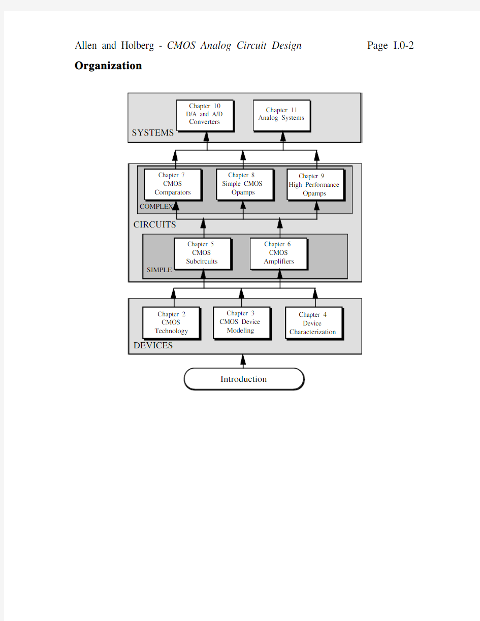
Organization
I.1 - INTRODUCTION
? Teach the analysis, modeling, simulation, and design of analog circuits implemented in CMOS technology.
? Emphasis will be on the design methodology and a hierarchical approach to the subject.
SPECIFIC OBJECTIVES
1. Present an overall, uniform viewpoint of CMOS analog circuit design.
2. Achieve an understanding of analog circuit design.
? Hand calculations using simple models
? Emphasis on insight
? Simulation to provide second-order design resolution
3. Present a hierarchical approach.
? Sub-blocks → Blocks → Circuits → Systems
4. Examples to illustrate the concepts.
I.2 ANALOG INTEGRATED CIRCUIT DESIGN ANALOG DESIGN TECHNIQUES VERSUS TIME FILTERS
DISCRETE VS. INTEGRATED ANALOG CIRCUIT DESIGN
Activity/Item Discrete Integrated Component Accuracy Well known Poor absolute accuracies Breadboarding?Yes No (kit parts) Fabrication Independent Very Dependent
Physical Implementation PC layout Layout, verification, and
extraction
Parasitics Not Important Must be included in the
design
Simulation Model parameters well
known Model parameters vary widely
Testing Generally complete
testing is possible Must be considered before the design
CAD Schematic capture,
simulation, PC board
layout Schematic capture, simulation, extraction, LVS, layout and routing
Components All possible Active devices,
capacitors, and resistors
THE ANALOG IC DESIGN PROCESS
COMPARISON OF ANALOG AND DIGITAL CIRCUITS Analog Circuits Digital Circuits
Signals are continuous in amplitude and can be continuous or discrete in time Signal are discontinuous in amplitude and time - binary signals have two amplitude states
Designed at the circuit level Designed at the systems level Components must have a continuum
of values
Component have fixed values Customized Standard
CAD tools are difficult to apply CAD tools have been extremely
successful
Requires precision modeling Timing models only Performance optimized Programmable by software Irregular block Regular blocks
Difficult to route automatically Easy to route automatically Dynamic range limited by power
supplies and noise (and linearity)
Dynamic range unlimited
I.3 TECHNOLOGY OVERVIEW
BANDWIDTHS OF SIGNALS USED IN SIGNAL PROCESSING APPLICATIONS
10
1
100
1k
10k
100k 1M 10M 100M 1G 10G
100G
Signal Frequency (Hz)
Signal frequency used in signal processing applications.
BANDWIDTHS THAT CAN BE PROCESSED BY PRESENT-DAY TECHNOLOGIES
Frequencies that can be processed by present-day technologies.
1011001k 10k
100k 1M 10M 100M 1G 10G 100G
Signal Frequency (Hz)
CLASSIFICATION OF SILICON TECHNOLOGY
BIPOLAR VS. MOS TRANSISTORS
CATEGORY BIPOLAR CMOS Turn-on Voltage0.5-0.6 V0.8-1 V Saturation Voltage0.2-0.3 V0.2-0.8 V
g m at 100μA 4 mS0.4 mS (W=10L) Analog Switch
Implementation
Offsets, asymmetric Good
Power Dissipation Moderate to high Low but can be large Speed Faster Fast
Compatible Capacitors Voltage dependent Good
AC Performance Dependence DC variables only DC variables and
geometry
Number of Terminals34 Noise (1/f)Good Poor Noise Thermal OK OK Offset Voltage< 1 mV5-10 mV
WHY CMOS???
CMOS is nearly ideal for mixed-signal designs:
? Dense digital logic
? High-performance analog
DIGITAL ANALOG
MIXED-SIGNAL IC
I.4 NOTATION
SYMBOLS FOR TRANSISTORS
Gate
Gate
Bulk n-channel, enhance-ment, V BS ≠ 0
n-channel, enhance-ment, bulk at most
negative supply
Gate
Gate
Bulk p-channel, enhance-ment, V BS ≠ 0
p-channel, enhance-ment, bulk at most positive supply
SYMBOLS FOR CIRCUIT ELEMENTS
-
A V -
G V
V 1v 1
V 1m V
I
Operational Amplifier/Amplifier/OTA
VCVS
VCCS
CCVS CCCS
Notation for signals
time