英文原文
12-Bit A/D Converter
CIRCUIT OPERATION
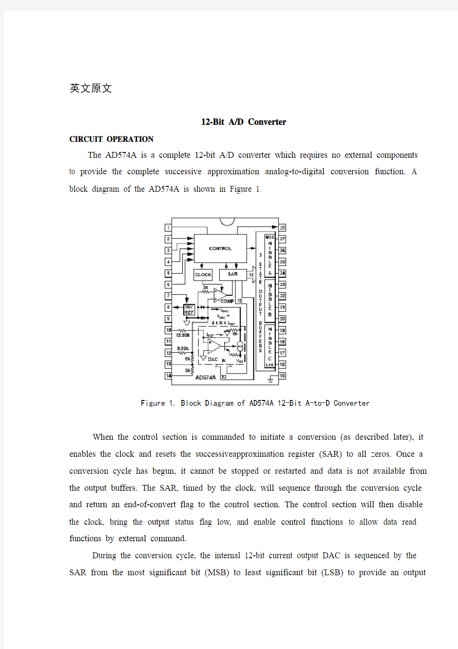
The AD574A is a complete 12-bit A/D converter which requires no external components to provide the complete successive approximation analog-to-digital conversion function. A block diagram of the AD574A is shown in Figure 1.
Figure 1. Block Diagram of AD574A 12-Bit A-to-D Converter
When the control section is commanded to initiate a conversion (as described later), it enables the clock and resets the successiveapproximation register (SAR) to all zeros. Once a conversion cycle has begun, it cannot be stopped or restarted and data is not available from the output buffers. The SAR, timed by the clock, will sequence through the conversion cycle and return an end-of-convert flag to the control section. The control section will then disable the clock, bring the output status flag low, and enable control functions to allow data read functions by external command.
During the conversion cycle, the internal 12-bit current output DAC is sequenced by the SAR from the most significant bit (MSB) to least significant bit (LSB) to provide an output
current which accurately balances the input signal current through the 5kΩ(or10kΩ) input resistor. The comparator determines whether the addition of each successively-weighted bit current causes the DAC current sum to be greater or less than the input current; if the sum is less, the bit is left on; if more, the bit is turned off. After testing all the bits, the SAR contains a 12-bit binary code which accurately represents the input signal to within 1/2 LSB.
The temperature-compensated buried Zener reference provides the primary voltage reference to the DAC and guarantees excellent stability with both time and temperature. The reference is trimmed to 10.00 volts 0.2%; it can s upply up to 1.5 mA to an external load in addition to the requirements of the reference input resistor (0.5 mA) and bipolar offset resistor (1 mA) when the AD574A is powered from 15 V supplies. If the AD574A is used with 12 V supplies, or if external cur rent must be supplied over the full temperature range, an external buffer amplifier is recommended. Any external load on the AD574A reference must remain constant during conversion. The thin-film application resistors are trimmed to match the full-scale output current of the DAC. There are two 5 k i nput scaling resistors to allow either a 10 volt or 20 volt span. The 10 k b ipolar offset resistor is grounded for unipolar operation and connected to the 10 volt reference for bipolar operation.
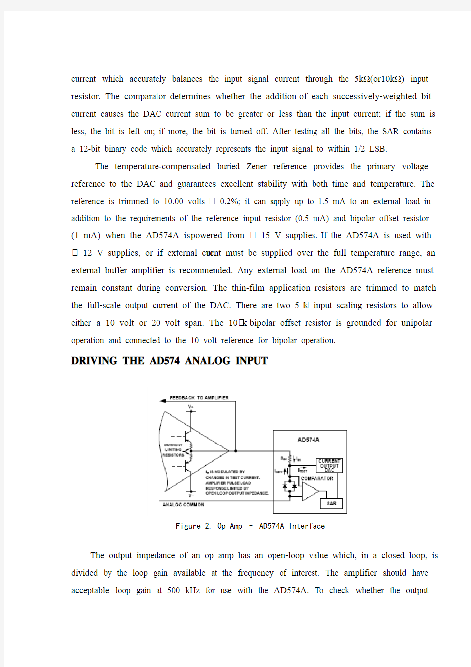
DRIVING THE AD574 ANALOG INPUT
Figure 2. Op Amp – AD574A Interface
The output impedance of an op amp has an open-loop value which, in a closed loop, is divided by the loop gain available at the frequency of interest. The amplifier should have acceptable loop gain at 500 kHz for use with the AD574A. To check whether the output
properties of a signal source are suitable, monitor the AD574’s input with an oscilloscope while a conversion is in progress. Each of the 12 disturbances should subside in sorless.
For applications involving the use of a sample-and-hold amplifier, the AD585 is recommended. The AD711 or AD544 op amps are recommended for dc applications. SAMPLE-AND-HOLD AMPLIFIERS
Although the conversion time of the AD574A is a maximum of 35 s, to achieve accurate 12-bit conversions of frequencies greater than a few Hz requires the use of a sample-and-hold amplifier (SHA). If the voltage of the analog input signal driving the AD574A changes by more than 1/2 LSB over the time interval needed to make a conversion, then the input requires a SHA.
The AD585 is a high linearity SHA capable of directly driving the analog input of the AD574A. The AD585’s fast acquisition time, low aperture and low aperture jitter are ideally suited for high-speed data acquisition systems. Consider the AD574A converter with a 35 s conversion time and an input signal of 10 V p-p: the maximum frequency which may be applied to achieve rated accuracy is 1.5 Hz. However, with the addition of an AD585, as shown in Figure 3, the maximum frequency increases to 26 kHz.
The AD585’s low output impedance, fast-loop response, and low droop maintain 12-bits of accuracy under the changing load conditions that occur during a conversion, making it suitable for use in high accuracy conversion systems. Many other SHAs cannot achieve 12-bits of accuracy and can thus compromise a system. The AD585 is recommended for AD574A applications requiring a sample and hold.
Figure 3. AD574A with AD585 Sample and Hold
SUPPLY DECOUPLING AND LAYOUT
CONSIDERATIONS
It is critically important that the AD574A power supplies be filtered, well regulated, and free from high frequency noise. Use of noisy supplies will cause unstable output codes. Switching power supplies are not recommended for circuits attempting to achieve 12-bit accuracy unless great care is used in filtering any switching spikes present in the output. Remember that a few millivolts of noise represents several counts of error in a 12-bit ADC.
Circuit layout should attempt to locate the AD574A, associated analog input circuitry, and interconnections as far as possible from logic circuitry. For this reason, the use of wire-wrap circuit construction is not recommended. Careful printed circuit construction is preferred.
UNIPOLAR RANGE CONNECTIONS FOR THE AD574A
The AD574A contains all the active components required to perform a complete 12-bit A/D conversion. Thus, for most situations, all that is necessary is connection of the power supplies (+5 V, +12 V/+15 V and –12 V/–15 V), the analog input, and the conversion initiation command, as discussed on the next page. Analog input connections and calibration are easily accomplished; the unipolar operating mode is shown in Figure 4.
Figure 4. Unipolar Input Connections
All of the thin-film application resistors of the AD574A are trimmed for absolute calibration. Therefore, in many applications, no calibration trimming will be required. The absolute accuracy for each grade is given in the specification tables. For example, if no trims are used, the AD574AK guarantees 1 LSB max zero offset error and 0.25% (10 LSB) max full-scale error. (Typical full-scale error is 2 LSB.) If the offset trim is not required, Pin 12 can be connected directly to Pin 9; the two resistors and trimmer for Pin 12 are then not needed. If the full-scale trim is not needed, a 50 1% metal film resistor should be connected between Pin 8 and Pin 10.
The analog input is connected between Pin 13 and Pin 9 for a 0 V to +10 V input range, between 14 and Pin 9 for a 0 V to +20 V input range. The AD574A easily accommodates an input signal beyond the supplies. For the 10 volt span input, the LSB has a nominal value of 2.44 mV; for the 20 volt span, 4.88 mV.
If a 10.24 V range is desired (nominal 2.5 mV/bit), the gain trimmer (R2) should be replaced by a 50Ωesistor, and a 200Ωt rimmer inserted in series with the analog input to Pin 13 for a full-scale range of 20.48 V (5 mV/bit), use a 500 t rimmer into Pin 14. The gain trim described below is now done with these trimmers. The nominal input impedance into Pin 13 is 5kΩ, and 10kΩi nto Pin 14.
UNIPOLAR CALIBRATION
The AD574A is intended to have a nominal 1/2 LSB offset so that the exact analog input for a given code will be in the middle of that code (halfway between the transitions to the codes above and below it). Thus, the first transition (from 0000 0000 0000 to 0000 0000 0001) will occur for an input level of +1/2 LSB (1.22 mV for 10 V range).
If Pin 12 is connected to Pin 9, the unit will behave in this manner, within specifications. If the offset trim (R1) is used, it should be trimmed as above, although a different offset can be set for a particular system requirement. This circuit will give approximately 15 mV of offset trim range.
The full-scale trim is done by applying a signal 1/2 LSB below the nominal full scale (9.9963 for a 10 V range). Trim R2 to give the last transition (1111 1111 1110 to 1111 1111 1111).
BIPOLAR OPERATION
The connections for bipolar ranges are shown in Figure 5. Again, as for the unipolar ranges, if the offset and gain specifications are sufficient, one or both of the trimmers shown can be replaced by a 50 1% fixed resistor. Bipolar calibration is similar to unipolar calibration.
Figure 5. Bipolar Input Connections
CONTROL LOGIC
The AD574A contains on-chip logic to provide conversion initiation and data read
operations from signals commonly available in microprocessor systems. Figure 6 shows the internal logic circuitry of the AD574A.
The control signals CE, CS, and R/C control the operation of the converter. The state of R/C when CE and CS are both asserted determines whether a data read (R/C = 1) or a convert (R/C = 0) is in progress. The register control inputs AO and 12/8 control conversion length and data format. The AO line is usually tied to the least significant bit of the address bus. If a conversion is started with AO low, a full 12-bit conversion cycleis initiated. If AO is high during a convert start, a shorter 8-bit conversion cycle results. During data read operations, AO determines whether the three-state buffers containing the 8 MSBs of the conversion result (AO = 0) or the 4 LSBs (AO = 1) are enabled. The 12/8 pin determines whether the output data is to be organized as two 8-bit words (12/8 tied to DIGITAL COMMON) or a single 12-bit word (12/8 tied to VLOGIC). The 12/8 pin is not TTL-compatible and must be hard-wired to either VLOGIC or DIGITAL COMMON. In the 8-bit mode, the byte addressed when AO is high contains the 4 LSBs from the conversion followed by four trailing zeroes. This organization allows the data lines to be overlapped for direct interface to 8-bit buses without the need for external three-state buffers. It is not recommended that AO change state during a data read operation. Asymmetrical enable and disable times of the three-state buffers could cause internal bus contention resulting in potential damage to the AD574A.
Figure 6. AD574A Control Logic
An output signal, STS, indicates the status of the converter. STS goes high at the beginning of a conversion and returns low when the conversion cycle is complete.
TIMING
The AD574A is easily interfaced to a wide variety of microprocessors and other digital systems. The following discussion of the timing requirements of the AD574A control signals should provide the system designer with useful insight into the operation of the device.
Figure 7 shows a complete timing diagram for the AD574A convert start operation. R/C should be low before both CE and CS are asserted; if R/C is high, a read operation will momentarily occur, possibly resulting in system bus contention. Either CE or CS may be used to initiate a conversion; however, use of CE is recommended since it includes one less propagation delay than CS and is the faster input. In Figure 7, CE is used to initiate the conversion.
Figure 7
Once a conversion is started and the STS line goes high, convert start commands will be ignored until the conversion cycle is complete. The output data buffers cannot be enabled during conversion.
Figure 8 shows the timing for data read operations. During data read operations, access time is measured from the point where CE and R/C both are high (assuming CS is already low). If CS is used to enable the device, access time is extended by 100 ns.
Figure 8. Read Cycle Timing
In the 8-bit bus interface mode (12/8 input wired to DIGITAL COMMON), the address bit, AO, must be stable at least 150 ns prior to CE going high and must remain stable during the entire read cycle. If AO is allowed to change, damage to the AD574A output buffers may result.
“STAND-ALONE” OPERATION
The AD574A can be used in a ―stand-alone‖ mode, which is useful in systems with dedicated input ports available and thus not requiring full bus interface capability. In this mode, CE and 12/8 are wired high, CS and AO are wired low, and conversion is controlled by R/C. The three-state buffers are enabled when R/C is high and a conversion starts when R/C goes low. This allows two possible control signals—a high pulse or a low pulse. Operation with a low pulse is shown in Figure 11. In this case, the outputs are forced into the high impedance state in response to the falling edge of R/C and return to valid logic levels after the conversion cycle is completed. The STS line goes high 600 ns after R/C goes low and returns low 300 ns after data is valid.
Figure 11. Low Pulse for R/C—Outputs Enabled After Conversion
If conversion is initiated by a high pulse as shown in Figure 12, the data lines are enabled during the time when R/C is high. The falling edge of R/C starts the next conversion, and the data lines return to three-state (and remain three-state) until the next high pulse of R/C.
Figure 12. High Pulse for R/C—Outputs Enabled While R/C High, Otherwise High-Z
Usually the low pulse for R/C stand-alone mode will be used. Figure 13 illustrates a typical stand-alone configuration for 8086 type processors. The addition of the 74F/S374 latches improves bus access/release times and helps minimize digital feedthrough to the analog portion of the converter.
INTERFACING THE AD574A TO MICROPROCESSORS
The control logic of the AD574A makes direct connection to most microprocessor system buses possible. While it is impossible to describe the details of the interface connections for every microprocessor type, several representative examples will be described here.
GENERAL A/D CONVERTER INTERFACE
CONSIDERATIONS
A typical A/D converter interface routine involves several operations. First, a write to the ADC address initiates a conversion.The processor must then wait for the conversion cycle to complete, since most ADCs take longer than one instruction cycle to complete a conversion. Valid data can, of course, only be read after the conversion is complete. The AD574A provides an output signal (STS) which indicates when a conversion is in progress. This signal can be polled by the processor by reading it through an external three-state buffer (or other
input port). The STS signal can also be used to generate an interrupt upon completion of conversion, if the system timing requirements are critical (bear in mind that the maximum conversion time of the AD574A is only 35 microseconds) and the processor has other tasks to perform during the ADC conversion cycle. Another possible time-out method is to assume that the ADC will take 35 microseconds to convert, and insert a sufficient number of ―do-nothing‖ instructions to ensure that 35 microseconds of processor time is consumed Once it is established that the conversion is finished, the data can be read. In the case of an ADC of 8-bit resolution (or less), a single data read operation is sufficient. In the case of converters with more data bits than are available on the bus, a choice of data formats is required, and multiple read operations are needed. The AD574A includes internal logic to permit direct interface to 8-bit or 16-bit data buses, selected by connection of the 12/8 input. In 16-bit bus applications (12/8 high) the data lines (DB11 through DB0) may be connected to either the 12 most significant or 12 least significant bits of the data bus. The remaining four bits should be masked in software. The interface to an 8-bit data bus (12/8 low) is done in a left-justified format. The even address (A0 low) contains the 8 MSBs (DB11 through DB4). The odd address (A0 high) contains the 4 LSBs (DB3 through DB0) in the upper half of the byte, followed by four trailing zeroes, thus eliminating bit masking instructions.
SPECIFIC PROCESSOR INTERFACE EXAMPLES
Z-80 System Interface
The AD574A may be interfaced to the Z-80 processor in an I/O or memory mapped configuration. Figure 15 illustrates an I/O or mapped configuration. The Z-80 uses address lines A0–A7 to decode the I/O port address.
An interesting feature of the Z-80 is that during I/O operations a single wait state is automatically inserted, allowing the AD574A to be used with Z-80 processors having clock speeds up to 4 MHz. For applications faster than 4 MHz use the wait state generator in Figure 16. In a memory mapped configuration the AD574A may be interfaced to Z-80 processors with clock speeds of up to 2.5 MHz.
附录E 中文翻译
12位-AD574A转换器
电路工作原理
AD574A是一个完善的12位A/D转换器,不需要外部组件提供完全的逐步逼近模拟数字转换功能。图1所示为AD574A的方块结构图。
图1 AD574A的方块结构图
当控制部分收到初始化转换命令(后边会叙述)时,会开启时钟并把连续逼近寄存器(SAR)全部置零。一旦转换周期开始,它就不能终止或重新开始,也不能从输出缓冲中读数。时钟控制SAR寄存器的时序,SAR会安排好转换周期的顺序并向控制部分返回一个“转换结束”(end-of-convert)标志。接着,控制部分停止时钟,把输出状态标志位置低,并允许控制函数,以便外部命令可以执行数据读取功能。
在转换周期期间, 内部12 位当前的产品DAC 由SAR 程序化从最高位(MSB) 对最低有效位(LSB)通过5 k(或10k) 输入电阻器提供准确地平衡输入信号。比较器确定位电流的连续增大是否造成了DAC当前总电流比输入电流增大或者减小; 如果总电流较小,此位被留下; 如果总电流较大,位被关闭。在测试完所有位以后, SAR包含了准确表示输入信号在+1/2 LSB之内的12位二进制编码。
温度补偿是外部提供给DAC基准电压并保证准确的转换的时间和温度的稳定性。基准在10.00 0.2%伏之间平衡,当AD574A使用15伏电源时,除了按要求向参考输入电阻提供0.5mA,向双极偏移电阻提供1mA电流外,它可以给外部负载提供提供高至1.5mA 的电流。如果AD574A使用12伏电源,或者外部电流必须在全部温度范围内提供,那么我们推荐使用一个外部的缓冲放大器。任何在AD574A参考手册上的外部负载都必须在转换过程中保持稳定。要调整薄膜应用电容以匹配DAC(数模转换器)的实比例输出电流。有两个5千欧的输入测量电阻允许10伏或20伏的区间。10千欧的双极偏移电容接地用于单极操作,或连接到10伏参考电压上用于双极性操作。
AD574模拟输入电压
图2 OP放大器与AD574连接
OP放大器的输出阻抗有一个开环值,在一个封闭回路中,这个值被回路增益(由增加的频率产生)等分。放大器应该至少拥有500kHz的回路增益才能和AD574A一起使用。要检查信号源的输出特性是否合适,就要在转换进行中使用示波镜监控AD574的输入端。每12个干扰应该在1秒以内衰减。
关于取样—保持器的应用,我们推荐AD585型号。我们推荐让AD711型号和AD544型号取样—保持器应在直流电下工作。
虽然AD574A的转换时间最高为35秒,但为了能够实现几个赫兹的频率的精确12位转换还是需要使用采样-保持放大器(SHA)的。如果一个驱动AD574A的模拟输入信号电压在转换所需的计时周期中变化超过LSB的一半,那么输入端就需要一个SHA。
AD585是一种高线性的采样-保持放大器(SHA),它能够直接驱动AD574A的模拟输
入端。AD585的快速采集时间、低孔径和低孔径抖动都很好地使用于高速数据采集系统。考虑到AD574A的转换时间为35秒,并且拥有10Vp-p的输入信号,这是能够实现1.5Hz 精确转换时所能用的最高频率。如图3所示,加上AD585后,最高频率增加到了26kHz。
AD585的低输出阻抗、快速连环反应和低损耗能够在变化的周期性负荷工况下维持12位准确性,使它适当用于高精确度转换。许多其他SHAs达不到12位转换的准确性,并且可能因而减弱系统。AD585被推荐应用于AD574A的采样与保持。
图3 带采样保持器AD585的AD574A
AD574A 电源的滤波、良好地校准和远离高频噪声是异常重要的.。噪声补偿的使用会造成不稳定的输出信号。除非特别要求滤掉输出端的电火花,交换式电源电路建议达到12比特的精确度。注意:一点点毫伏的噪声就代表着12比特ADC(电源)的巨大误差。
电路布局应该尝试定位AD574A,与之相连的相似物输入电路,并使其从逻辑电路上尽可能连接起来.因为这个原因,不推荐使用线路电路结构.应该选择好的印刷的电路体系.
AD574A处理单极性信号
AD574A包括了所有进行完全12位AD转换所需的活动组件。这样,在大多数情况下,所需的只是电源连接(+5 V, +12 V/+15 V 和–12 V/–15 V)、模拟输入以及转换
初始化命令,下页会讨论到。模拟输入连接和校准都很容易完成。单极操作模式如图4所示。
图4
AD574A所有的薄膜应用程序电阻是通过绝对刻度来衡量的。因此在许多应用程序中,并不需要刻度平衡。规格表给出了每个等级的绝对精度。例如,如果没有应用区标,AD574AK保证1LSB最大零偏移误差和0.25% (10LSB)最大满额误差。(通常满额误差是2 LSB)。如果不允许使用这个弯管平衡的话,pin 12 可以直接同pin 9连接;pin 12 的这两个电阻器和这个微调电容器就不需要了。如果不允许使用完整的平衡,应该在pin 8和pin 10之间连接一个xxxx金属薄膜微调电容器。
此器件在输入电压0到10伏连接时须接脚9和脚13,当输入电压在0到20伏之间时,应从脚14和脚9引入。AD574A提供输入信号补偿,输入电压在10伏以内时理论值是2.44mV,在输入电压在20伏以内时理论值是2.44mV
如果电压达到10.24(也就是2.5mv/bit) , 增益可调电阻就必须调整为50 .一个200Ω可变电阻串连到模拟输入引脚13其满刻度值为20.48V(5 mV/bit),用500Ω的可变电阻串连到模拟输入引脚14.下述增益的调整用这些可变电阻完成.引脚13的名义输入阻抗为5 k Ω, 而插脚14的名义输入阻抗为10kΩ。
单极性输入
AD574A拥有一个名义上是LSB一半的偏移量,以便对一个给定编码的准确模拟输
入可以正好处于这个编码的中央(在其前后各有一半的编码转换)。这样,第一个转换(从0000 0000 0000到0000 0000 0001)会在输入电平为+1/2LSB(对于10V的范围来说是1.22mV)时发生。
如果第12脚连在第9脚上,那么单元将在规格之内按此方式工作。如果使用了偏移调整(R1),虽然可以针对特定的系统要求设置不同的偏移量,但也应该按上述方法调整。这个电路会给出大约15mV的偏移调整范围。
满量程调整适用于一个信号在满量程下产生1/2 LSB线性误差,也就是对于10V范围来说是9.9963。调整R2来实现最后一个转换(1111 1111 1110到1111 1111 1111)
双极性输入
双极的联系范围如图5。还有,就单极的范围,如果输出量与增加量的数据充足的话,一个电容器或者两个都可以拿一个50±1%的固定电阻来代替。单极标准与双极标准是相似的。
图5
逻辑控制
AD574A包含了芯片上逻辑,可以通过微处理器中通常存在的信号中提供开始转换和读取转换结果操作‖ 如图6是AD574A的内部逻辑电路。
控制信号CE 、CS, 和R/C 控制交换器的操作。R/C 的状态由CE 和CS 两个信号
的加入来确定进行数据读取(R/C = 1) 或数据转换(R/C = 0) 。记数器控制输入AO ,12/8 控制转换长度和数据格式。AO 线通常被连结到地址总线的最低有效位。如果AO置低(电位)开始, 按12 位A/D进行转换。当12/8=1时,12位数据线一次读出,主要用于16位微机系统;12/8=0时,可与8位机接口。此引脚输入为高电平时,12位数据并行输出;当此引脚为低电平时,与引脚A0配合,把12位数据分两次输出。12/8的引脚接DIGITAL COMMON输出8位数据12/8引脚接VLOGIC输出12位数据。12/8的引脚不与TTL兼容的,必须和vlogic或者digital连接,在8位模式下,当Ao置高的时候,低4位加上尾随4个0有效。在不需要内部3态缓冲器的情况下,该结构允许直接接口的8位数据流重叠。在读取转换数据操作时不建议ao改变。三态缓冲器不对称的允许与阻止时间可能造成内部总线冲突,对AD574A造成潜在危害
.
STS这个输出信号表明了转换器的状况。STS值在转换开始时升高,在转换过程完成后降低回原样。
AD574A 容易联接于多种微处理器和其他数字化系统。下列AD574A控制信号的计时要求的讨论应该为系统设计者提供有用的对设备的操作了解。
图7
图7显示的是完整的AD574A运作时间矢量图表.坐标轴R/C在CE和CS被捕获之前都应较低;如果R/C显示较高,操作提示会立即发生,并可能引发系统争用.无论CE还是CS都能被用来转换.但是,我们推荐使用CE,因为它比CS有更少的系统延迟,并且能被较快地输入.在图表7,CE被用来转换.
一旦转换开始STS置成高位,直到转换循环完成,转换开始命令将被忽略。直到转换周期是完全的。在转换期间,输出数据缓冲无效。
图8给出了数据读取操作时间状况,在数据读取过程中, 当CE和R/C都处于高电平(假定CS已经处于低电平)的时候,开始测量访问时间. 如果这时CS能够使得设备工作, 访问时间可延长100纳秒.
图8
在8位的总线接线模式中(和数字公用区连线的12/8 输出),地址位AO,必须在CE 升高的150毫秒之前和整个读取循环中保持稳定。如果允许AO变化,将会导致对AD574A 输出缓存区的损坏。
AD5474A单机操作
AD5474A可以“独立”模式使用,它是系统里很好用的、可用的和专用的端口,以这种方式不需要用总线连接。按这方式,CE和12/8置成高位,CS和AO置成低位,而转化由RC控制。当RC置成高位时,三态缓冲器启动,当RC置成低位时开始转换。其允许两种控制信号一种高电位脉冲,低高电位脉冲。由如图11所示的低脉冲操作。在这种情况下R/C下降沿的输出响应被强制为高阻状态,在一个转换周期结束后置回有效逻辑。STS 线在R/C变为低电平600ns后变为高电平,当数据有效300ns后恢复低电平。
图9
如果转换是由如图12所示的高电平脉冲所初始化的,那么在R/C为高电平时,数据链是被允许的。R/C的下降沿启动下一个转换,并且数据链返回到三态(并一直保持三态),知道下一个R/C高电平脉冲出现。
图10
通常应用R/C单机模式下的低脉冲。图13阐明了典型的8086型处理机的单机构造。额外的74F/S374 插销提高了总线的访问/放行次数并协助简化转炉数-模部分的连接
线。
图11
AD574与单片机接口
AD574A的控制逻辑使得绝大多数情况下和微处理器系统总线直接连线变成可能。然而它不可能描述出每一种微处理器类型的接口连接的所有细节,下面将举几个具有代表性的例子。
典型的数模转换器接口程序序列涉及以下几步:首先, 在初始化会话的时候,地址被写进数模转换。处理器必须等待会话周期的结束,因为多数数模转换器需要一个以上的指令周期来完成会话操作。当然,有效数据只有在会话结束后才能被读取。AD574A 提供信号端输出(STS) ,它能指示会话过程。这个信号可以由处理器通过读取外部三态缓冲(或其它输入端口)获得。如果系统的计时要求非常严格(请记住AD574A的最大转换时间只有35毫秒)并且处理器在ADC转换周期中有其它任务要做的话,这个STS信号同样可以用于产生一个中断信号传递给转换过程。另一种可行的延时方法是,先假设模数转换器会消耗35微秒来进行转换,然后插入足够多的空指令来保证处理器消耗掉35微秒的时间。
一旦建立,即完成转换,可以读取数据.在8位(或数位更少)ADC的情况下,单次读数运行即已足够.在转换器数位多于总线可使用数位的情况下,须选择数据格式,需进行多重读数运行.AD574A含有内部逻辑(器),允许通过选择连接12/8输入而直接到8位或多或16位数据总线界面上。在采用16位数据总线时,(12/8 高)数据总线(DB11 通过 DB0)既可以连接到数据总线的12位有效位或12位无效位。剩余4位应用软件将其掩蔽.到8位数据总线的界面是采用左优格式来实现的。在数位的上半部偶数地址(A0 低)包含 8 MSBs (DB11 通过 DB4).。奇数地址(A0 高)包含 4 LSBs (DB3 through DB0),后面跟有4个零,从而消除数位掩蔽指令.
Photoshop中英文对照 1、File 文件 New 新建 Open 打开 Open As 打开为 Open Recent 最近打开文件 Close 关闭 Save 存储 Save As 存储为 Save for Web 存储为Web所用格式Revert 恢复 Place 置入 Import 输入 PDF Image PDF图象导入Annotations 注释 Export 输出 Manage Workflow 管理工作流程Check In 登记 Undo Check Out 还原注销 Upload To Server 上载到服务器Add To Workflow 添加到工作流程 Open From Workflow 从工作流程打开 Automate 自动 Batch 批处理 Create Droplet 创建快捷批处理 Conditional Mode Change 条件模式更改 Contact Sheet 联系表 Fix Image 限制图像 Multi Page PDF to PSD 多页面PDF文件到PSD文件 Picture package 图片包 Web Photo Gallery Web照片画廊File Info 文件简介 Print Options 打印选项 Page Setup 页面设置 Print 打印 Jump to 跳转到 Exit 退出 2、Edit 编辑 Undo 还原 Step Forward 向前 Step Backward 返回 Fade 消退 Cut 剪切 Copy 拷贝 Copy Merged 合并拷贝 Paste 粘贴 Paste Into 粘贴入 Clear 清除 Fill 填充 Stroke 描边 Free Transform 自由变形Transform 变换 Again 再次 Scale 缩放 Rotate 旋转 Skew 斜切 Distort 扭曲 Perspective 透视 Rotate 180°旋转180度 Rotate 90°CW 顺时针旋转90度Rotate 90°CCW 逆时针旋转90度
微软Visual Studio 1微软Visual Studio Visual Studio 是微软公司推出的开发环境,Visual Studio可以用来创建Windows平台下的Windows应用程序和网络应用程序,也可以用来创建网络服务、智能设备应用程序和Office 插件。Visual Studio是一个来自微软的集成开发环境IDE,它可以用来开发由微软视窗,视窗手机,Windows CE、.NET框架、.NET精简框架和微软的Silverlight支持的控制台和图形用户界面的应用程序以及Windows窗体应用程序,网站,Web应用程序和网络服务中的本地代码连同托管代码。 Visual Studio包含一个由智能感知和代码重构支持的代码编辑器。集成的调试工作既作为一个源代码级调试器又可以作为一台机器级调试器。其他内置工具包括一个窗体设计的GUI应用程序,网页设计师,类设计师,数据库架构设计师。它有几乎各个层面的插件增强功能,包括增加对支持源代码控制系统(如Subversion和Visual SourceSafe)并添加新的工具集设计和可视化编辑器,如特定于域的语言或用于其他方面的软件开发生命周期的工具(例如Team Foundation Server的客户端:团队资源管理器)。 Visual Studio支持不同的编程语言的服务方式的语言,它允许代码编辑器和调试器(在不同程度上)支持几乎所有的编程语言,提供了一个语言特定服务的存在。内置的语言中包括C/C + +中(通过Visual C++),https://www.doczj.com/doc/2d15795496.html,(通过Visual https://www.doczj.com/doc/2d15795496.html,),C#中(通过Visual C#)和F#(作为Visual Studio 2010),为支持其他语言,如M,Python,和Ruby等,可通过安装单独的语言服务。它也支持的 XML/XSLT,HTML/XHTML ,JavaScript和CSS.为特定用户提供服务的Visual Studio也是存在的:微软Visual Basic,Visual J#、Visual C#和Visual C++。 微软提供了“直通车”的Visual Studio 2010组件的Visual Basic和Visual C#和Visual C + +,和Visual Web Developer版本,不需任何费用。Visual Studio 2010、2008年和2005专业版,以及Visual Studio 2005的特定语言版本(Visual Basic、C++、C#、J#),通过微软的下载DreamSpark计划,对学生免费。 2架构 Visual Studio不支持任何编程语言,解决方案或工具本质。相反,它允许插入各种功能。特定的功能是作为一个VS压缩包的代码。安装时,这个功能可以从服务器得到。IDE提供三项服务:SVsSolution,它提供了能够列举的项目和解决方案; SVsUIShell,它提供了窗口和用户界面功能(包括标签,工具栏和工具窗口)和SVsShell,它处理VS压缩包的注册。此外,IDE还可以负责协调和服务之间实现通信。所有的编辑器,设计器,项目类型和其他工具都是VS压缩包存在。Visual Studio 使用COM访问VSPackage。在Visual Studio SDK中还包括了管理软件包框架(MPF),这是一套管理的允许在写的CLI兼容的语言的任何围绕COM的接口。然而,MPF并不提供所有的Visual Studio COM 功能。
商务英语口语900句中英文对照中文翻译 Unit 1希望与要求 Part 1 . 1. We'd like to express our desire to establish business relationship with you on the basis of quality, mutually benefit and exchange of needed goods . 我们希望在保证质量、互惠互利以及交易彼此需要的货物的基础上和你们建立业务关系。 2 .In order to extend our export business to your country we wish to enter direct business relations with you. 为了扩大我们在贵国的出口业务,我们希望和你们建立直接贸易关系。 3. Our hope is to establish mutually beneficial trading relations between us . 希望在我们之间能够建立互惠互利的贸易关系。 4. We looking forward to further extensions of pleasant business relations. 我们期待进一步保持愉快的业务关系。 5. It’s our hope to continue with considerable business dealing with you. 我们的希望是和你们保持可观的生意往来。 6. We looking forward to receiving your quotation very soon. 我们期待尽快收到你们的报价单。 7.I hope you see from the reduction that we are really doing our utmost. 我希望你能够看到我们事实上已经作出了最大程度的让价。 8.We hope to discuss business with you at your earliest convenience. 我们希望在你方便的时候和你洽谈业务。
毕业设计(论文)外文参考文献及译文 英文题目Component-based Safety Computer of Railway Signal Interlocking System 中文题目模块化安全铁路信号计算机联锁系统 学院自动化与电气工程学院 专业自动控制 姓名葛彦宁 学号 200808746 指导教师贺清 2012年5月30日
Component-based Safety Computer of Railway Signal Interlocking System 1 Introduction Signal Interlocking System is the critical equipment which can guarantee traffic safety and enhance operational efficiency in railway transportation. For a long time, the core control computer adopts in interlocking system is the special customized high-grade safety computer, for example, the SIMIS of Siemens, the EI32 of Nippon Signal, and so on. Along with the rapid development of electronic technology, the customized safety computer is facing severe challenges, for instance, the high development costs, poor usability, weak expansibility and slow technology update. To overcome the flaws of the high-grade special customized computer, the U.S. Department of Defense has put forward the concept:we should adopt commercial standards to replace military norms and standards for meeting consumers’demand [1]. In the meantime, there are several explorations and practices about adopting open system architecture in avionics. The United Stated and Europe have do much research about utilizing cost-effective fault-tolerant computer to replace the dedicated computer in aerospace and other safety-critical fields. In recent years, it is gradually becoming a new trend that the utilization of standardized components in aerospace, industry, transportation and other safety-critical fields. 2 Railways signal interlocking system 2.1 Functions of signal interlocking system The basic function of signal interlocking system is to protect train safety by controlling signal equipments, such as switch points, signals and track units in a station, and it handles routes via a certain interlocking regulation. Since the birth of the railway transportation, signal interlocking system has gone through manual signal, mechanical signal, relay-based interlocking, and the modern computer-based Interlocking System. 2.2 Architecture of signal interlocking system Generally, the Interlocking System has a hierarchical structure. According to the function of equipments, the system can be divided to the function of equipments; the system
A Wavelet Based Approach for Fast Detection of Internal Fault in Power Transformers The power transformer is one of the most expensive elements of power system and its protection is an essential part of the overall system protection strategy. The differential protection provides the best protection for power transformer. Its operation principle is based on this point that the differential current during an internal fault is higher than normal condition. But, a large transient current (inrush current) can cause mal-operation of differential relays. Then, studies for the improvement of the transformer protection have focused on discrimination between internal short circuit faults and inrush currents in transformers. The magnetizing inrush current has a large second order harmonic component in comparison to internal faults. Therefore , some transformer protection systems are designed to halt operating during the inrush current by sensing this large second order harmonic. The second harmonic component in the magnetizing inrush currents tend to be relatively small in modern large power transformers because of improvements in the power transformer core materials. Also , it has been seen that the fault current can contain higher second order harmonics than the inrush current due to nonlinear fault resistance, CT saturation .the distributed capacitance in the transmission line, which transformer is connected to, or due to the use of extra high voltage underground cables. Various methods have been suggested for overcoming this protection system mal-operation. This paper presents a wavelet based method for discrimination among inrush current, internal short circuit ,external short circuit and energizing and it is not affected by CT saturation and it is able to detect internal faults while transformer energization. Unlike Artificial Neural Network and Fuzzy logic based algorithms. This approach is not system dependent. The operating time of the scheme is less than 10ms. The Daubechies mother wavelet is used with a sample rate of 5 kHz. Then , the differential currents of the three phases are decomposed into two details and only the second level will be considered by using db5 mother wavelet. Discrete Wavelet Transform The wavelet transform is a powerful tool to extract information from the non-stationary signals simultaneously in both time and frequency domains. The ability of the wavelet transform to focus on short time intervals for high-frequency components and long intervals for low-frequency components improves the analysis
中英文对照翻译 (文档含英文原文和中文翻译) Policies for Development of Iron and Steel Industry The iron and steel industry is an important basic industry of the national economy, a supporting industry for realizing the industrialization and an intensive industry in technologies, capital, resources and energy, and its development requires a comprehensive balancing of all kinds of external conditions. China is a big developing country with a comparatively big demand of iron and steel in the economic development for a long time to go. China's production capacity of iron and steel has ranked the first place in the world for many years. However, there is a large gap in terms of the technological level and material consumption of the iron and steel industry compared with the international advanced level, so the focus of development for the future shall be put on technical upgrading and structural adjustment. In order to enhance the whole technical level of the iron and steel industry, promote the structural adjustment, improve the industrial layout, develop a recycling economy, lower the consumption of materials and energy, pay attention to the environmental protection, raise the comprehensive competitive capacity of enterprises, realize the industrial upgrading, and develop the iron and steel industry into an industry with
文献翻译 原文 Combining JSP and Servlets The technology of JSP and Servlet is the most important technology which use Java technology to exploit request of server, and it is also the standard which exploit business application .Java developers prefer to use it for a variety of reasons, one of which is already familiar with the Java language for the development of this technology are easy to learn Java to the other is "a preparation, run everywhere" to bring the concept of Web applications, To achieve a "one-prepared everywhere realized." And more importantly, if followed some of the principles of good design, it can be said of separating and content to create high-quality, reusable, easy to maintain and modify the application. For example, if the document in HTML embedded Java code too much (script), will lead the developed application is extremely complex, difficult to read, it is not easy reuse, but also for future maintenance and modification will also cause difficulties. In fact, CSDN the JSP / Servlet forum, can often see some questions, the code is very long, can logic is not very clear, a large number of HTML and Java code mixed together. This is the random development of the defects. Early dynamic pages mainly CGI (Common Gateway Interface, public Gateway Interface) technology, you can use different languages of the CGI programs, such as VB, C / C + + or Delphi, and so on. Though the technology of CGI is developed and powerful, because of difficulties in programming, and low efficiency, modify complex shortcomings, it is gradually being replaced by the trend. Of all the new technology, JSP / Servlet with more efficient and easy to program, more powerful, more secure and has a good portability, they have been many people believe that the future is the most dynamic site of the future development of technology. Similar to CGI, Servlet support request / response model. When a customer submit a request to the server, the server presented the request Servlet, Servlet responsible for handling requests and generate a response, and then gave the server, and then from the server sent to
PLC论文中英文对照资料外文翻译文献 外文资料: PLC technique discussion and future development Along with the development of the ages, the technique that is nowadays is also gradually perfect, the competition plays more more strong; the operation that list depends the artificial has already can't satisfied with the current manufacturing industry foreground, also can't guarantee the request of the higher quantity and high new the image of the technique business enterprise. The people see in produce practice, automate brought the tremendous convenience and the product quantities for people up of assurance, also eased the personnel's labor strength, reduce the establishment on the personnel. The target control of the hard realization in many complicated production lines, whole and excellent turn, the best decision etc., well-trained operation work, technical personnel or expert, governor but can judge and operate easily, can acquire the satisfied result. The research target of the artificial intelligence makes use of the calculator exactly to carry out, imitate these intelligences behavior, moderating the work through person's brain and calculators, with the mode that person's machine combine, for resolve the very complicated problem to look for the best path We come in sight of the control that links after the electric appliances in various situation, that is already the that time generation past, now of after use in the mold a perhaps simple equipments of grass-roots control that the electric appliances can do for the low level only;And the PLC emergence also became the epoch-making topic, adding the vivid software control through a very and stable hardware, making the automation head for the new high tide. The PLC biggest characteristics lie in: The electrical engineering teacher already no longer electric hardware up too many calculationses of cost, as long as order the importation that the button switch or the importation of the sensors order to link the PLC up can solve problem, pass to output to order the conjunction contact machine or control the start equipments of the
VOLUME 30 ISSUE 2 October 2008 Journal of Achievements in Materials and Manufacturing Engineering Copyright by International OCSCO World Press. All rights reserved.2008 151 Research paper 2008年十月期2卷30 材料与制造工程成果期刊 版权所有:国际OCSCO 世界出版社。一切权利保有。2008 ??151研究论文 1. Introduction Friction stir welding (FSW) is a new solid-state welding method developed by The Welding Institute (TWI) in 1991 [1]. The weld is formed by the excessive deformation of the material at temperatures below its melting point, thus the method is a solid state joining technique. There is no melting of the material, so FSW has several advantages over the commonly used fusion welding techniques [2-10]. 1.导言摩擦搅拌焊接(FSW)是焊接学?会于1991年研发的一种新型固态焊接方法。这种焊接?是由材料在低于其熔点的温度上过量变形形成,因此此技术是一种固态连接技术。材料不熔化,所以FSW 相比常用的熔化焊接技术有若干优势。例如,在焊接区无多孔性或破裂,工件(尤其薄板上)没有严重扭曲,并且在连接过程中不需要填料、保护气及昂贵的焊接准备there is no significant distortion of the workpieces (particularly in thin plates), and there is no need for filler materials, shielding gases and costly weld preparation during this joining process. FSW被认为是对若干材料例如铝合金、镁合金、黄铜、钛合金及钢最显著且最有潜在用途的焊接技术FSW is considered to be the most remarkable and potentially useful welding technique for several materials, such as Al-alloys, Mg-alloys, brasses, Ti-alloys, and steels [1-16]. 然而,在FSW过程中,用不合适的焊接参数能引起连接处失效,并且使FSW连接处的力学性能恶化。However, during FSW process using inappropriate welding parameters can cause defects in the joint and deteriorate the mechanical properties of the FSW joints [2, 3]. 此技术起初就主要是为低熔点材料如铝合金、镁合金及铜合金而广泛研究的。The technique has initially been widely investigated for mostly low melting materials, such as Al, Mg and Cu alloys. 此技术已被证明是很有用的,尤其在连接用于航空航天用途的如高合金2XXX及7XXX系列铝合金等难熔高强度的铝合金。It has proven to be very useful, particularly in the joining of the difficult-to-fusion join high strength Al-alloys used in aerospace applications, such as highly alloyed 2XXX and 7XXX series aluminium alloys. 做出Al-5086 H32型板摩擦搅拌对焊的高强度、抗疲劳及断裂的力学性能?。The difficulty of making high-strength, fatigue and fracture resistant Mechanical properties of friction stir butt-welded Al-5086 H32 plate G. .am a,*, S. Gü.lüer b, A. .akan c, H.T. Serinda. a a Mustafa Kemal University, Faculty of Engineering and Architecture, 31040 Antakya, Turkey a 土耳其安塔卡亚31040,Mustafa Kemal大学建筑工程系 b General Directorate of Highways of Turkey, Ankara, Turkey b 土耳其安卡拉土耳其高速公路总理事会? c Abant Izzet Baysal University, Faculty of Engineering an d Architecture, 14280 Bolu, Turkey c 土耳其Bolu 14280 Abant Izzet Baysal 大学建筑工程系 * Corresponding author: E-mail address: gurelcam@https://www.doczj.com/doc/2d15795496.html, *相关作者电子邮箱地址:gurelcam@https://www.doczj.com/doc/2d15795496.html, Received 30.06.2008; published in revised form 01.10.2008
中英文对照资料外文翻译文献 平设计任何时期平面设计可以参照一些艺术和专业学科侧重于视觉传达和介绍。采用多种方式相结合,创造和符号,图像和语句创建一个代表性的想法和信息。平面设计师可以使用印刷,视觉艺术和排版技术产生的最终结果。平面设计常常提到的进程,其中沟通是创造和产品设计。共同使用的平面设计包括杂志,广告,产品包装和网页设计。例如,可能包括产品包装的标志或其他艺术作品,举办文字和纯粹的设计元素,如形状和颜色统一件。组成的一个最重要的特点,尤其是平面设计在使用前现有材料或不同的元素。平面设计涵盖了人类历史上诸多领域,在此漫长的历史和在相对最近爆炸视觉传达中的第20和21世纪,人们有时是模糊的区别和重叠的广告艺术,平面设计和美术。毕竟,他们有着许多相同的内容,理论,原则,做法和语言,有时同样的客人或客户。广告艺术的最终目标是出售的商品和服务。在平面设计,“其实质是使以信息,形成以思想,言论和感觉的经验”。
在唐朝(618-906 )之间的第4和第7世纪的木块被切断打印纺织品和后重现佛典。阿藏印在868是已知最早的印刷书籍。在19世纪后期欧洲,尤其是在英国,平面设计开始以独立的运动从美术中分离出来。蒙德里安称为父亲的图形设计。他是一个很好的艺术家,但是他在现代广告中利用现代电网系统在广告、印刷和网络布局网格。于1849年,在大不列颠亨利科尔成为的主要力量之一在设计教育界,该国政府通告设计在杂志设计和制造的重要性。他组织了大型的展览作为庆祝现代工业技术和维多利亚式的设计。从1892年至1896年威廉?莫里斯凯尔姆斯科特出版社出版的书籍的一些最重要的平面设计产品和工艺美术运动,并提出了一个非常赚钱的商机就是出版伟大文本论的图书并以高价出售给富人。莫里斯证明了市场的存在使平面设计在他们自己拥有的权利,并帮助开拓者从生产和美术分离设计。这历史相对论是,然而,重要的,因为它为第一次重大的反应对于十九世纪的陈旧的平面设计。莫里斯的工作,以及与其他私营新闻运动,直接影响新艺术风格和间接负责20世纪初非专业性平面设计的事态发展。谁创造了最初的“平面设计”似乎存在争议。这被归因于英国的设计师和大学教授Richard Guyatt,但另一消息来源于20世纪初美国图书设计师William Addison Dwiggins。伦敦地铁的标志设计是爱德华约翰斯顿于1916年设计的一个经典的现代而且使用了系统字体设计。在20世纪20年代,苏联的建构主义应用于“智能生产”在不同领域的生产。个性化的运动艺术在2俄罗斯大革命是没有价值的,从而走向以创造物体的功利为目的。他们设计的建筑、剧院集、海报、面料、服装、家具、徽标、菜单等。J an Tschichold 在他的1928年书中编纂了新的现代印刷原则,他后来否认他在这本书的法西斯主义哲学主张,但它仍然是非常有影响力。Tschichold ,包豪斯印刷专家如赫伯特拜耳和拉斯洛莫霍伊一纳吉,和El Lissitzky 是平面设计之父都被我们今天所知。他们首创的生产技术和文体设备,主要用于整个二十世纪。随后的几年看到平面设计在现代风格获得广泛的接受和应用。第二次世界大战结束后,美国经济的建立更需要平面设计,主要是广告和包装等。移居国外的德国包豪斯设计学院于1937年到芝加哥带来了“大规模生产”极简到美国;引发野火的“现代”
外文原文 , , ,610031 ’s . a . a . , a . —, , ’s ’s . 1. , . , , ’s ’ [1] , . [1] a () , [2] . [3,4] [5] () , ’s , [6]. [7] ’s . , ’s ’s a . 2.’S . , . ’s ’s , ’s . , (1). (…) (1) w ’s ; I ; c , ; s , . 3. 3.1 , . , a , ’s . , a , ’s , . , ’s ’s . 3.2 a : (1)N. 1,2, … N.
(2) w 12… . (3) R 1,2, … (4) Δ ? ? ?others toprojectQ rcer humanresou i k 01 (5) . I t I t . (6) △ I ’s a .( ’t .) (7) (5) t I △ ,( △ ). , – a . (8) (6) (7), I ( = △* △ ). (9) =ηi / * , ηi I ; * I , * =∑=R k ki 1 δ . , . , , . 3.3 , , : = ∑∑==N i i N i Ci 11 ω i i N i i N i c t ??∑∑==1 1 ω (2) ∑∑ ==N i i N i 1 1 ω ) E i R i ki i t - ?? ∑=1 δη i c ? 2F Z 2()i t ? ) E i R i ki i t - ??∑=1 δη (3) () ,(N j i K 3,2,1,=?) (4)