SCA3000 Assembly Instructions
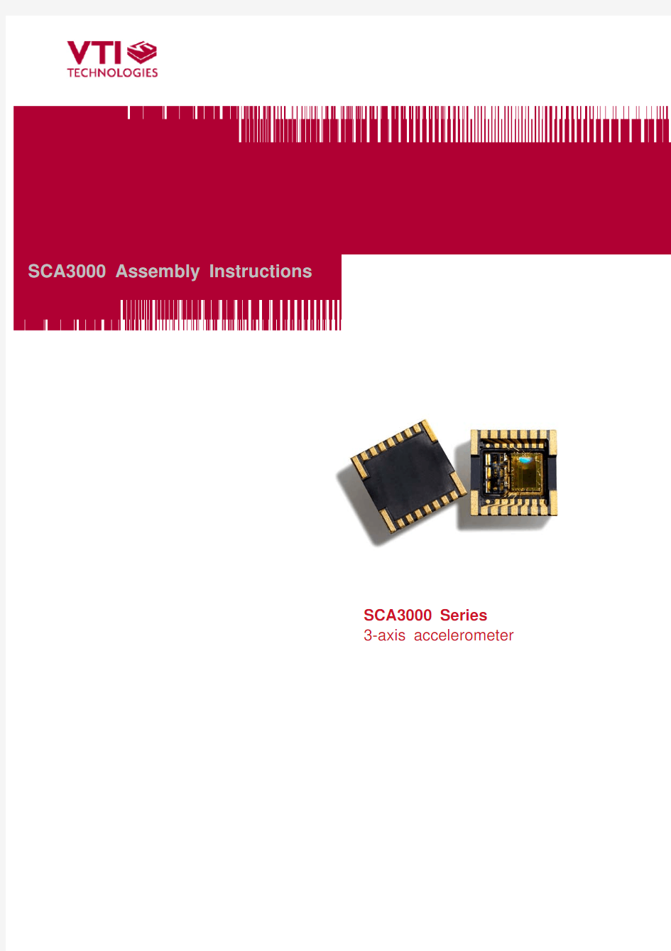
SCA3000 Series
3-axis accelerometer
TABLE OF CONTENTS
1Objective (3)
2VTI's Molded Interconnection Device Package (MID) (3)
3SCA3000 Package Outline and Dimensions (5)
4Tape and reel specifications (6)
5Printed Wiring Board (PWB) Level Guidelines (8)
5.1Land Pad Design (8)
5.2Solder Paste (8)
5.3Stencil (9)
5.4Paste Printing (9)
5.5Component Picking (9)
5.6Component Placement (9)
5.7Reflow Soldering (9)
5.8Moisture sensitivity level (MSL) classification (10)
5.9Inspection (10)
6Rework Guidelines (12)
7Hand Soldering Guidelines (13)
8Environmental Aspects (14)
9References (15)
10Document Revision History (15)
1 Objective
This document describes guidelines for Printed Wiring Board (PWB) design and assembly of the
SCA3000 Component. It aims to help customers achieve the optimum soldering process.
It should be emphasized that this document serves only as a design guideline to help develop the
optimal assembly conditions. It is essential that users also use their own manufacturing practices
and experience to be able to fulfill the needs of varying end-use applications.
2 VTI's Molded Interconnection Device Package (MID)
The housing of the SCA3000 component is relatively new packaging concept, which is called a
molded interconnection device (MID), which is a modified Dual Flat-pack No-lead package (DFN).
The MID housing is leadless component as well as DFN package. The SCA3000 component is a
surface mount plastic package with leads located at the bottom of the package, see picture 1.
Figure 1. 3D pictures of the SCA3000 component. The SCA3000 component leads are located at
the bottom of the package.
MID-technology offers a variety of benefits including reduced lead inductance, a small sized "near
chip scale" footprint, thin profile, and low weight. The MID component is an injection molded plastic
substrate, and the conductive circuit pattern is manufactured on its surface. The SCA3000
component housing is manufactured by the LDS (Laser Direct Structuring) MID-process. The
process flow of LDS - MID package is presented in figure 2.
1. Molding of package
2. Laser structuring of areas to be metallized
3. Cu-plating of lasered areas
4. Final plating over copper
Figure 2.Manufacturing process for the LDS – Molded Interconnect Device.
The solder pads of a MID package are rougher than the pads of traditional lead frame packages. A photo of a MID package solder pad is presented in figure 3. The rougher surface of the solder pad can produce more voids in the solder joints, which is also observed in guidelines of this technical note.
Figure 3. Photo of a MID solder pad. Surface is rougher than with traditional SMD components. Because the MID platform represents the latest in surface mount packaging technology, it is important that the design of the printed wiring board, as well as the assembly process, follows the suggested guidelines outlined in this document.
3 SCA3000 Package Outline and Dimensions
The outline and dimensions for the SCA3000 MID package are presented in figure 4.
0.55 (18x)7.00
0.80
0.80
8 x
= 6.40
0.43 (18x)
2.03 (4x )
1.93 (4x )
0.69 (14x )
0.76 (14x )
5.00
6.24
7.00
6.58
97
°
1.80
0.10
Figure 4. Outline and dimensions of the SCA3000 component.
4 Tape and reel specifications
Packing tape dimensions, unreeling direction and SCA3000 component orientation are presented in figure 5, table 1 and table 2 below (dimensions are in millimeters [mm]).
Table 1. SCA3000 packing tape pocket dimensions [mm].
Direction of unreeling
Pin #1 of SCA3000 component (top view, carrier tape picture not in right scale)
Figure 5. SCA3000 packing tape and component orientation on tape. A0
B0
KO
7.2 ±0.1 7.4 ±0.1
1.9 ±0.1
Table 2. Dimensions for SCA3000 packing tape [mm]. Parameter Min Nominal Max
F 11.40 11.50 11.60 E 1.65 1.75 1.85 W 23.90 24.00 24.30 P2 1.90 2.00 2.10
P0 3.90 4.00 4.10 10P0 39.80 40.00 40.20
D0 1.50 1.50 1.60 D1 1.50 1.50 1.75 T 0.272 0.292 0.312 P 11.90 12.00 12.10
The reel dimensions are presented in figure 6 and table 3 below (dimensions are in millimeters [mm]).
Figure 6. Reel dimensions.
Table 3. SCA3000 Packing reel dimensions [mm].
A N W1 W2max M
330 100 24.4 30.4 ? 13.0
±1 +2.0 -0.2/+0.5
Both tape and reel are ESD materials and they are suitable for baking for 24 hours at +125°C.
5 Printed Wiring Board (PWB) Level Guidelines
5.1 Land Pad Design
Two types of land patterns are used for surface mount packages:
1) Non-Solder Mask Defined Pads (NSMD) 2) Solder Mask Defined Pads (SMD).
NSMD pads have an opening which is larger than the pad itself, and SMD pads have a solder mask opening that is smaller than the metal pad on PWB. NSMD is preferred since the copper etching process has tighter process control compared to the solder mask process. The specific PWB land pattern for the SCA3000 component is presented in figure 7.
Figure 7. Recommended PWB pad layout for SCA3000 component.
VTI's SCA3000 packages can be soldered on commonly used substrates, e.g. FR-4, ceramic etc. The pad metallization should be solder wettable in order to assure good quality solder joints. For fine pitch assembly, the quality of plating is important. Generally used circuit board finishes for fine pitch SMD soldering are NiAu, OSP, Electroless-Ag and Electroless-Sn.
5.2 Solder Paste
The SCA3000 package can be soldered with lead-free SAC (tin-silver-copper) solder. The SAC
solder paste composition should be near eutectic. The melting point of lead-free SAC solder can vary between 217–221oC, depending on the composition of solder alloy. In order to guarantee full RoHS compatibility lead-free solder should be used for the soldering of VTI's SCA3000 component. Also traditional eutectic SnPb solder can be used for soldering the SCA3000 packages if a lead-free process is not required. With the eutectic SnPb solder, the melting point is 183°C.
A no-clean solder paste is recommended, since the SCA3000 package has very small stand off and the effectiveness of cleaning process is therefore low. Ultrasonic agitation wash is not
allowed. The solder paste which is used must be suitable for printing it through the stencil aperture dimensions. Type 3 paste is recommended (grain size 25-45m m).
7.25 mm Pitch 0.976 mm
2.25 mm
0.55 mm
0.25 mm (minimum recommended clearance) Component lead (gray) PWB land (green)
0.10 mm (extension of PWB land towards
center of the package)
0.15 mm (extension of PWB land towards outside of the package)
0,025 mm (extension of
PWB land on both sides)
5.3 Stencil
The solder paste is applied onto the PWB by using stencil printing. The stencil thickness and
aperture determines the precise volume of solder paste deposited onto the land pattern. Stencil
alignment accuracy and consistent solder volume transfer are important parameters for achieving
uniform reflow soldering results. Too much solder paste can cause bridging and too little solder
paste can cause insufficient wetting. Generally the stencil thickness needs to be matched to the
needs of all components on the PWB.
For the SCA3000 MID-package the recommended stencil thickness is 5mils (127μm).
Stencil apertures in general should be 1:1 to PWB pad sizes, or stencil apertures could even be
reduced by 1mil (25.4μm) from all sides in regard to the PWB land pad size. This reduction of
aperture size can reduce bridging between solder joints.
5.4 Paste Printing
The paste printing speed should be adjusted according to the solder paste specifications. It is
recommended that care be taken during paste printing in order to ensure correct paste amount,
shape, position, and other printing characteristics. Neglecting any of these can cause open solder
joints, bridging, solder balling, or other unwanted soldering results.
5.5 Component Picking
The SCA3000 component can be picked from the carrier tape using either vacuum assist or
mechanical type pick heads. Typically a vacuum nozzle is used. Pick up nozzles are available in
various sizes and shapes to suit a variety of different component geometries. It is recommended
that different pick up nozzles are tested to find the best one. The polarity of the part must be
assured in taping process. The polarity of the part on tape is presented in figure 5 on page 4.
5.6 Component Placement
SCA3000 MID packages must be placed onto PWB accurately according to their geometry.
Positioning the packages manually is not recommended. Placement should be done with modern
automatic component pick & place machinery using vision systems.
Recognition of the packages automatically by a vision system enables correct centering of
packages.
5.7 Reflow Soldering
A forced convection reflow oven is recommended to be used for soldering SCA3000 components.
IR-based reflow ovens are not generally suitable for lead-free soldering. Figure 8 presents a
general forced convection reflow solder profile and it also shows the typical phases of a reflow
process.
The reflow profile used for soldering the SCA3000 package should always follow the solder paste
manufacturer's specifications and recommended profile. The typical ramp-up rate is 3°C/second
max. The reflow max. peak temperature (measured from the component body) should not exceed
260°C.The ramp down rate should be 6°C/second max.
Figure 8. Typical convection reflow soldering phases and profile.
The process window for lead-free soldering is narrower than for traditional eutectic SnPb solders.
Thus, caution has to be taken care when adjusting the reflow profiles. The reflow profile should be
measured using a thermo-couple measurement system. It is recommended that at least three
thermo-couples are used, depending on the application. As a general guide, one thermo-couple
should be placed under a component having the largest thermal mass, one next to the smallest
component, one should be in contact with SCA3000 component's solder joint, and others to the
appropriate spots on a circuit board, e.g. corner, center, bottom of the board etc. The reflow profile
should be adjusted according to the measured data so that each solder joint experiences an
optimal reflow profile. The temperature gradient should be as small as possible across the
circuit board and the components. Extreme caution has to be taken if the circuit board
contains components with vastly different thermal masses.
5.8 Moisture sensitivity level (MSL) classification
The Moisture Sensitivity Level of the SCA3000 component is Level 3 according to the IPC/JEDEC
J-STD-020C. The part is delivered in a dry pack. The manufacturing floor time (out of bag) at the
customer’s end is 168 hours. Maximum soldering peak temperature for the SCA3000 is
260°C/40sec, measured from the package body.
5.9 Inspection
Optical and visual inspection of solder joints can be done only partly, since the solder joints are
located underneath the component itself. Therefore inspection of the solder joints with conventional
AOI (automatic optical inspection) system is not recommended. Figure 9 show photos of how the
soldered component on PWB looks from different directions.
Figure 9. Solder pads, component leads and the solder joints are located under the component itself.
X-ray inspection is a recommended inspection method for being able to check the complete solder joint area for solder bridges or short-circuits between solder pads. The X-ray inspection systems vary from manual to fully automated optical inspection systems. X-ray can be used for sample based process control, but it can also be implemented as an automatic in-line control. X-ray inspection can also be used to establish and optimize the component assembly process parameters.
Cross-sectional analysis is also an approved method to inspect how well solder has wetted the
pads of component. Cross-sectional analysis is not used for production inspection, but if required, it can be used to establish and optimize the component assembly process parameters. Cross-sectioning is a destructive inspection method. An example of a SCA3000 solder joint cross-section in presented in figure 10.
Figure 10. Wetting of solder is different on the inner and outer surface of the solder pad.
Outer surface of solder pad
Inner surface of solder pad
6 Rework Guidelines
There are several rework systems on the market. Some will heat solder joints directly from the
sides of component package, while others will direct heat on the top of component. Occasionally,
very rough rework methods are used such as hand placement and heating with a soldering iron.
However, these rough methods are not suitable for VTI's MID components. The heat flow of hot-air
convection should be directed at the edge and under the component body directly to the solder
joints and component pad areas. The package has a limited thermal conductivity and thus, a
horizontal flow method, a conduction method, or a conduction heating from the top of the package
to the solder joints should not be used.
Prior to the rework process, PWBs and components should be free from moisture. If necessary,
baking and drying processes should be performed.
The reflow profile for the component removal should be similar to the initial reflow. A carefully
adjusted reflow profile is essential for the successful rework operation. A proper reflow profile
should be measured with thermo-couples. During the reflow profiling, at least the solder joints, the
top of the component, and the bottom of the PWB should be monitored. If there are other
components near the component to be reworked, the temperatures of those should also be
monitored. The bottom side heating of the PWB is recommended in order to reduce the PWB
warpage during the rework operation.
Once the solder joints have been fully melted, the component can be carefully removed from the
PWB. The common rework methods for the component removal can be used, i.e. a vacuum nozzle
etc. It is absolutely necessary to ensure the complete melting of the solder joints before the
component lifting. If the solder joints are not fully melted before the lifting operation, pad damage
may occur on the PWB and the component.
After the component is removed, the pad areas of the PWB should be cleaned using common
rework methods. These include the applying of a rework flux, an excess solder and flux removal
using a vacuum solder removal tool or a solder wick and a soldering iron with a wide chisel tip, and
the cleaning of solder pads with alcohol and brush. The PWB cleaning process should be
performed gently as too high force or a scrubbing motion can cause pad lifting and trace damage.
If the component reuse is desired, it should be carefully inspected for a potential damage, solder
residues should be removed, and the pads should be cleaned. Prior to the placement of a
replacement component on to the reworked PWB, a solder paste should be applied on the cleaned
PWB pads. Suitable methods for applying the solder paste are the usage of a micro-stencil or the
dispensing of the solder paste. If the micro-stencil is used, it should be cleaned after each paste
application to prevent clogging. For the solder paste and the stencil, the same guidelines as for the
initial reflow process should be used.
The accurate alignment of the component is an important process step thought the surface tension
of the solder during the reflow step will help with the self-alignment. The use of a split-vision
alignment system is recommended to ensure the precise alignment of the component to the PWB.
The "Z" placement force should be carefully controlled in order to prevent the solder bridging.
The same reflow profile, as for the component removal, can be used for the re-attachment of the
replacement component as long as all solder joints will fully melt and properly wet the contact
areas. Otherwise, a new and proper reflow profile must be developed and measured from the
solder joints. The reworked PWBs should be allowed to cool to the room temperature. The PWBs
and the components should be inspected after the rework process for possible defects. The use of
X-ray inspection techniques can be used to verify the success of the rework process.
It should be noted, that the performance and the reliability of the reworked component may have
decreased due to the rework operation.
7 Hand Soldering Guidelines
Hand soldering of the SCA3000 MID package is not recommended. For proto-uses of the SCA3000 component, VTI can provide pre-assembled component on a PWB.
For hand soldering of the SCA3000 component, VTI recommends eutectic tin-lead solder paste due to the lower melting point compared to lead-free solder pastes.
Soldering is possible by applying solder paste onto PWB land pads and then using reflow heating or soldering iron to melt the paste and achieve the soldered joint.
To make the manual hand soldering with soldering iron easier, VTI recommends increasing the PWB land pads length toward the outside of the package by up to 1mm, as shown in Figure 11 below. This extra area is helpful when soldering iron is being used. The hand soldering method is presented in more detail below.
Figure 11. Recommended PWB land pad lengthening for and soldering.
Narrow signal traces to component PWB soldering pads to optimize the conduction of heat to solder paste and component leads. See figure 12 for details.
Figure 12. Narrowed PWB signal traces and use of soldering iron.
1 mm pad extension
Component
lead
PWB soldering Narrow
trace
soldering iron PWB signal trace
1. Apply the solder paste onto the PWB land pads. The paste can be applied by two different
methods.
- Manual solder paste printing through a stencil with normal openings designed for the SCA3000 component.
- Needle dispensing of solder paste manually onto the PWB pads. VTI recommends use of a microscope in manual solder paste dispensing. Dispensing needle tip size can be
0.12"-0.16".
2x amount of solder
paste compared to
smaller PWB
soldering pads
Figure 13: Solder paste (grey) on PWB land pads.
2. Place the component gently on top of the solder paste. To avoid solder bridging, push only very
gently on top of the component.
3. i) Melt the solder paste by putting the part through reflow oven or ii) by using soldering iron.
When using soldering iron, do not touch the package plastic body, soldering iron should touch
only the extension in the PWB's land pad through that the heat should be conducted to melt the
solder paste and then form the solder joint to the component lead. See figure 11 above for
details.
8 Environmental Aspects
VTI Technologies respects environmental values and thus its MID packaged pressure sensors are
lead-free and RoHS compatible. VTI Technologies’ sensors should be soldered with lead-free
solders in order to guarantee full RoHS compatibility.
9 References
JEDEC / Electronic Industries Alliance, Inc. Moisture/ReflowSensitivity Classification for Non-
Hermetic Solid State Surface Mount Devices (J-STD-020C).
10 Document Revision History
Version Date Change Description
Rev. A 30.06.2006 First release
Rev. B 27.09.2006 Rework guidelines added. Corrections to reel dimensions
Rev. C 13.02.2007 Corrections to reflow soldering
VTI Technologies reserves all rights to modify this document without prior notice.