
1
Features
?Dual ADC with 8-bit Resolution
? 1 Gsps Sampling Rate per Channel, 2 Gsps in Interlaced Mode ?Single or 1:2 Demultiplexed Output ?LVDS Output Format (100?)
?500 mVpp Analog Input (Differential Only)?Differential or Single-ended 50? PECL/LVDS Compatible Clock Inputs ?Power Supply: 3.3V (Analog), 3.3V (Digital), 2.25V (Output)?LQFP144 Package ?Temperature Range:
–0°C < TA < 70°C (Commercial Grade)–-40°C < TA < 85°C (Industrial Grade)?3-wire Serial Interface
–16-bit Data, 3-bit Address
–1:2 or 1:1 Output Demultiplexer Ratio Selection –Full or Partial Standby Mode
–Analog Gain (±1.5 dB) Digital Control –Input Clock Selection
–Analog Input Switch Selection –Binary or Gray Logical Outputs –Synchronous Data Ready Reset
–Data Ready Delay Adjustable on Both Channels –Interlacing Functions:
Offset and Gain (Channel to Channel) Calibration
Digital Fine SDA (Fine Sampling Delay Adjust) on One Channel –Internal Static or Dynamic Built-In Test (BIT)
Performance
?Low Power Consumption: 0.7W Per Channel ?Power Consumption in Standby Mode: 120 mW ? 1.5 GHz Full Power Input Bandwidth (-3 dB)
?SNR = 42 dB Typ (6.8 ENOB), THD = -51 dBc, SFDR = -54 dBc at Fs = 1 Gsps Fin = 500 MHz
?2-tone IMD3: -54 dBc (499 MHz, 501 MHz) at 1 Gsps ?DNL = 0.25 LSB, INL = 0.5 LSB
?Channel to Channel Input Offset Error: 0.5 LSB Max (After Calibration) ?Gain Matching (Channel to Channel): 0.5 LSB Max (After Calibration) ?
Low Bit Error Rate (10-13) at 1 Gsps
Application
? Instrumentation ? Satellite Receivers
? Direct RF Down Conversion ?
WLAN
2
AT84AD001B
2153C–BDC–04/04
Description
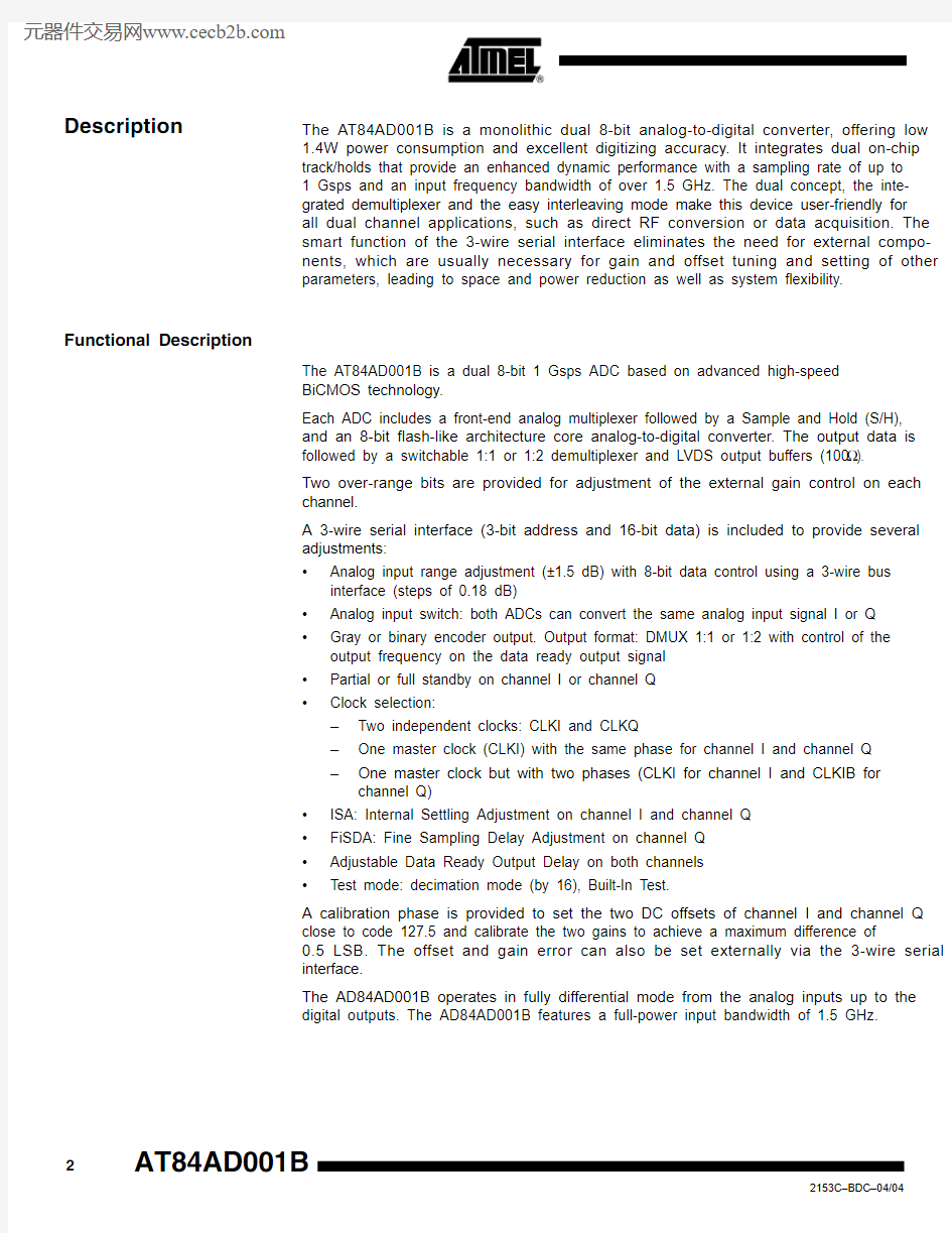
The AT84AD001B is a monolithic dual 8-bit analog-to-digital converter, offering low 1.4W power consumption and excellent digitizing accuracy. It integrates dual on-chip track/holds that provide an enhanced dynamic performance with a sampling rate of up to 1 Gsps and an input frequency bandwidth of over 1.5 GHz. The dual concept, the inte-grated demultiplexer and the easy interleaving mode make this device user-friendly for all dual channel applications, such as direct RF conversion or data acquisition. The smart function of the 3-wire serial interface eliminates the need for external compo-nents, which are usually necessary for gain and offset tuning and setting of other parameters, leading to space and power reduction as well as system flexibility.
Functional Description
The AT84AD001B is a dual 8-bit 1 Gsps ADC based on advanced high-speed BiCMOS technology.
Each ADC includes a front-end analog multiplexer followed by a Sample and Hold (S/H), and an 8-bit flash-like architecture core analog-to-digital converter. The output data is followed by a switchable 1:1 or 1:2 demultiplexer and LVDS output buffers (100?). Two over-range bits are provided for adjustment of the external gain control on each channel.
A 3-wire serial interface (3-bit address and 16-bit data) is included to provide several adjustments: ?Analog input range adjustment (±1.5 dB) with 8-bit data control using a 3-wire bus interface (steps of 0.18 dB)
?Analog input switch: both ADCs can convert the same analog input signal I or Q ?Gray or binary encoder output. Output format: DMUX 1:1 or 1:2 with control of the output frequency on the data ready output signal ?Partial or full standby on channel I or channel Q ?
Clock selection: –Two independent clocks: CLKI and CLKQ
–One master clock (CLKI) with the same phase for channel I and channel Q –One master clock but with two phases (CLKI for channel I and CLKIB for channel Q)
?ISA: Internal Settling Adjustment on channel I and channel Q ?FiSDA: Fine Sampling Delay Adjustment on channel Q ?Adjustable Data Ready Output Delay on both channels ?
Test mode: decimation mode (by 16), Built-In Test.
A calibration phase is provided to set the two DC offsets of channel I and channel Q close to code 127.5 and calibrate the two gains to achieve a maximum difference of 0.5 LSB. The offset and gain error can also be set externally via the 3-wire serial interface.
The AD84AD001B operates in fully differential mode from the analog inputs up to the digital outputs. The AD84AD001B features a full-power input bandwidth of 1.5 GHz.
3
AT84AD001B
2153C–BDC–04/04
Figure 1. Simplified Block Diagram
4
AT84AD001B
2153C–BDC–04/04
Typical Applications
Figure 2. Satellite Receiver Application
5
AT84AD001B
2153C–BDC–04/04
Figure 3. Dual Channel Digital Oscilloscope Application
Note:
Absolute maximum ratings are limiting values (referenced to GND = 0V), to be applied individually, while other parameters are within specified operating conditions. Long exposure to maximum ratings may affect device reliability.
Table 1. Absolute Maximum Ratings
Parameter
Symbol Value Unit Analog positive supply voltage V CCA 3.6V Digital positive supply voltage V CCD 3.6V Output supply voltage
V CCO 3.6V Maximum difference between V CCA and V CCD V CCA to V CCD
± 0.8V Minimum V CCO V CCO 1.6V Analog input voltage V INI or V INIB V INQ or V INQB
1/-1
V Digital input voltage V D
-0.3 to V CCD + 0.3V Clock input voltage
V CLK or VC LKB -0.3 to V CCD + 0.3
V Maximum difference between V CLK and V CLKB V CLK - V CLKB
-2 to 2V Maximum junction temperature T J 125°C Storage temperature
T stg -65 to 150°C Lead temperature (soldering 10s)T leads
300
°C
6
AT84AD001B
2153C–BDC–04/04
Electrical Operating Characteristics
Unless otherwise specified: ?V CCA = 3.3V; V CCD = 3.3V; V CCO = 2.25V
?V INI - V INB or V INQ - V INQB = 500 mVpp full-scale differential input ?LVDS digital outputs (100?)?T A (typical) = 25°C
?
Full temperature range: 0°C < T A < 70°C (commercial grade) or -40°C < T A < 85°C (industrial grade)
Table 2. Recommended Conditions of Use
Parameter
Symbol Comments
Recommended Value
Unit Analog supply voltage V CCA 3.3V Digital supply voltage V CCD 3.3V Output supply voltage
V CCO 2.25V Differential analog input voltage (full-scale)V INi -V IniB or V INQ -V INQB
500mVpp Differential clock input level
Vinclk 600mVpp Internal Settling Adjustment (ISA) with a 3-wire serial interface for channel I and channel Q ISA -50ps Operating temperature range
T Ambient
Commercial grade Industrial grade 0 < T A < 70-40 < T A < 85
°C
Table 3. Electrical Operating Characteristics in Nominal Conditions
Parameter Symbol
Min
Typ Max
Unit Resolution
8
Bits
Power Requirements
Positive supply voltage
- Analog - Digital
Output digital (LVDS) and serial interface V CCA V CCD V CCO 3.153.152.0
3.33.32.25 3.453.452.5V V V
Supply current (typical conditions)
- Analog - Digital - Output I CCA I CCD I CCO
150230100180275120mA mA mA
Supply current (1:2 DMUX mode)
- Analog - Digital - Output
I CCA I CCD I CCO
150260175
180310210
mA mA
7
AT84AD001B
2153C–BDC–04/04
Supply current (2 input clocks, 1:2 DMUX mode)
- Analog - Digital - Output I CCA I CCD I CCO
150290180
180350215
mA
Supply current
(1 channel only, 1:1 DMUX mode)
- Analog - Digital - Output I CCA I CCD I CCO
8016055
9519065
mA mA mA
Supply current
(1 channel only, 1:2 DMUX mode)
- Analog - Digital - Output I CCA I CCD I CCO 801709095205110mA mA mA Supply current (full standby mode)
- Analog - Digital - Output I CCA I CCD I CCO 1224317345mA mA mA Nominal dissipation
(1 clock, 1:1 DMUX mode, 2 channels)P D 1.4 1.7
W Nominal dissipation (full standby mode)stbpd
120
mW
Analog Inputs
Full-scale differential analog input voltage V INi - V IniB
or
V INQ - V INQB
450
500
550
mV
mV
Analog input capacitance I and Q C IN 2
pF Full power input bandwidth (-3 dB)FPBW
1.5GHz Gain flatness (-0.5 dB)500
MHz
Clock Input
Logic compatibility for clock inputs and DDRB Reset (pins 124,125,126,127,128,129)PECL/ECL/LVDS
PECL/LVDS clock inputs voltages (V CLKI/IN or V CLKQ/QN ) Differential logical level V IL - V IH
600mV Clock input power level -9
06
dBm Clock input capacitance 2
pF
Digital Outputs
Logic compatibility for digital outputs (depending on the value of V CCO )LVDS
Differential output voltage swings (assuming V CCO = 2.25V)
V OD
220
270
350
mV
Table 3. Electrical Operating Characteristics in Nominal Conditions (Continued)
Parameter
Symbol Min
Typ Max Unit
8
AT84AD001B
2153C–BDC–04/04
Note:
The gain setting is 0 dB, one clock input, no standby mode [full power mode], 1:1 DMUX, calibration off.
Note:
Gain setting is 0 dB, two clock inputs, no standby mode [full power mode], 1:2 DMUX, calibration on.
Output levels (assuming V CCO = 2.25V) 100? differentially terminated Logic 0 voltage Logic 1 voltage
V OL V OH 1.01.25 1.11.35 1.21.45V V Output offset voltage (assuming V CCO = 2.25V) 100? differentially terminated V OS 1125
12501325
mV Output impedance
R O
50
W
Output current (shorted output)12mA Output current (grounded output)30mA Output level drift with temperature 1.3
mV/°C
Digital Input (Serial Interface)Maximum clock frequency (input clk)Fclk
50MHz Input logical level 0 (clk, mode, data, ldn)-0.400.4V Input logical level 1 (clk, mode, data, ldn)V CCO - 0.4V CCO - 0.4
V CCO + 0.4
V Output logical level 0 (cal)-0.400.4V Output logical level 1 (cal)V CCO - 0.4
V CCO
V CCO + 0.4
V Maximum output load (cal)15
pF
Table 3. Electrical Operating Characteristics in Nominal Conditions (Continued)
Parameter
Symbol
Min
Typ
Max
Unit
Table 4. Electrical Operating Characteristics
Parameter Symbol
Min
Typ
Max
Unit
DC Accuracy No missing code Guaranteed over specified temperature range
Differential non-linearity DNL 0.250.6LSB Integral non-linearity
INL
0.51LSB Gain error (single channel I or Q) with calibration
-0.500.5LSB Input offset matching (single channel I or Q) with calibration -0.5
00.5
LSB Gain error drift against temperature Gain error drift against V CCA
0.0620.064LSB/°C LSB/mV Mean output offset code with calibration 127
127.5
128LSB
Transient Performance Bit Error Rate Fs = 1 Gsps Fin = 250 MHz
BER
10-1310-10
Error/sample
ADC settling time channel I or Q
(between 10% - 90% of output response) V Ini -V iniB = 500 mVpp TS 170ps
9
AT84AD001B
2153C–BDC–04/04
Notes:
1.Differential input [-1 dBFS analog input level], gain setting is 0 dB, two input clock signals, no standby mode,
1:1 DMUX, ISA = -50 ps.
2.Measured on the A T84AD001TD-EB Evaluation Board.
Table 5. AC Performances
Parameter Symbol
Min
Typ
Max
Unit
AC Performance Signal-to-noise Ratio Fs = 1 Gsps Fin = 20 MHz SNR
4244dBc Fs = 1 Gsps Fin = 500 MHz 40
42dBc Fs = 1 Gsps
Fin = 1 GHz
41
dBc
Effective Number of Bits Fs = 1 Gsps Fin = 20 MHz ENOB
77.2Bits Fs = 1 Gsps Fin = 500 MHz 6.5
6.8Bits Fs = 1 Gsps
Fin = 1 GHz
6.2
Bits
Total Harmonic Distortion (First 9 Harmonics)Fs = 1 Gsps Fin = 20 MHz |THD|
4854dBc Fs = 1 Gsps Fin = 500 MHz 45
51dBc Fs = 1 Gsps
Fin = 1 GHz
42
dBc
Spurious Free Dynamic Range Fs = 1 Gsps Fin = 20 MHz |SFDR|
5056dBc Fs = 1 Gsps Fin = 500 MHz 48
54dBc Fs = 1 Gsps
Fin = 1 GHz
43
dBc
Two-tone Inter-modulation Distortion (Single Channel)F IN1 = 499 MHz , F IN2 = 501 MHz at Fs = 1 Gsps IMD
-54dBc Band flatness from DC up to 600 MHz
±0.5
dB
Phase matching using auto-calibration and FiSDA in interlace mode (channel I and Q) Fin = 250 MHz Fs = 1 Gsps
d ?-0.700.7°
Crosstalk channel I versus channel Q Fin = 250 MHz, Fs = 1 Gsps (2)Cr -55dB
10
AT84AD001B
2153C–BDC–04/04
Note:
One analog input on both cores, clock I samples the analog input on the rising and falling edges. The calibration phase is necessary. The gain setting is 0 dB, one input clock I, no standby mode, 1:1 DMUX, FiSDA adjustment.
Table 6. AC Performances in Interlace Mode
Parameter Symbol
Min
Typ
Max
Unit
Interlace Mode
Maximum equivalent clock frequency Fint = 2 x Fs Where Fs = external clock frequency F int 2
Gsps Minimum clock frequency
F int 20Msps Differential non-linearity in interlace mode intDNL 0.25LSB Integral non-linearity in interlace mode intINL
0.5
LSB
Signal-to-noise Ratio in Interlace Mode Fint = 2 Gsps Fin = 20 MHz iSNR
42dBc Fint = 2 Gsps
Fin = 250 MHz
40
dBc
Effective Number of Bits in Interlace Mode Fint = 2 Gsps Fin = 20 MHz iENOB
7.1Bits Fint = 2 Gsps
Fin = 250 MHz
6.8
Bits
Total Harmonic Distortion in Interlace Mode Fint = 2 Gsps Fin = 20 MHz |iTHD|
52dBc Fint = 2 Gsps
Fin = 250 MHz
49
dBc
Spurious Free Dynamic Range in Interlace Mode Fint = 2 Gsps Fin = 20 MHz |iSFDR|
54dBc Fint = 2 Gsps
Fin = 250 MHz
52
dBc
Two-tone Inter-modulation Distortion (Single Channel) in Interlace Mode F IN1 = 249 MHz , F IN2 = 251 MHz at F int = 2 Gsps
iIMD
-54
dBc
11
AT84AD001B
2153C–BDC–04/04
Table 7. Switching Performances
Parameter
Symbol
Min
Typ
Max
Unit
Switching Performance and Characteristics - See “Timing Diagrams” on page 12.Maximum operating clock frequency
F S 1
Gsps Maximum operating clock frequency in BIT and decimation modes
F S (BIT , DEC)
750
Msps Minimum clock frequency (no transparent mode)F S 10Msps Minimum clock frequency (with transparent mode)1Ksps Minimum clock pulse width [high] (No transparent mode)
TC10.40.550ns Minimum clock pulse width [low] (No transparent mode)
TC20.4
0.550
ns Aperture delay: nominal mode with ISA & FiSDA T A 1ns Aperture uncertainty
Jitter 0.4ps (rms)Data output delay between input clock and data TDO 3.8ns Data Ready Output Delay TDR 3ns Data Ready Reset to Data Ready TRDR 2ns Data Output Delay with Data Ready
TD21/2 Fs +Tdrda ps Data Ready (CLKO) Delay Adjust (140 ps steps)Tdrda range
-560 to 420
ps Output skew
50100ps Output rise/fall time for DA T A (20% - 80%)TR/TF 300350500ps Output rise/fall time for DA T A READY (20% - 80%)TR/TF 300
350
500ps
Data pipeline delay (nominal mode)
TPD
3 (port B)
3.5 (port A, 1:1 DMUX mode)4 (port A, 1:2 DMUX mode)Clock cycles
Data pipeline delay (nominal mode) in S/H transparent mode
2.5 (port B)
3 (port A, 1:1 DMUX mode)3.5 (port A, 1:2 DMUX mode)
DDRB recommended pulse width
1
ns
12
AT84AD001B
2153C–BDC–04/04
Timing Diagrams
Figure 4. Timing Diagram, ADC I or ADC Q, 1:2 DMUX Mode, Clock I for ADC I, Clock Q for ADC Q
Figure 5. 1:1 DMUX Mode, Clock I = ADC I, Clock Q = ADC Q
13
AT84AD001B
2153C–BDC–04/04
Figure 6. 1:2 DMUX Mode, Clock I = ADC I, Clock I = ADC Q
14
AT84AD001B
2153C–BDC–04/04
Figure 7. 1:1 DMUX Mode, Clock I = ADC I, Clock I = ADC Q
15
AT84AD001B
2153C–BDC–04/04
Figure 8. 1:2 DMUX Mode, Clock I = ADC I, Clock IN = ADC Q
16
AT84AD001B
2153C–BDC–04/04
Figure 9. 1:1 DMUX Mode, Clock I = ADC I, Clock IN = ADC Q
Figure 10. 1:1 DMUX Mode, Decimation Mode Test (1:16 Factor)
Notes:
1.The maximum clock input frequency in decimation mode is 750 Msps.
2.Frequency(CLKOI) = Frequency(Data) = Frequency(CLKI)/16.
17
AT84AD001B
2153C–BDC–04/04
Figure 11. Data Ready Reset
Figure 12. Data Ready Reset 1:1 DMUX Mode
Note:
The Data Ready Reset is taken into account only 2 ns after it is asserted. The output clock first completes its cycle (if the reset occurs when it is high, it goes low only when its half cycle is complete; if the reset occurs when it is low, it remains low) and then only, remains in reset state (frozen to a low level in 1:1 DMUX mode). The next falling edge of the input clock after reset makes the output clock return to normal mode (after TDR).
FORBIDDEN
FORBIDDEN
18
AT84AD001B
2153C–BDC–04/04
Figure 13. Data Ready Reset 1:2 DMUX Mode
Notes:
1.In 1:2 DMUX, Fs/2 mode:
The Data Ready Reset is taken into account only 2 ns after it is asserted. The output clock first completes its cycle (if the reset occurs when it is low, it goes high only when its half cycle is complete; if the reset occurs when it is high, it remains high) and then only, remains in reset state (frozen to a high level in 1:2 DMUX Fs/2 mode). The next rising edge of the input clock after reset makes the output clock return to normal mode (after TDR).2.In 1:2 DMUX, Fs/4 mode:
The Data Ready Reset is taken into account only 2 ns after it is asserted. The output clock first completes its cycle (if the reset occurs when it is high, it goes low only when its half cycle is complete; if the reset occurs when it is low, it remains low) and then only, remains in reset state (frozen to a low level in 1:2 DMUX Fs/4 mode). The next rising edge of the input clock after reset makes the output clock return to normal mode (after TDR).
19
AT84AD001B
2153C–BDC–04/04
Functions Description
20
AT84AD001B
2153C–BDC–04/04
Digital Output Coding (Nominal Settings)
Pin Description
Table 9. Digital Output Coding (Nominal Setting)
Differential Analog Input Voltage Level
Digital Output I or Q (Binary Coding)
Out-of-range Bit
> 250 mV > Positive full-scale + 1/2 LSB 1 1 1 1 1 1 1 11250 mV 248 mV Positive full-scale + 1/2 LSB Positive full-scale - 1/2 LSB 1 1 1 1 1 1 1 11 1 1 1 1 1 1 0001 mV -1 mV Bipolar zero + 1/2 LSB Bipolar zero - 1/2 LSB 1 0 0 0 0 0 0 00 1 1 1 1 1 1 1 00-248 mV -250 mV Negative full-scale + 1/2 LSB Negative full-scale - 1/2 LSB 0 0 0 0 0 0 0 10 0 0 0 0 0 0 000< -250 mV
< Negative full-scale - 1/2 LSB
0 0 0 0 0 0 0 0
1
Table 10. AT84AD001B LQFP 144 Pin Description
Symbol
Pin number
Function
GNDA, GNDD, GNDO 10, 12, 22, 24, 36, 38, 40, 42, 44, 46, 51, 54, 59, 61, 63, 65, 67, 69, 85, 87, 97, 99, 109, 111, 130, 142, 144Ground pins. T o be connected to external ground plane
V CCA 41, 43, 45, 60, 62, 64
Analog positive supply: 3.3V typical V CCD 9, 21, 37, 39, 66, 68, 88, 100, 112, 123, 141
3.3V digital supply
V CCO 11, 23, 86, 98, 110, 143
2.25V output and 3-wire serial interface supply
V INI 57, 58
In-phase (+) analog input signal of the sample & hold differential preamplifier channel I
V INIB 55, 56
Inverted phase (-) of analog input signal (V INI )
V INQ 47, 48
In-phase (+) analog input signal of the sample & hold differential preamplifier channel Q
V INQB 49, 50Inverted phase (-) of analog input signal (V INQ )
CLKI 124In-phase (+) clock input signal CLKIN 125Inverted phase (-) clock input signal (CLKI)
CLKQ
129
In-phase (+) clock input signal