OCS30
Optical PNPN Switches
GENERAL DESCRIPTION
The OCS30 is an optical switch formed by combining an infrared light emitting diode and a PNPN element (photothyristor) that can withstand high voltages. The device is encased in an 8-pin plastic package. The output PNPN element of the OCS30 forms a bridge configuration,giving the device rectification capabilities.
FEATURES
?Optical switch with photocoupler type 1 ¥ 1 ¥ 2 W (single) bridge ?Available for direct connection to subscriber line
?Total electrical isolation of drive circuit and channel circuit
?Protection function eliminating need for power outage countermeasures ?Simple polarity agreement
?
UL recognized — File number: E86831
APPLICATIONS
?Electronic automatic exchange ?Key telephone system ?Optically coupled circuits
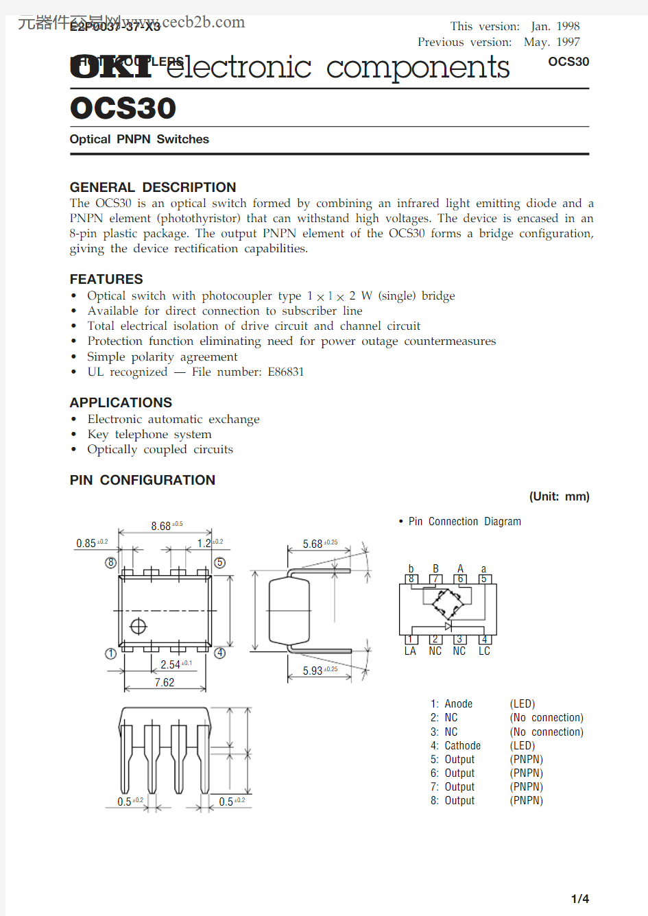
PIN CONFIGURATION
(Unit: mm)
E2P0037-37-X3
1: Anode
2: NC 3: NC
4: Cathode 5: Output 6: Output 7: Output 8: Output (LED)
(No connection)(No connection)(LED)(PNPN)(PNPN)(PNPN)(PNPN)
? Pin Connection Diagram
0°+15–0
0°+15–0
1
8
4
5
8.68±0.5
0.85±0.2
1.2±0.2
5.93±0.25
5.68±0.25
2.54±0.10.5±0.2
0.5±0.27.62
6.4±0.3
7.62±0.15
0.25±0.03
3.65±0.2
4.75m a x .
0.8±0.2
2.8±0.35
This version: Jan. 1998
Previous version: May. 1997
元器件交易网https://www.doczj.com/doc/2612001277.html,
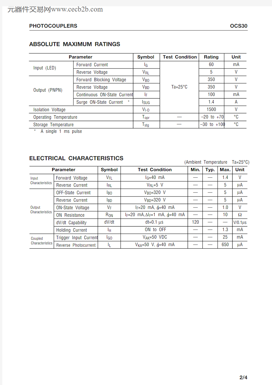
ABSOLUTE MAXIMUM RATINGS
Parameter
Symbol Rating Unit Forward Current Reverse Voltage Forward Blocking Voltage
Reverse Voltage
Continuous ON-State Current I G V RL V BO V BD I F 60mA 5V 350V 350V 100mA * A single 1 ms pulse
Surge ON-State Current *
I SUG 1.4A Isolation Voltage V I-O 1500V Operating Temperature T opr –20 to +70°C Storage Temperature T stg
–30 to +100
°C
Input (LED)
Output (PNPN)
Test Condition
Ta=25°C ——(Ambient Temperature Ta=25°C)
Parameter
Symbol Min.Unit Input
Characteristics
Reverse Current OFF-State Current Reverse Current
ON-State Voltage V FL I RL I BO I BD —V —m A —m A —m A —V Typ.—————Max.1.45551.0Test Condition
I G =40 mA V RL =5 V V BO =320 V V BD =320 V I F =20 mA, I G =40 mA Forward Voltage Output
Characteristics
Coupled
Characteristics
ON Resistance dV/dt Capability Trigger Input Current
Reverse Photocurrent
V F R ON dV/dt I GO I L
I F =20 mA, D I F =1 mA, I G =40 mA
dt=0.1 m s V AK =50 VDC V KA =50 V, I G =40 mA
—W
—10120V/0.1m s
———mA —25—
m A
—
650
Holding Current
I H ON to OFF —mA — 1.3ELECTRICAL CHARACTERISTICS
TYPICAL CHARACTERISTICS
?Continuous ON-State Current vs.
ON-State Voltage (Ta=25°C)?Trigger Input Current vs. Ambient Temperature
Ambient Temperature Ta (°C) T
r
i
g
g
e
r
I
n
p
u
t
C
u
r
r
e
n
t
I
G
O
(
m
A
)
?T rigger Input Current vs. Anode-
Cathode Voltage (Ta=25°C)
?T rigger Input Current vs. Drive Pulse
Width
100
80
60
40
20
20406080100
Anode-Cathode Voltage V AK (V)
T
r
i
g
g
e
r
I
n
p
u
t
C
u
r
r
e
n
t
I
G
O
(
m
A
)
80
60
40
20
Drive Pulse Width tw (m s)
T
r
i
g
g
e
r
I
n
p
u
t
C
u
r
r
e
n
t
I
G
O
(
m
A
)
100
0.1
10
1
0.2
0.5
2
5
20
50
ON-State Voltage V F (V)
C
o
n
t
i
n
u
o
u
s
O
N
-
S
t
a
t
e
C
u
r
r
e
n
t
I
F
(
m
A
)
?Turn On Time vs. LED Forward Current (Ta=25°
C)
40
3020100
102030405060LED Forward Current I G (mA)
T u r n O n T i m e t O N (m s )
?dV/dt Capability vs. Ambient
T
emperature
150
100
50
002040–20
6080
Ambient Temperature Ta (°C)
d V /d t C a p a b i l i t y d V /d t (V /0.1m s )