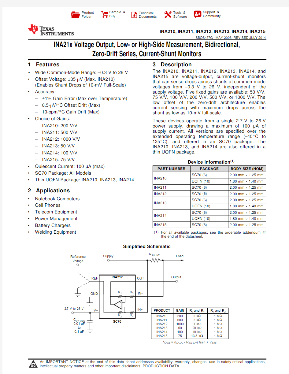

R SHUNT V = (I R ) Gain + V OUT LOAD SHUNT REF
′Product
Folder Sample &Buy Technical
Documents Tools &Software Support &Community
INA210,INA211,INA212,INA213,INA214,INA215
SBOS437G –MAY 2008–REVISED JULY 2014
INA21x Voltage Output,Low-or High-Side Measurement,Bidirectional,
Zero-Drift Series,Current-Shunt Monitors
1Features
3Description The INA210,INA211,INA212,INA213,INA214,and ?
Wide Common-Mode Range:–0.3V to 26V INA215are voltage-output,current-shunt monitors
?Offset Voltage:±35μV (Max,INA210)that can sense drops across shunts at common-mode
(Enables Shunt Drops of 10-mV Full-Scale)voltages from –0.3V to 26V,independent of the
?Accuracy:supply voltage.Five fixed gains are available:50V/V,
75V/V,100V/V,200V/V,500V/V,or 1000V/V.The
–±1%Gain Error (Max over Temperature)low offset of the zero-drift architecture enables
–0.5-μV/°C Offset Drift (Max)current sensing with maximum drops across the
–10-ppm/°C Gain Drift (Max)shunt as low as 10-mV full-scale.
?Choice of Gains:These devices operate from a single 2.7-V to 26-V
–INA210:200V/V power supply,drawing a maximum of 100μA of
supply current.All versions are specified over the
–INA211:500V/V extended operating temperature range (–40°C to
–INA212:1000V/V 125°C),and offered in an SC70package.The
–INA213:50V/V INA210,INA213,and INA214are also offered in a
thin UQFN package.
–INA214:100V/V –INA215:75V/V Device Information (1)
?Quiescent Current:100μA (max)PART NUMBER
PACKAGE BODY SIZE (NOM)?SC70Package:All Models SC70(6) 2.00mm ×1.25mm INA210
?Thin UQFN Package:INA210,INA213,INA214UQFN (10) 1.80mm ×1.40mm INA211
SC70(6) 2.00mm ×1.25mm 2Applications INA212
SC70(6) 2.00mm ×1.25mm ?Notebook Computers SC70(6) 2.00mm ×1.25mm INA213
?Cell Phones UQFN (10) 1.80mm ×1.40mm ?Telecom Equipment SC70(6) 2.00mm ×1.25mm INA214
UQFN (10) 1.80mm ×1.40mm ?Power Management INA215SC70(6) 2.00mm ×1.25mm ?
Battery Chargers (1)For all available packages,see the orderable addendum at
?Welding Equipment the end of the datasheet.
Simplified Schematic
INA210,INA211,INA212,INA213,INA214,INA215
SBOS437G–MAY2008–REVISED https://www.doczj.com/doc/238069198.html,
Table of Contents
8.3Feature Description (13)
1Features (1)
8.4Device Functional Modes (14)
2Applications (1)
9Application and Implementation (20)
3Description (1)
9.1Application Information (20)
4Revision History (2)
9.2Typical Applications (20)
5Device Options (4)
10Power Supply Recommendations (23)
6Pin Configurations and Functions (4)
11Layout (23)
7Specifications (5)
11.1Layout Guidelines (23)
7.1Absolute Maximum Ratings (5)
11.2Layout Example (23)
7.2Handling Ratings (5)
12Device and Documentation Support (24)
7.3Recommended Operating Conditions (6)
12.1Documentation Support (24)
7.4Thermal Information (6)
12.2Related Links (24)
7.5Electrical Characteristics (6)
12.3Trademarks (24)
7.6Typical Characteristics (8)
12.4Electrostatic Discharge Caution (24)
8Detailed Description (12)
12.5Glossary (24)
8.1Overview (12)
13Mechanical,Packaging,and Orderable
8.2Functional Block Diagram (12)
Information (24)
4Revision History
NOTE:Page numbers for previous revisions may differ from page numbers in the current version.
Changes from Revision F(June2014)to Revision G Page ?Changed Simplified Schematic:added equation below gain table (1)
?Changed V(ESD)HBM specifications for version A in Handling Ratings table (5)
Changes from Revision E(June2013)to Revision F Page ?Changed format to meet latest data sheet standards;added Pin Functions,Recommended Operating Conditions, and Thermal Information tables,Overview,Functional Block Diagram,Application Information,Power Supply
Recommendations,and Layout sections,and moved existing sections (1)
?Added INA215to document (1)
?Added INA215sub-bullet to fourth Features bullet (1)
?Added INA215to simplified schematic table (1)
?Changed title of Device Options table (4)
?Added Thermal Information table (5)
?Added INA215to Figure7 (8)
?Added INA215to Figure15 (9)
?Added INA215to Figure25 (16)
Changes from Revision D(November2012)to Revision E Page ?Deleted Package Marking column from Package/Ordering Information table (4)
Changes from Revision C(August2012)to Revision D Page ?Changed Frequency Response,Bandwidth parameter in Electrical Characteristics table (5)
2Submit Documentation Feedback Copyright?2008–2014,Texas Instruments Incorporated
INA210,INA211,INA212,INA213,INA214,INA215 https://www.doczj.com/doc/238069198.html, SBOS437G–MAY2008–REVISED JULY2014
Changes from Revision B(June2009)to Revision C Page
?Changed Package/Ordering table to show both silicon versions A and B (4)
?Added silicon version B ESD ratings to Abs Max table (5)
?Added silicon version B row to Input,Common-Mode Input Range parameter in Electrical Characteristics table (5)
?Corrected typo in Figure9 (8)
?Updated Figure12 (8)
?Changed Input Filtering section (14)
?Added Improving Transient Robustness section (19)
Changes from Revision A(June2008)to Revision B Page
?Added RSW package to device photo (1)
?Added UQFN package to Features list (1)
?Updated front page graphic (1)
?Added RSW ordering information to Package/Ordering Information table (4)
?Added RSW package pin out drawing (4)
?Added footnote3to Electrical Characteristics table (5)
?Added UQFN package information to Temperature Range section of Electrical Characteristics table (5)
?Changed Figure2to reflect operating temperature range (8)
?Changed Figure4to reflect operating temperature range (8)
?Changed Figure6to reflect operating temperature range (8)
?Changed Figure13to reflect operating temperature range (9)
?Changed Figure14to reflect operating temperature range (9)
?Added RSW description to the Basic Connections section (13)
?Changed60μV to100μV in last sentence of the Selecting RS section (13)
Changes from Original(May2008)to Revision A Page
?Changed availability of INA211and INA212to currently available in Package/Ordering Information table (4)
?Deleted first footnote of Electrical Characteristics table (5)
?Changed Figure7 (8)
?Changed Figure15 (9)
Copyright?2008–2014,Texas Instruments Incorporated Submit Documentation Feedback3
NC (1)V+NC (1)IN+
IN+IN -IN -REF 89105431
276GND
OUT 123654OUT IN -IN+
REF
GND V+INA210,INA211,INA212,INA213,INA214,INA215
SBOS437G –MAY 2008–REVISED JULY https://www.doczj.com/doc/238069198.html,
5Device Options
PACKAGE PRODUCT
GAIN (V/V)PACKAGE DESIGNATOR 200SC70-6DCK INA210A
200Thin UQFN-10RSW 200SC70-6DCK INA210B
200Thin UQFN-10RSW INA211A
500SC70-6DCK INA211B
500SC70-6DCK INA212A
1000SC70-6DCK INA212B
1000SC70-6DCK 50SC70-6DCK INA213A
50Thin UQFN-10RSW 50SC70-6DCK INA213B
50Thin UQFN-10RSW 100SC70-6DCK INA214A
100Thin UQFN-10RSW 100SC70-6DCK INA214B
100Thin UQFN-10RSW INA215A 75SC70-6DCK
6Pin Configurations and Functions
DCK Package
RSW Package SC70-6
Thin UQFN-10(Top View)
(Top View)(1)NC denotes no internal connection.These pins can be left floating or connected to any voltage between V–and V+.
4Submit Documentation Feedback Copyright ?2008–2014,Texas Instruments Incorporated
INA210,INA211,INA212,INA213,INA214,INA215 https://www.doczj.com/doc/238069198.html, SBOS437G–MAY2008–REVISED JULY2014
Pin Functions
PIN
NO.I/O DESCRIPTION
NAME
DCK RSW
GND29Analog Ground
Analog
IN–54,5Connect to load side of shunt resistor.
input
Analog
IN+42,3Connect to supply side of shunt resistor
input
NC—1,7—Not internally connected.Leave floating or connect to ground.
Analog
OUT610Output voltage
output
Analog
REF18Reference voltage,0V to V+
input
V+36Analog Power supply,2.7V to26V
7Specifications
7.1Absolute Maximum Ratings(1)
over operating free-air temperature range(unless otherwise noted)
MIN MAX UNIT Supply voltage,V S26V
Differential(V IN+)–(V IN–)–2626V
Analog inputs,V IN+,V IN–(2)
Common-mode(3)GND–0.326V
REF input GND–0.3(V S)+0.3V
Output(3)GND–0.3(V S)+0.3V
Input current into any terminal(3)5mA Operating temperature–55150°C Junction temperature150°C
(1)Stresses beyond those listed under Absolute Maximum Ratings may cause permanent damage to the device.These are stress ratings
only,which do not imply functional operation of the device at these or any other conditions beyond those indicated under Recommended Operating Conditions.Exposure to absolute-maximum-rated conditions for extended periods may affect device reliability.
(2)V IN+and V IN–are the voltages at the IN+and IN–terminals,respectively.
(3)Input voltage at any terminal may exceed the voltage shown if the current at that terminal is limited to5mA.
7.2Handling Ratings
MIN MAX UNIT
T stg Storage temperature range–65150°C
Human body model(HBM)ESD stress voltage(1)–20002000 Electrostatic discharge
V(ESD)Charged-device model(CDM)ESD stress voltage(2)–10001000V (version A)
Machine model(MM)ESD stress voltage–200200
Human body model(HBM)ESD stress voltage(1)–15001500 Electrostatic discharge
V(ESD)Charged-device model(CDM)ESD stress voltage(2)–10001000V (version B)
Machine model(MM)ESD stress voltage–100100
(1)JEDEC document JEP155states that500-V HBM allows safe manufacturing with a standard ESD control process.
(2)JEDEC document JEP157states that250-V CDM allows safe manufacturing with a standard ESD control process.
Copyright?2008–2014,Texas Instruments Incorporated Submit Documentation Feedback5
INA210,INA211,INA212,INA213,INA214,INA215
SBOS437G–MAY2008–REVISED https://www.doczj.com/doc/238069198.html,
7.3Recommended Operating Conditions
over operating free-air temperature range(unless otherwise noted)
MIN NOM MAX UNIT
V CM Common-mode input voltage12V
V S Operating supply voltage5V
T A Operating free-air temperature–40125°C
7.4Thermal Information
INA210-INA215
THERMAL METRIC(1)DCK(SC70)RSW(UQFN)UNIT
6PINS10PINS
RθJA Junction-to-ambient thermal resistance227.3107.3
RθJC(top)Junction-to-case(top)thermal resistance79.556.5
RθJB Junction-to-board thermal resistance72.118.7
°C/W
ψJT Junction-to-top characterization parameter 3.6 1.1
ψJB Junction-to-board characterization parameter70.418.7
RθJC(bot)Junction-to-case(bottom)thermal resistance n/a n/a
(1)For more information about traditional and new thermal metrics,see the IC Package Thermal Metrics application report,SPRA953.
7.5Electrical Characteristics
At T A=25°C,V SENSE=V IN+–V IN–.
INA210,INA213,INA214,and INA215:V S=5V,V IN+=12V,and V REF=V S/2,unless otherwise noted.
INA211and INA212:V S=12V,V IN+=12V,and V REF=V S/2,unless otherwise noted.
PARAMETER CONDITIONS MIN TYP MAX UNIT INPUT
Version A,T A=–40°C to125°C–0.326V
V CM Common-mode input range
Version B,T A=–40°C to125°C–0.126V
INA210,INA211,
V IN+=0V to26V,V SENSE=0mV,
INA212,INA214,105140dB
T A=–40°C to125°C
Common-mode INA215
CMRR
rejection ratio
V IN+=0V to26V,V SENSE=0mV,
INA213100120dB
T A=–40°C to125°C
INA210,INA211,
V SENSE=0mV±0.55±35μV
INA212
V O Offset voltage,RTI(1)
INA213V SENSE=0mV±5±100μV
INA214,INA215V SENSE=0mV±1±60μV
dV OS/dT RTI vs temperature V SENSE=0mV,T A=–40°C to125°C0.10.5μV/°C
V S=2.7V to18V,V IN+=18V,
PSRR RTI vs power supply ratio±0.1±10μV/V
V SENSE=0mV
I IB Input bias current V SENSE=0mV152835μA
I IO Input offset current V SENSE=0mV±0.02μA OUTPUT
INA210200V/V
INA211500V/V
INA2121000V/V
G Gain
INA21350V/V
INA214100V/V
INA21575V/V
V SENSE=–5mV to5mV,
E G Gain error±0.02%±1%
T A=–40°C to125°C
Gain error vs temperature T A=–40°C to125°C310ppm/°C
Nonlinearity error V SENSE=–5mV to5mV±0.01%
Maximum capacitive load No sustained oscillation1nF (1)RTI=referred-to-input.
6Submit Documentation Feedback Copyright?2008–2014,Texas Instruments Incorporated
INA210,INA211,INA212,INA213,INA214,INA215 https://www.doczj.com/doc/238069198.html, SBOS437G–MAY2008–REVISED JULY2014
Electrical Characteristics(continued)
At T A=25°C,V SENSE=V IN+–V IN–.
INA210,INA213,INA214,and INA215:V S=5V,V IN+=12V,and V REF=V S/2,unless otherwise noted.
INA211and INA212:V S=12V,V IN+=12V,and V REF=V S/2,unless otherwise noted.
PARAMETER CONDITIONS MIN TYP MAX UNIT VOLTAGE OUTPUT(2)
R L=10k?to GND,T A=–40°C to
Swing to V+power-supply rail(V+)–0.05(V+)–0.2V
125°C
R L=10k?to GND,T A=–40°C to
Swing to GND(V GND)+0.005(V GND)+0.05V
125°C
FREQUENCY RESPONSE
C LOAD=10pF,INA21014kHz
C LOAD=10pF,INA2117kHz
C LOAD=10pF,INA2124kHz BW Bandwidth
C LOAD=10pF,INA21380kHz
C LOAD=10pF,INA21430kHz
C LOAD=10pF,INA21540kHz
SR Slew rate0.4V/μs NOISE,RTI(1)
Voltage noise density25nV/√Hz POWER SUPPLY
V S Operating voltage range T A=–40°C to125°C 2.726V
I Q Quiescent current V SENSE=0mV65100μA
I Q over temperature T A=–40°C to125°C115μA TEMPERATURE RANGE
Specified range–40125°C
Operating range–55150°C
SC70250°C/W
θJA Thermal resistance
Thin UQFN80°C/W (2)See Typical Characteristic curve,Output Voltage Swing vs Output Current(Figure10).
Copyright?2008–2014,Texas Instruments Incorporated Submit Documentation Feedback7
INA210,INA211,INA212,INA213,INA214,INA215
SBOS437G–MAY2008–REVISED https://www.doczj.com/doc/238069198.html,
7.6Typical Characteristics
The INA210is used for typical characteristics at T A=25°C,V S=5V,V IN+=12V,and V REF=V S/2,unless otherwise noted.
8Submit Documentation Feedback Copyright?2008–2014,Texas Instruments Incorporated
INA210,INA211,INA212,INA213,INA214,INA215 https://www.doczj.com/doc/238069198.html, SBOS437G–MAY2008–REVISED JULY2014
Typical Characteristics(continued)
Copyright?2008–2014,Texas Instruments Incorporated Submit Documentation Feedback9
INA210,INA211,INA212,INA213,INA214,INA215
SBOS437G–MAY2008–REVISED https://www.doczj.com/doc/238069198.html, Typical Characteristics(continued)
10Submit Documentation Feedback Copyright?2008–2014,Texas Instruments Incorporated
INA210,INA211,INA212,INA213,INA214,INA215 https://www.doczj.com/doc/238069198.html, SBOS437G–MAY2008–REVISED JULY2014
Typical Characteristics(continued)
Copyright?2008–2014,Texas Instruments Incorporated Submit Documentation Feedback11
IN-
GND
V+
INA210,INA211,INA212,INA213,INA214,INA215
SBOS437G –MAY 2008–REVISED JULY https://www.doczj.com/doc/238069198.html,
8Detailed Description
8.1Overview
The INA210-INA215are 26-V,common-mode,zero-drift topology,current-sensing amplifiers that can be used in
both low-side and high-side configurations.These specially-designed,current-sensing amplifiers are able to
accurately measure voltages developed across current-sensing resistors on common-mode voltages that far
exceed the supply voltage powering the device.Current can be measured on input voltage rails as high as 26V
while the device can be powered from supply voltages as low as 2.7V.
The zero-drift topology enables high-precision measurements with maximum input offset voltages as low as
35μV with a maximum temperature contribution of 0.5μV/°C over the full temperature range of –40°C to 125°C.
8.2Functional Block Diagram
12Submit Documentation Feedback Copyright ?2008–2014,Texas Instruments Incorporated
Power
Supply INA210,INA211,INA212,INA213,INA214,INA215
https://www.doczj.com/doc/238069198.html, SBOS437G –MAY 2008–REVISED JULY 2014
8.3Feature Description
8.3.1Basic Connections
Figure 23shows the basic connections of the INA210-INA215.The input pins,IN+and IN–,should be connected
as closely as possible to the shunt resistor to minimize any resistance in series with the shunt resistor.
Figure 23.Typical Application
Power-supply bypass capacitors are required for stability.Applications with noisy or high-impedance power
supplies may require additional decoupling capacitors to reject power-supply noise.Connect bypass capacitors
close to the device pins.
On the RSW package options,two pins are provided for each input.These pins should be tied together (that is,
tie IN+to IN+and tie IN–to IN–).
8.3.2Selecting R S
The zero-drift offset performance of the INA210-INA215offers several benefits.Most often,the primary
advantage of the low offset characteristic enables lower full-scale drops across the shunt.For example,non-
zero-drift current shunt monitors typically require a full-scale range of 100mV.
The INA210-INA215series gives equivalent accuracy at a full-scale range on the order of 10mV.This accuracy
reduces shunt dissipation by an order of magnitude with many additional benefits.
Alternatively,there are applications that must measure current over a wide dynamic range that can take
advantage of the low offset on the low end of the measurement.Most often,these applications can use the lower
gains of the INA213,INA214or INA215to accommodate larger shunt drops on the upper end of the scale.For
instance,an INA213operating on a 3.3-V supply could easily handle a full-scale shunt drop of 60mV,with only
100μV of offset.
Copyright ?2008–2014,Texas Instruments Incorporated Submit Documentation Feedback 13
Gain Error Factor =
(1250′
INT
R)
(1250
S
′′′
R) + (1250R) + (R R)
INT S INT
R
V+
INA210,INA211,INA212,INA213,INA214,INA215
SBOS437G–MAY2008–REVISED https://www.doczj.com/doc/238069198.html, 8.4Device Functional Modes
8.4.1Input Filtering
An obvious and straightforward filtering location is at the device output.However,this location negates the advantage of the low output impedance of the internal buffer.The only other filtering option is at the device input pins.This location,though,does require consideration of the±30%tolerance of the internal resistances. Figure24shows a filter placed at the inputs pins.
Figure24.Filter at Input Pins
The addition of external series resistance,however,creates an additional error in the measurement so the value of these series resistors should be kept to10Ωor less if possible to reduce impact to accuracy.The internal bias network shown in Figure24present at the input pins creates a mismatch in input bias currents when a differential voltage is applied between the input pins.If additional external series filter resistors are added to the circuit,the mismatch in bias currents results in a mismatch of voltage drops across the filter resistors.This mismatch creates a differential error voltage that subtracts from the voltage developed at the shunt resistor.This error results in a voltage at the device input pins that is different than the voltage developed across the shunt resistor.Without the additional series resistance,the mismatch in input bias currents has little effect on device operation.The amount of error these external filter resistor add to the measurement can be calculated using Equation2where the gain error factor is calculated using Equation1.
The amount of variance in the differential voltage present at the device input relative to the voltage developed at the shunt resistor is based both on the external series resistance value as well as the internal input resistors,R3 and R4(or R INT as shown in Figure24).The reduction of the shunt voltage reaching the device input pins appears as a gain error when comparing the output voltage relative to the voltage across the shunt resistor.A factor can be calculated to determine the amount of gain error that is introduced by the addition of external series resistance.The equation used to calculate the expected deviation from the shunt voltage to what is seen at the device input pins is given in Equation1:
where:
?R INT is the internal input resistor(R3and R4),and
?R S is the external series resistance.(1) 14Submit Documentation Feedback Copyright?2008–2014,Texas Instruments Incorporated
Gain Error (%) = 100(100Gain Error Factor)-′
INA210,INA211,INA212,INA213,INA214,INA215
https://www.doczj.com/doc/238069198.html, SBOS437G –MAY 2008–REVISED JULY 2014
Device Functional Modes (continued)
With the adjustment factor equation including the device internal input resistance,this factor varies with each
gain version,as shown in Table 1.Each individual device gain error factor is shown in Table 2.
Table 1.Input Resistance
PRODUCT
GAIN R INT (k Ω)INA210
2005INA211
5002INA212
10001INA213
5020INA214
10010INA2157513.3
Table 2.Device Gain Error Factor
The gain error that can be expected from the addition of the external series resistors can then be calculated
based on Equation 2:
(2)
For example,using an INA212and the corresponding gain error equation from Table 2,a series resistance of
10Ωresults in a gain error factor of 0.982.The corresponding gain error is then calculated using Equation 2,
resulting in a gain error of approximately 1.77%solely because of the external 10-Ωseries https://www.doczj.com/doc/238069198.html,ing an
INA213with the same 10-Ωseries resistor results in a gain error factor of 0.991and a gain error of 0.84%again
solely because of these external resistors.
Copyright ?2008–2014,Texas Instruments Incorporated Submit Documentation Feedback 15
Control
INA210,INA211,INA212,INA213,INA214,INA215
SBOS437G –MAY 2008–REVISED JULY https://www.doczj.com/doc/238069198.html,
8.4.2Shutting Down the INA210-INA215Series
While the INA210-INA215series does not have a shutdown pin,its low power consumption allows powering from
the output of a logic gate or transistor switch that can turn on and turn off the INA210-INA215power-supply
quiescent current.
However,in current shunt monitoring applications.there is also a concern for how much current is drained from
the shunt circuit in shutdown conditions.Evaluating this current drain involves considering the simplified
schematic of the INA210-INA215in shutdown mode shown in Figure 25.
NOTE:1-M Ωpaths from shunt inputs to reference and INA21x outputs.
Figure 25.Basic Circuit for Shutting Down the INA210-INA215with a Grounded Reference
Note that there is typically slightly more than 1-M ?impedance (from the combination of 1-M ?feedback and
5-k ?input resistors)from each input of the INA210-INA215to the OUT pin and to the REF pin.The amount of
current flowing through these pins depends on the respective ultimate connection.For example,if the REF pin is
grounded,the calculation of the effect of the 1-M ?impedance from the shunt to ground is straightforward.
However,if the reference or op amp is powered while the INA210-INA215is shut down,the calculation is direct;
instead of assuming 1M ?to ground,however,assume 1M ?to the reference voltage.If the reference or op
amp is also shut down,some knowledge of the reference or op amp output impedance under shutdown
conditions is required.For instance,if the reference source behaves as an open circuit when is not powered,little
or no current flows through the 1-M ?path.
Regarding the 1-M ?path to the output pin,the output stage of a disabled INA210-INA215does constitute a
good path to ground;consequently,this current is directly proportional to a shunt common-mode voltage
impressed across a 1-M ?resistor.
As a final note,when the device is powered up,there is an additional,nearly constant,and well-matched 25μA
that flows in each of the inputs as long as the shunt common-mode voltage is 3V or higher.Below 2-V common-
mode,the only current effects are the result of the 1-M ?resistors.
16Submit Documentation Feedback Copyright ?2008–2014,Texas Instruments Incorporated
INA210,INA211,INA212,INA213,INA214,INA215 https://www.doczj.com/doc/238069198.html, SBOS437G–MAY2008–REVISED JULY2014
8.4.3REF Input Impedance Effects
As with any difference amplifier,the INA210-INA215series common-mode rejection ratio is affected by any impedance present at the REF input.This concern is not a problem when the REF pin is connected directly to most references or power supplies.When using resistive dividers from the power supply or a reference voltage, the REF pin should be buffered by an op amp.
In systems where the INA210-INA215output can be sensed differentially,such as by a differential input analog-to-digital converter(ADC)or by using two separate ADC inputs,the effects of external impedance on the REF input can be cancelled.Figure26depicts a method of taking the output from the INA210-INA215by using the REF pin as a reference.
Figure26.Sensing the INA210-INA215to Cancel the Effects of Impedance on the REF Input
8.4.4Using The INA210-INA215with Common-Mode Transients Above26V
With a small amount of additional circuitry,the INA210-INA215series can be used in circuits subject to transients higher than26V,such as automotive https://www.doczj.com/doc/238069198.html,e only zener diode or zener-type transient absorbers (sometimes referred to as Transzorbs)—any other type of transient absorber has an unacceptable time delay. Start by adding a pair of resistors as a working impedance for the zener;see Figure27.Keeping these resistors as small as possible is preferable,most often around10?.Larger values can be used with an effect on gain that is discussed in the Input Filtering section.Because this circuit is limiting only short-term transients,many applications are satisfied with a10-?resistor along with conventional zener diodes of the lowest power rating that can be found.This combination uses the least amount of board space.These diodes can be found in packages as small as SOT-523or SOD-523.
Copyright?2008–2014,Texas Instruments Incorporated Submit Documentation Feedback17
Shutdown Control R
Shutdown Control R
INA210,INA211,INA212,INA213,INA214,INA215
SBOS437G–MAY2008–REVISED https://www.doczj.com/doc/238069198.html,
Figure27.INA210-INA215Transient Protection using Dual Zener Diodes
In the event that low-power zeners do not have sufficient transient absorption capability and a higher power transzorb must be used,the most package-efficient solution then involves using a single transzorb and back-to-back diodes between the device inputs.The most space-efficient solutions are dual series-connected diodes in a single SOT-523or SOD-523package.This method is shown in Figure28.In either of these examples,the total board area required by the INA210-INA215with all protective components is less than that of an SO-8package, and only slightly greater than that of an MSOP-8package.
Figure28.INA210-INA215Transient Protection using a Single Transzorb and Input Clamps
18Submit Documentation Feedback Copyright?2008–2014,Texas Instruments Incorporated
+2.7V to +26V Reference
Voltage
Shunt Supply Output INA210,INA211,INA212,INA213,INA214,INA215
https://www.doczj.com/doc/238069198.html, SBOS437G –MAY 2008–REVISED JULY 2014
8.4.5Improving Transient Robustness
Applications involving large input transients with excessive dV/dt above 2kV per microsecond present at the
device input pins may cause damage to the internal ESD structures on version A devices.This potential damage
is a result of the internal latching of the ESD structure to ground when this transient occurs at the input.With
significant current available in most current-sensing applications,the large current flowing through the input
transient-triggered,ground-shorted ESD structure quickly results in damage to the silicon.External filtering can
be used to attenuate the transient signal prior to reaching the inputs to avoid the latching condition.Care must be
taken to ensure that external series input resistance does not significantly impact gain error accuracy.For
accuracy purposes,these resistances should be kept under 10Ωif possible.Ferrite beads are recommended for
this filter because of their inherently low dc ohmic value.Ferrite beads with less than 10Ωof resistance at dc
and over 600Ωof resistance at 100MHz to 200MHz are recommended.The recommended capacitor values for
this filter are between 0.01μF and 0.1μF to ensure adequate attenuation in the high-frequency region.This
protection scheme is shown in Figure 29.
Figure 29.Transient Protection
To minimize the cost of adding these external components to protect the device in applications where large
transient signals may be present,version B devices are now available with new ESD structures that are not
susceptible to this latching condition.Version B devices are incapable of sustaining these damage causing
latched conditions so they do not have the same sensitivity to the transients that the version A devices have,
thus making the version B devices a better fit for these applications.Copyright ?2008–2014,Texas Instruments Incorporated Submit Documentation Feedback 19
BYPASS 0.1μF
INA210,INA211,INA212,INA213,INA214,INA215
SBOS437G –MAY 2008–REVISED JULY https://www.doczj.com/doc/238069198.html,
9Application and Implementation
9.1Application Information
The INA210-INA215measure the voltage developed across a current-sensing resistor when current passes
through it.The ability to drive the reference pin to adjust the functionality of the output signal offers multiple
configurations,as discussed throughout this section.
9.2Typical Applications
9.2.1Unidirectional Operation
Figure 30.Unidirectional Application Schematic
9.2.1.1Design Requirements
The device can be configured to monitor current flowing in one direction (unidirectional)or in both directions
(bidirectional)depending on how the REF pin is configured.The most common case is unidirectional where the
output is set to ground when no current is flowing by connecting the REF pin to ground,as shown in Figure 30.
When the input signal increases,the output voltage at the OUT pin increases.
9.2.1.2Detailed Design Procedure
The linear range of the output stage is limited in how close the output voltage can approach ground under zero
input conditions.In unidirectional applications where measuring very low input currents is desirable,bias the REF
pin to a convenient value above 50mV to get the output into the linear range of the device.To limit common-
mode rejection errors,TI recommends buffering the reference voltage connected to the REF pin.
A less frequently-used output biasing method is to connect the REF pin to the supply voltage,V+.This method
results in the output voltage saturating at 200mV below the supply voltage when no differential input signal is
present.This method is similar to the output saturated low condition with no input signal when the REF pin is
connected to ground.The output voltage in this configuration only responds to negative currents that develop
negative differential input voltage relative to the device IN–pin.Under these conditions,when the differential
input signal increases negatively,the output voltage moves downward from the saturated supply voltage.The
voltage applied to the REF pin must not exceed the device supply voltage.
20Submit Documentation Feedback Copyright ?2008–2014,Texas Instruments Incorporated
电流电压功率之间的关 系及公式 LG GROUP system office room 【LGA16H-LGYY-LGUA8Q8-LGA162】
电流、电压、功率的关系及公式 1、电流I,电压V,电阻R,功率W,频率F? W=I2乘以R? V=IR W=V2/R 电流=电压/电阻? 功率=电压*电流*时间 2、电压V(伏特),电阻R(欧姆),电流强度I(安培),功率N (瓦特)之间的关系是: V=IR, N=IV=I*I*R,或也可变形为:I=V/R,I=N/V等等. 但是必须注意,以上均是在直流(更准确的说,是直流稳态)电路情况下推导出来的!其它情况不适用. 如交流电路,那要对其作补充和修正求电压、电阻、电流与功率的换算关系 电流=I,电压=U,电阻=R,功率=P? U=IR,I=U/R,R=U/I,
P=UI,I=P/U,U=P/I? P=U2/R,R=U2/P 还有P=I2RP=IUR=U/I最好用这两个; 3、如电动机电能转化为热能和机械能: 电流符号:I 符号名称:安培(安) 单位:A 公式: 电流=电压/电阻I=U/R 单位换算:1MA(兆安)=1000kA(千安)=1000000A(安) 1A(安)=1000mA(毫安)=1000000μA(微安) 单相电阻类电功率的计算公式=电压U*电流I 单相电机类电功率的计算公式= 电压U*电流I*功率因数COSΦ三相电阻类电功率的计算公式=?*线电压U*线电流I(星形接法) =?3*相电压U*相电I(角形接法)
三相电机类电功率的计算公式=?*线电压U*线电流I*功率因数 COSΦ 星形电流=I,电压=U,电阻=R,功率=P? U=IR,I=U/R,R=U/I, P=UI,I=P/U,U=P/I? P=U2/R,R=U2/P P=I2R? 4、串联电路? P(电功率),U(电压),I(电流),W(电功),R(电阻),T(时间)电流处处相等: I1=I2=I 总电压等于各用电器两端电压之和: U=U1+U2? 总电阻等于各电阻之和: R=R1+R2 U1:U2=R1:R2 总电功等于各电功之和“ W=W1+W2? W1:W2=R1:R2=U1:U2? P1:P2=R1:R2=U1:U2? 总功率等于各功率之和:
LTC2943 - 具温度、电压和电流测量功能的多节电池电量测量芯片 特点 ?可测量累积的电池充电和放电电量 ?至 20V 工作范围可适合多种电池应用 ?14 位 ADC 负责测量电池电压、电流和温度 ?1% 电压、电流和充电准确度 ?±50mV 检测电压范围 ?高压侧检测 ?适合任何电池化学组成和容量的通用测量 ?I2C / SMBus 接口 ?可配置警报输出 / 充电完成输入 ?静态电流小于120μA ?小外形 8 引脚 3mm x 3mm DFN 封装 典型应用 描述 LTC2943可测量便携式产品应用中的电池充电状态、电池电压、电池电流及其自身温度。其具有宽输入电压范围,因而可与高达20V的多节电池配合使用。一个精准的库仑计量器负责对流经位于电池正端子和负载或充电器之间的一个检测电阻器电流进行积分运算。电池电压、电流和温度利用一个内部14位无延迟增量累加(No Latency ΔΣTM) ADC来测量。测量结果被存储于可通过内置I2C / SMBus接口进行存取的内部寄存器中。 LTC2943具有针对所有4种测量物理量的可编程高门限和低门限。如果超过了某个编程门限,则该器件将采用SMBus警报协议或通过在内部状态寄存器中设定一个标记来传送警报信号。LTC2943仅需采用单个低阻值检测电阻器以设定测量电流范围。 应用 ?电动工具 ?电动自行车 ?便携式医疗设备 ?视频摄像机
程序: #include <> #include <> #include "" #include "" #include "" #include "" #include "" #include <> 00; Check I2C Address."; Shared between loop() and restore_alert_settings() .\nPlease ensure I2C lines of Linduino are connected to the LTC device"); } } (ack_error); (F("*************************")); print_prompt(); } } } *\n")); (F("* Set the baud rate to 115200 and select the newline terminator.*\n")); (F("* *\n"));
电流、电压、功率的关系及公式 1、电流I,电压V,电阻R,功率W,频率F W=I2乘以R V=IR W=V2/R 电流=电压/电阻 功率=电压*电流*时间 2、电压V(伏特),电阻R(欧姆),电流强度I(安培),功率N(瓦 特)之间的关系是: V=IR, N=IV=I*I*R,或也可变形为:I=V/R,I=N/V等等. 但是必须注意,以上均是在直流(更准确的说,是直流稳态)电路情况下推导出来的!其它情况不适用. 如交流电路,那要对其作补充和修正求电压、电阻、电流与功率的换算关系 电流=I,电压=U,电阻=R,功率=P U=IR,I=U/R,R=U/I, P=UI,I=P/U,U=P/I P=U2/R,R=U2/P 还有P=I2R P=IU R=U/I 最好用这两个;
3、如电动机电能转化为热能和机械能: 电流符号: I 符号名称: 安培(安) 单位: A 公式: 电流=电压/电阻 I=U/R 单位换算: 1MA(兆安)=1000kA(千安)=1000000A(安)1A(安)=1000mA(毫安)=1000000μA(微安) 单相电阻类电功率的计算公式= 电压U*电流I 单相电机类电功率的计算公式= 电压U*电流I*功率因数COSΦ三相电阻类电功率的计算公式= 1.732*线电压U*线电流I(星形接法) = 3*相电压U*相电I(角形接法)三相电机类电功率的计算公式= 1.732*线电压U*线电流I*功率因数COSΦ 星形电流=I,电压=U,电阻=R,功率=P U=IR,I=U/R,R=U/I, P=UI,I=P/U,U=P/I P=U2/R,R=U2/P P=I2R 4、串联电路 P(电功率),U(电压),I(电流),W(电功),R(电阻),T(时
第一章 电流、电压和功率的测量 1.1 电流的测量 1.1.1 电流表直接测量法 一、直流电流表 1、动圈式磁电系测量机构(“表头”)的工作原理——图1-1-1 “动圈”(即可以转动的线圈)由弹性支承悬挂在永久磁铁产生的磁场中,当 动圈中流过电流i 时,动圈在磁场中受到的电磁力矩为: Ci bNLBi bF M c === 动圈转动时受到弹性支承作用的弹性力矩为: θk M k = 动圈转动时受到与转动角速度成正比的阻尼力矩 dt d D M d θ = c M 驱使动圈转动,而d M 、k M 则阻止线圈转动,因此根据转动定律有: 2 2dt d J M M M d k c θ =-- 将c M 、d M 、k M 代入上式得到动圈式磁电系测量机构的动态方程: Ci k dt d d dt d J =++θθθ22 若信号电流为直流I ,在达到稳定之后,上式左边前两项均为零,于是得到动圈式磁电系测量机构的静态方程: 0CI S I k θ= = 式中S 0=C/k 称为动圈测量机构的静态灵敏度 2、以动圈式磁电系测量机构为“表头”的非电量测量仪表――图0-2(a) 图0-2(a)中传感器的灵敏度(输出电量与输入非电量之比)为S 1,测量电路把 传感器输出的电量转换成直流电流,其灵敏度(输出直流电流与输入电量之比)为S 2,则表头指针偏转角θ与被测非电量x 成线性正比关系。 S x θ=? 式中 012S S S S =为图0-2(a)所示非电量x 的电测仪表的总灵敏度。 2、多量程电流表原理――图1-1—3(b) 单量程交流电流表配接分流电阻即构成多量程交流电流表 若电流表有三挡量程:1I 、2I 、3I ,则量程分流电阻1R 、2R 、3R 满足如下关系式:
毕业设计 微电流检测器设计 指导教师讲师 学院名称工程学院专业名称自动化 论文提交日期2011年5月论文答辩日期2011年5月 答辩委员会主席____________ 评阅人____________ 摘要
近年来,微弱电流信号检测技术在信号处理、电视技术、测量技术、通信技术、信息运算多媒体技术以及一般的电子电路设计等领域得到了非常广泛的应用,并极大地促进了相关技术领域的迅速发展,例如军事侦察、物理学、化学、电化学、生物医学、天文学、地学、磁学等。随着科学技术的发展,对微弱信号进行检测的需要日益迫切,微弱信号检测是发展高新技术、探索及发现新的自然规律的重要手段,对推动相关领域的发展具有重要的意义。 微弱是相对于噪声而言的,所以只靠放大并不能检测出微弱信号,只有在有效地抑制噪声的条件下增大微弱信号的幅度,才能提取出有用信号。因此,必须研究微弱信号检测的理论方法和设备,包括噪声的来源和性质,分析噪声产生的原因和规律以及噪声的传播途径,有针对性地采取有效措施抑制噪声。 本设计制作的微电流检测电路,是以A T89S52芯片为核心实现对微电流信号进行检测并显示,利用两个斩波稳零式高精度运放ICL7650组成的放大模块电路,实现I/V转换,将微电流信号转换成为电压信号,而两个相同高精度运放可以实现对电压信号的一二级放大,经两级放大后的电压通过ADC0809采样、A/D转换后传送给单片机AT89S52,之后单片机经过一些运算编程后控制,将所要测得弱电流信号在LCD1602显示出来。能实现对1uA 到2500uA微电流的实时检测。 关键词:弱电流检测 AT89S52 ICL7650 ADC0809
用多功能电工表检验保护装置能否投入运行 发布时间:2007-1-22 10:50:20 浏览次数:20 古育文广东省梅县供电局(514011) 用负荷电流和工作电压检验是继电保护装置投入运行前的最后一次检查,对于某些保护装置是非常必要的,特别是在带有方向性的继电保护装置中,为了保护其动作正确,在投入运行前必须测量带负荷时的电流与电压的向量图,借此判断电流回路相序、相别及相位是否正确。通过多功能电工表可方便地实现上述功能,替换了以前用相位电压表法和瓦特表法两种繁琐的测量方法。下面结合实际谈谈如何用多功 能电工表来判断方向性的继电保护的接线是否正确。 在2002年10月28日我局所属的一个110kV变电所的电气设备进行电气试验, 经对试验结果进行分析、判断,发现110kV母线的B、C两相电压互感器内部绝 缘介质不良,严重威胁设备的安全运行。为了保证设备的安全运行,对这两相的电压互感器进行了更换。更换后,为了确保继电保护装置的动作正确,我们用多功能电工表(ST9040E型),进行了方向性继电保护装置的电流与电压的相位检查。 1测量方法 在测量前应先找出接入方向性的继电保护装置的电流、电压端子,在电压端子上用相序表检查所接入的电压互感器的二次接线相序应是正序(即是U A-U B-U C)。 然后用多功能电工表的电流测量钳钳住电流端子的A相电流线(假定电流端子接线正确),用多功能电工表的电压测量表笔依次与A、B、C三相的电压端子接触牢靠,将所测得的数据填入表1。用此法依次测量B、C相的电流与电压的相位值,所测得的数据也填入表1。
表1电流、电压和相位值 电压(V) 电流(A) 相位(°) I A=0.9I B=0.91I C=0.9 U A=60197316.873 U B=60.577.8195313.5 U=60 31776.3193 据上表的数据用AUTOCAD2002软件绘出电流向量图,见图1。 图1电流向量图(六角图) 2根据六角图判断接线 六角图作出后,根据测量时的功率的送受情况,判断接线是否正确。这对检验方向 保护,特别是差动保护接线是行之有效的。 功率的送受情况有以下四种: (1)有功与无功功率均从母线送往线路,电流向量应位于第I象限; (2)有功功率从母线送往线路,无功功率由线路送往母线,电流向量应位于第II象
1、欧姆定律: I=U/R U:电压,V; R:电阻,Ω; I:电流,A; 2、全电路欧姆定律: I=E/(R+r) I:电流,A; E:电源电动势,V; r:电源内阻,Ω; R:负载电阻,Ω 3、并联电路,总电流等于各个电阻上电流之和 I=I1+I2+…In 4、串联电路,总电流与各电流相等 I=I1=I2=I3=…=In 5、负载的功率 纯电阻有功功率P=UI → P=I2R(式中2为平方)U:电压,V; I:电流,A; P:有功功率,W; R:电阻 纯电感无功功率 Q=I2*Xl (式中2为平方) Q:无功功率,w; Xl:电感感抗,Ω I:电流,A 纯电容无功功率 Q=I2*Xc (式中2为平方) Q:无功功率,V; Xc:电容容抗,Ω I:电流,A 6、电功(电能) W=UIt W:电功,j; U:电压,V; I:电流,A; t:时间,s 7、交流电路瞬时值与最大 值的关系 I=Imax×sin(ωt+Φ) I:电流,A; Imax:最大电流,A; (ωt+Φ):相位,其中Φ为 初相。 8、交流电路最大值与在效 值的关系 Imax=2的开平方×I I:电流,A; Imax:最大电流,A; 9、发电机绕组三角形联接 I线=3的开平方×I相 I线:线电流,A; I相:相电流,A; 10、发电机绕组的星形联接 I线=I相 I线:线电流,A; I相:相电流,A; 11、交流电的总功率 P=3的开平方×U线×I线 ×cosΦ P:总功率,w; U线:线电压,V; I线:线电流,A; Φ:初相角 12、变压器工作原理 U1/U2=N1/N2=I2/I1 U1、U2:一次、二次电 压,V; N1、N2:一次、二次线圈 圈数; I2、I1:二次、一次电流, A; 13、电阻、电感串联电路 I=U/Z Z=(R2+XL2)和的开平方 (式中2为平方) Z:总阻抗,Ω; I:电流,A; R:电阻,Ω; XL:感抗,Ω 14、电阻、电感、电容串联 电路 I=U/Z Z=[R2+(XL-Xc)2]和的开 平方(式中2为平方) Z:总阻抗,Ω; I:电流,A; R:电阻,Ω; XL:感抗,Ω; Xc:容抗,Ω
课程设计报告题目:电流检测电路设计 课程名称:电子信息工程课程设计 学生姓名:焦道楠 学生学号:1314020114 年级:2013级 专业:电子信息工程 班级:(1)班 指导教师:王留留 电子工程学院制 2016年3月
目录 1 绪论 (1) 2 设计的任务与要求 (1) 2.1 课程设计的任务 (1) 2.2 课程设计的要求 (1) 3 设计方案制定 (1) 3.1 设计的原理 (1) 3.2 设计的技术方案 (2) 4 设计方案实施 (3) 4.1 单片机模块 (3) 4.2 传感器模块 (4) 4.3 A/D转换模块 (5) 4.4 LCD12864点阵液晶显示模块 (6) 5 各模块PCB图 (7) 5.1 单片机模块 (7) 5.2 传感器模块 (7) 6 系统的程序设计 (9) 7 心得体会 (10) 参考文献 (10)
电流检测电路设计 学生:焦道楠 指导教师:王留留 电子工程学院电子信息工程专业 1 绪论 在电学中的测量技术涉及的范围非常广,广泛应用于学校、工业、工厂、科研等各种领域,供实验室和工业现场测量使用。随着电子技术的不断发展,在数字化和智能化不断成为主体的今天,电压、电流测量系统中占有非常重要的位置。我们在分析和总结了单片机技术的发展历史及发展趋势的基础上,以实用、可靠、经济的设计原则为目标,设计出全数字化测量电压电流装置。系统主要以AT89C51单片机为控制核心,整个系统由中央控制模块、A/D转换模块、LED显示模块组成。可实现对待测电压、电流的测量,在数码管上显示。本次课程设计我所做的项目是基于单片机的电流检测系统,主要用到A/D转换和数码管显示。近几年来,单片机已逐步深入应用到工农业生产各部门以及人们生活的各个方面。各种类型的单片机也根据社会的需求而相继开发出来。单片机是一个器件级的计算机系统,实际上它是一个微控制器或微处理器。由于它功能齐全,体积小,成本低,因此它可以应用到所有的电子系统中。AT89C51是一种带4K字节闪存的可编程可插除只读存储器的单片机。单片机的可擦除只读存储器可以反复的擦除多次,该器件采用ATMEL高密度非易失性存储器制造技术制造,与工业标准的MCS-51指令集和输出管脚相兼容。由于将多功能的8位CPU和闪烁存储器组合在单个芯片中,ATMEL的AT89C51是一种高效微控制器。 2设计的任务与要求 2.1 课程设计的任务 利用单片机及其相关知识,设计一个电流检测电路。 2.2 课程设计的要求 (1)画出相应电流检测电路的原理图,并进行检测,生成PCB板; (2)编写程序,实现电流检测功能; (3)情况允许的情况下,做出实物,并估算其成本。 3设计方案制定 3.1 设计的原理
功率电压电流公式功率电压电流公式大全 1、欧姆定律: I=U/R U:电压,V; R:电阻,Ω; I:电流,A; 2、全电路欧姆定律: I=E/(R+r) I:电流,A; E:电源电动势,V; r:电源内阻,Ω; R:负载电阻,Ω 3、并联电路,总电流等于各个电阻上电流之和 I=I1+I2+…In 4、串联电路,总电流与各电流相等 I=I1=I2=I3=…=In 5、负载的功率 纯电阻有功功率P=UI → P=I2R(式中2为平方) U:电压,V; I:电流,A; P:有功功率,W; R:电阻
纯电感无功功率Q=I2*Xl(式中2为平方)Q:无功功率,w; Xl:电感感抗,Ω I:电流,A 纯电容无功功率Q=I2*Xc(式中2为平方)Q:无功功率,V; Xc:电容容抗,Ω I:电流,A 6、电功(电能) W=UIt W:电功,j; U:电压,V; I:电流,A; t:时间,s 7、交流电路瞬时值与最大值的关系 I=Imax×sin(ωt+Φ) I:电流,A; Imax:最大电流,A; (ωt+Φ):相位,其中Φ为初相。 8、交流电路最大值与在效值的关系 Imax=2的开平方×I I:电流,A; Imax:最大电流,A; 9、发电机绕组三角形联接
I线=3的开平方×I相 I线:线电流,A; I相:相电流,A; 10、发电机绕组的星形联接 I线=I相 I线:线电流,A; I相:相电流,A; 11、交流电的总功率 P=3的开平方×U线×I线×cosΦ P:总功率,w; U线:线电压,V; I线:线电流,A; Φ:初相角 12、变压器工作原理 U1/U2=N1/N2=I2/I1 U1、U2:一次、二次电压,V; N1、N2:一次、二次线圈圈数; I2、I1:二次、一次电流,A; 13、电阻、电感串联电路 I=U/Z Z=(R2+XL2)和的开平方(式中2为平方) Z:总阻抗,Ω; I:电流,A; R:电阻,Ω; XL:感抗,Ω 14、电阻、电感、电容串联电路 I=U/Z Z=[R2+(XL-Xc)2]和的开平方(式中2为平方)Z:总阻抗,Ω; I:电流,A; R:电阻,Ω; XL:感抗,Ω; Xc:容抗,Ω
产品特征 显示被测量的变化趋势、读数方便采用夹持式安装方式 技术参数 99T1-A 、V 外型及安装尺寸 96C-A 、V ,96T -A 、V 和96L-Hz 外型及安装尺寸 单位: mm
72L-COS φ外型及安装尺寸 96L-W 、var 外型及安装尺寸 96L-COS φ外型及安装尺寸 72C-A 、V ,72T -A 、V 和72L-Hz 外型及安装尺寸 72L-W 、var 外型及安装尺寸
99T1-A 、V 接线图 接线图 96C-A 、V ,72C-A 、V 接线图
注:带‘*’ 标记的端子为电流进线端96T -A 、V ,72T -A 、V 接线图 96L-Hz ,72L-Hz 接线图 72L-W 、var 接线图
96L-W 、var 接线图 96L-COS Φ接线图 注:带* 标记的端子为电流进线端 注:带*标记的端子为电流进线端
量程参数表(详细信息请参阅固定式直接作用模拟指示电测量仪表附表汇总) 选型指南 备注 1:表内72T -A 和96T -A 交流电流表的所有规格均为2倍电流的过载型 2:交流电流表中,99型的直接接入电流范围为0.5A ~20A ,72型与96型的直接接入电流范围为 1A ~5A 和10A ~100A 3:表中交流电流表0.5A ~20A 用于99T1-A 型, 准确度等级为2.5级,交流电压表99T1-V 型准确 度等级为2.5级 (72型和96型电压表为1.5级)订货示例: 如客户需要99型指针板表,输入方式为交流,类型为电流表,则相对应的订货编码为:99T1A*
功率表如何测功率 F0403014 眭博聪 5040309405 摘要:分析功率表的结构,工作原理及其应用 关键字:功率,功率因素cosφ 前言:在学到三相电路功率测量时,用到了一个新的测量仪表——功率表。但是对于其工作原理,它是怎么可以直接显示功率的大小,为什么要这样接线不甚了解,也为此查阅了些资料。本文介绍了功率表的结构,工作原理等情况。 正文: 功率表是测量直流,交流电路中功率的机械式指示电表。直流电路和交流电路中的功率分别为P=UI。 直流电路和交流电路中的功率分別为P=UI和P=UIcosφ﹐U,I 为负载电压和电流,φ为电流相量与相量间夹角﹐cosφ为功率因数。虽然各系电表的测量机构都有可能构成测量功率的电表﹐但最适于制成功率表的是电动系电表和铁磁电动系电表的测量机构。 功率表的结构: 由于功率表的种类很多,这里只以单相电动系功率表进行分析。 单相电动系功率表的接线原理见图。 这种电表测量机构的转动力矩M与I1I2cosθ有关﹐I1为静圈电流,I2为动圈电流﹐θ为两 电流相量间夹角。使负载电流I通过静圈﹐即I1=I。将负载电压加于动圈及与动圈串联的大电阻R上﹐则动圈中电流I2=U/R。这样θ=φ﹐而转动力矩M=kI1I2cosφ﹐这反映了功率P的大小。 改变与动圈串联的电阻值﹐可改变电压量程﹐将静圈的两线圈由串联改为并联﹐可扩大电流量程。功率表的表盘一般按额定电压与额定电流相乘﹐并使功率因数cosφ=1來标值。如电压量程为300V﹑电流量程为5A的功率表﹐表盘的满刻度值为300×5×1=1500W。也有制成功率因数为 0.1的低功率因数功率表﹐其满刻度值为300×5×0.1=150W。功率表的量程不能简单地只提功率量程﹐而应同時指明电压﹑电流量程及功率因数数值。 功率表的接线: 功率表的正确接法必须遵守“发电机端”的接线规则。 1)功率表标有“*”号的电流端必须接至电源的一端,而另一端则接至负载端。电流线
电流=电压/电阻 功率=电压*电流*时间 电流I,电压V,电阻R,功率W,频率F W=I的平方乘以R V=IR 电流I,电压V,电阻R,功率W,频率F W=I的平方乘以R V=IR W=V的平方除以R 电压V(伏特),电阻R(欧姆),电流强度I(安培),功率N(瓦特)之间的关系是: V=IR,N=IV =I*I*R, 或也可变形为:I=V/R,I=N/V等等.但是必须注意,以上均是在直流(更准确的说,是直流稳态)电路情况下推导出来的!其它情况不适用.如交流电路,那要对其作补充和修正求电压、电阻、电流与功率的换算关系 电流=I,电压=U,电阻=R,功率=P U=IR,I=U/R,R=U/I, P=UI,I=P/U,U=P/I P=U2/R,R=U2/P 就记得这一些了,不知还有没有 还有P=I2R P=IU R=U/I 最好用这两个;如电动机电能转化为热能和机械能。电流 符号: I 符号名称: 安培(安) 单位: A 公式: 电流=电压/电阻 I=U/R 单位换算: 1MA(兆安)=1000kA(千安)=1000000A(安) 1A(安)=1000mA(毫安)=1000000μA(微安)单相电阻类电功率的计算公式= 电压U*电流I
单相电机类电功率的计算公式= 电压U*电流I*功率因数COSΦ 三相电阻类电功率的计算公式= *线电压U*线电流I (星形接法) = 3*相电压U*相电流I(角形接法) 三相电机类电功率的计算公式= *线电压U*线电流I*功率因数COSΦ(星形电流=I,电压=U,电阻=R,功率=P U=IR,I=U/R,R=U/I, P=UI,I=P/U,U=P/I P=U2/R,R=U2/P 就记得这一些了,不知还有没有 还有P=I2R ⑴串联电路 P(电功率)U(电压)I(电流)W(电功)R(电阻)T(时间) 电流处处相等 I1=I2=I 总电压等于各用电器两端电压之和 U=U1+U2 总电阻等于各电阻之和 R=R1+R2 U1:U2=R1:R2 总电功等于各电功之和 W=W1+W2 W1:W2=R1:R2=U1:U2 P1:P2=R1:R2=U1:U2 总功率等于各功率之和 P=P1+P2 ⑵并联电路 总电流等于各处电流之和 I=I1+I2 各处电压相等 U1=U1=U 总电阻等于各电阻之积除以各电阻之和R=R1R2÷(R1+R2) 总电功等于各电功之和 W=W1+W2 I1:I2=R2:R1 W1:W2=I1:I2=R2:R1 P1:P2=R2:R1=I1:I2 总功率等于各功率之和 P=P1+P2
Application Circuit STMC109 SOT23 109 DC Motor Control Programmable Current Source Level Translating Over Current Monitor SOT23 Package SOT23 packages. The STMC109is a high side current sense monitor.STMC109 1 DESCRIPTION Using this device eliminates the need to disrupt the ground plane when sensing a load current. It takes a high side voltage developed across a current shunt resistor and translates it into a proportional output current. A user defined output resistor scales the output current into a ground-referenced voltage. The wide input voltage range of 20V down to as low as 2.5V make it suitable for a range of applications.A minimum operating current of just 4μA,combined with its SOT23package make it a unique solution,suitable for portable battery equipment.FEATURES ?Low cost, accurate high-side current sensing.?Output voltage scaling.?Up to 2.5V sense voltage.? 2.5V – 20V supply range.?4μA quiescent current.?1% typical accuracy.? APPLICATIONS ?Battery Chargers ?Smart Battery Packs ???Power Management ?? HIGH-SIDE CURRENT MONITOR V To Load R ORDERING INFORMATION PART NUMBER PACKAGE PARTMARKING Top View I out Load V in 3 2 1 CONNECTION DIAGRAMS ABSOLUTE MAXIMUM RATINGS Voltage on any pin -0.6V to 20V (relative to I out )Continuous output current 25mA Continuous sense voltage V in + 0.5V > V sense ?> V in – 5V Operating Temperature -40 to 85°C Storage Temperature -55 to 125°C Package Power Dissipation (T A = 25°C)SOT23 450mW
电机转矩功率转速电压电流之间的关系及计算 公式 Document serial number【NL89WT-NY98YT-NC8CB-NNUUT-NUT108】
电机转矩、功率、转速之间的关系及计算公式 电动机输出转矩: 使机械元件转动的力矩称为转动力矩,简称转矩。机械元件在转矩作用下都会产生一定程度的扭转变形,故转矩有时又称为扭矩。 转矩与功率及转速的关系:转矩(T)=9550*功率(P)/转速(n) 即:T=9550P/n—公式【1】 由此可推导出: 转矩=9550*功率/转速《===》功率=转速*转矩/9550,即P=Tn/9550——公式 【2】 方程式中: P—功率的单位(kW); n—转速的单位(r/min); T—转矩的单位(N.m); 9550是计算系数。 电机扭矩计算公式 T=9550P/n 是如何计算的呢? 分析: 功率=力*速度即 P=F*V---————公式【3】 转矩(T)=扭力(F)*作用半径(R) 推出F=T/R---——公式【4】 线速度(V)=2πR*每秒转速(n秒)=2πR*每分转速(n分)/60=πR*n分/30---——公式【5】 将公式【4】、【5】代入公式【3】得: P=F*V=T/R*πR*n分/30 =π/30*T*n分 -----P=功率单位W, T=转矩单位N.m, n分=单位转/分钟 如果将P的单位换成KW,那么就是如下公式: P*1000=π/30*T*n 30000/π*P=T*n30000/3.1415926*P=T*n9549.297*P=T*n 这就是为什么会有功率和转矩*转速之间有个9550的系数关系。。。 电动机转矩、转速、电压、电流之间的关系 由于电功率P=电压U*电流I,即 P=UI————公式【6】 由于公式【2】中的功率P的单位为kw,而电压U的单位是V,电流I的单位是A,而UI 乘积的单位是V.A,即w,所以将公式【6】代入到公式【2】中时,UI需要除以1000以统一单位。 则: P=Tn/9550=UI/1000————公式【7】 ==》Tn/9.55=UI————公式【8】 ==》T=9.55UI/n————公式【9】 ==》U=Tn/9.55I————公式【10】 ==》I=9.55U/Tn————公式【11】 方程式【7】、【8】、【9】、【10】、【11】中: P—功率的单位(kW);
变频器中的频率、电压、转速、电流、功率,转矩的关系 异步电动机的转矩是电机的磁通与转子内流过电流之间相互作用而产生的,在额定频率下,如果电压一定而只降低频率,那么磁通就过大,磁回路饱和,严重时将烧毁电机。因此,频率与电压要成比例地改变,即改变频率的同时控制变频器输出电压,使电动机的磁通保持一定,避免弱磁和磁饱和现象的产生。这种控制方式多用于风机、泵类节能型变频器。 频率下降时电压V也成比例下降,这个问题已在回答4说明。V与f的比例关系是考虑了电机特性而预先决定的,通常在控制器的存储装置(ROM)中存有几种特性,可以用开关或标度盘进行选择。 频率下降时完全成比例地降低电压,那么由于交流阻抗变小而直流电阻不变,将造成在低速下产生地转矩有减小的倾向。因此,在低频时给定V/f,要使输出电压提高一些,以便获得一定地起动转矩,这种补偿称增强起动。可以采用各种方法实现,有自动进行的方法、选择V/f模式或调整电位器等方法。 一、引言 随着变频调速技术的发展,变频器调速已成为交流调速的主流,在化纤、纺织、钢铁、机械、造纸等行业得到广泛的应用。由于通用变频器一般采用V/f控制,即变压变频(VVVF)方式调速,因此,变频器在使用前正确地设定其压频比,对保证变频器的正常工作至关重要。变频器的压频比由变频器的基准电压与基准频率两项功能参数的比值决定,即基准电压/基准频率=压频比。 基准电压与基准频率参数的设定,不仅与电动机的额定电压与额定频率有关(电机的压频比为电机的额定电压与额定频率之比),而且还必须考虑负载的机械特性。对于普通异步电机在一般调速应用时,其基准电压与基准频率按出厂值设定(基准电压380V,基准频率50Hz),即满足使用要求。但对于某些行业使用的较特殊的电机,就必须根据实际情况重新设定基准电压与基准频率的参数。由于变频器使用说明书以及有关书籍中没有对这两个参数作详细介绍,因此正确的设定该参数对于不少使用者来说,并非很容易的事。为此,本文结合变频调速的基本控制方式及负载的机械特性与基准电压、基准频率参数的关系,列举实例,详细说明基准电压与基准频率参数的设定方法。 二、变频调速的基本控制方式与基准电压、基准频率的关系 电机用变频器调速时有两种情况‐‐基频(基准频率)以下调速和基频以上调速(见图1)。必须考虑的重要因素是:尽量保持电机主磁通为额定值不变。如果磁通过弱(电压过低),电机铁心不能得到充分利用,电磁转矩变小,负载能力下降。如果磁通过强(电压过高),电机处于过励磁状态,电机因励磁电流过大而严重发热。根据电机原理可知,三相异步电机定子每相电动势的有效值 : E1=4.44f1N1Φm 式中 :E1‐‐定子每相由气隙磁通感应的电动势的有效值,V ;f1‐‐定子频率,Hz;N1——定子每相绕组有效匝数 ;Φm‐每极磁通量 由式中可以看出,Φm的值由E1/f1决定,但由于E1难以直接控制,所以在电动势较高时,可忽略定子漏阻抗压降,而用定子相电压U1代替。那么要保证Φm不变,只要U1/f1始终为一定值即可。这是基频以下调时速的基本情况,为恒压频比(恒磁通)控制方式,属于恒转 矩调速。从图1可以看出,基准频率为恒转矩调速区的最高频率,基准频率所对应的电压为即为基准电压,是恒转矩调速区的最高电压,在基频以下调速时,电压会随频率而变化,但两 者的比值不变。 在基频以上调速时,频率从基频向上可以调至上限频率值,但是由于电机定子不能超过 电机额定电压,因此电压不再随频率变化,而保持基准电压值不变,这时电机主磁通必须随频率升高而减弱,转矩相应减小,功率基本保持不变,属于恒 功率调速区。由图1可见,基准频率为恒功率调速区的最低频率,是恒转矩调速区与恒功率调速区的转折
单相电路参数测量及功率因数的提高 一实验目的 1.掌握单相功率表的使用。 2.了解日光灯电路的组成、工作原理和线路的连接。 3.研究日光灯电路中电压、电流相量之间的关系。 4.理解改善电路功率因数的意义并掌握其应用方法。 二实验原理 1.日光灯电路的组成 日光灯电路是一个RL串联电路,由灯管、镇流器、起辉器组成,如图3-1所示。由于有感抗元件,功率因数较低,提高电路功率因数实验可以用日光灯电路来验证。 I 图3-1日光灯的组成电路 灯管:内壁涂上一层荧光粉,灯管两端各有一个灯丝(由钨丝组成),用以发射电子,管内抽真空后充有一定的氩气与少量水银,当管内产生辉光放电时,发出可见光。 镇流器:是绕在硅钢片铁心上的电感线圈。它有两个作用,一是在起动过程中,起辉器突然断开时,其两端感应出一个足以击穿管中气体的高电压,使灯管中气体电离而放电。二是正常工作时,它相当于电感器,与日光灯管相串联产生一定的电压降,用以限制、稳定灯管的电流,故称为镇流器。实验时,可以认为镇流器是由一个等效电阻R L和一个电感L串联组成。 起辉器:是一个充有氖气的玻璃泡,内有一对触片,一个是固定的静触片,一个是用双金属片制成的U形动触片。动触片由两种热膨胀系数不同的金属制成,受热后,双金属片伸张与静触片接触,冷却时又分开。所以起辉器的作用是使电路接通和自动断开,起一个自动开关作用。 2.日光灯点亮过程 电源刚接通时,灯管内尚未产生辉光放电,起辉器的触片处在断开位置,此
时电源电压通过镇流器和灯管两端的灯丝全部加在起辉器的二个触片上,起辉器的两触片之间的气隙被击穿,发生辉光放电,使动触片受热伸张而与静触片构成通路,于是电流流过镇流器和灯管两端的灯丝,使灯丝通电预热而发射热电子。与此同时,由于起辉器中动、静触片接触后放电熄灭,双金属片因冷却复原而与静触片分离。在断开瞬间镇流器感应出很高的自感电动势,它和电源电压串联加到灯管的两端,使灯管内水银蒸气电离产生弧光放电,并发射紫外线到灯管内壁,激发荧光粉发光,日光灯就点亮了。 灯管点亮后,电路中的电流在镇流器上产生较大的电压降(有一半以上电压),灯管两端(也就是起辉器两端)的电压锐减,这个电压不足以引起起辉器氖管的辉光放电,因此它的两个触片保持断开状态。即日光灯点亮正常工作后,起辉器不起作用。 3.日光灯的功率因数 日光灯点亮后的等效电路如图2 所示。灯管相当于电阻负载R A ,镇流器用内阻R L 和电感L 等效代之。由于镇流器本身电感较大,故整个电路功率因数很低,整个电路所消耗的功率P 包括日光灯管消耗功率P A 和镇流器消耗的功率P L 。只要测出电路的功率P 、电流I 、总电压U 以及灯管电压U R ,就能算出灯管消耗的功率P A =I ×U R , 镇流器消耗的功率P L =P ?P A ,UI P =?cos R A 图3-2日光灯工作时的等效电路 2.功率因数的提高 日光灯电路的功率因数较低,一般在0.5 以下,为了提高电路的功率因数,可以采用与电感性负载并联电容器的方法。此时总电流I 是日光灯电流 I L 和电容器电流 I C 的相量和:? ? ? +=C L I I I ,日光灯电路并联电容器后的相量图如图3 所示。由于电容支路的电流I C 超前于电压U 90°角。抵消了一部分日光灯支路电流中的无功分量,使电路的总电流I 减小,从而提高了电路的功率因数。电压与电流的相位差角由原来的 1?减小为?,故cos ?>cos 1?。 当电容量增加到一定值时,电容电流C I 等于日光灯电流中的无功分量,?= 0。cos ?=1,此时总电流下降到最小值,整个电路呈电阻性。若继续增加电容量,
---------------------------------------------------------------最新资料推荐------------------------------------------------------ 电流检测器件分析 电流检测器件分析一、检测电阻+运放优势: 成本低、精度较高、体积小劣势: 温漂较大,精密电阻的选择较难,无隔离效果。 分析: 这两种拓扑结构,都存在一定的风险性,低端检测电路易对地线造成干扰;高端检测,电阻与运放的选择要求高。 检测电阻,成本低廉的一般精度较低,温漂大,而如果要选用精度高的,温漂小的,则需要用到合金电阻,成本将大大提高。 运放成本低的,钳位电压低,而特殊工艺的,则成本上升很多。 二、电流互感器 CT/电压互感器 PT 在变压器理论中,一、二次电压比等于匝数比,电流比为匝数比的倒数。 而 CT 和 PT就是特殊的变压器。 基本构造上, CT 的一次侧匝数少,二次侧匝数多,如果二次开路,则二次侧电压很高,会击穿绕阻和回路的绝缘,伤及设备和人身。 PT 相反,一次侧匝数多,二次侧匝数少,如果二次短路,则二次侧电流很大,使回路发热,烧毁绕阻及负载回路电气。 CT,电流互感器,英文拼写 Current Transformer,是将 1 / 10
一次侧的大电流,按比例变为适合通过仪表或继电器使用的,额定电流为 5A 或 1A 的变换设备。 它的工作原理和变压器相似。 也称作 TA 或 LH(旧符号)工作特点和要求: 1、一次绕组与高压回路串联,只取决于所在高压回路电流,而与二次负荷大小无关。 2、二次回路不允许开路,否则会产生危险的高电压,危及人身及设备安全。 3、 CT 二次回路必须有一点直接接地,防止一、二次绕组绝缘击穿后产生对地高电压,但仅一点接地。 4、变换的准确性。 PT,电压互感器,英文拼写 Phase voltage Transformers,是将一次侧的高电压按比例变为适合仪表或继电器使用的额定电压为 100V 的变换设备。 电磁式电压互感器的工作原理和变压器相同。 也称作 TV 或 YH(旧符号)。 工作特点和要求: 1、一次绕组与高压电路并联。 2、二次绕组不允许短路(短路电流烧毁 PT) ,装有熔断器。 3、二次绕组有一点直接接地。 4、变换的准确性三、模块型霍尔电流传感器模块型
电流I,电压V,电阻R,功率W,频率F W=I的平方乘以R V=IR W=V的平方除以R 电流=电压/电阻 功率=电压*电流*时间 电流I,电压V,电阻R,功率W,频率F W=I的平方乘以R V=IR 电流I,电压V,电阻R,功率W,频率F W=I的平方乘以R V=IR W=V的平方除以R 电压V(伏特),电阻R(欧姆),电流强度I(安培),功率N(瓦特)之间的关系是:V=IR,N=IV =I*I*R, 或也可变形为:I=V/R,I=N/V等等.但是必须注意,以上均是在直流(更准确的说,是直流稳态)电路情况下推导出来的!其它情况不适用.如交流电路,那要对其作补充和修正求电压、电阻、电流与功率的换算关系 电流=I,电压=U,电阻=R,功率=P U=IR,I=U/R,R=U/I, P=UI,I=P/U,U=P/I P=U2/R,R=U2/P
就记得这一些了,不知还有没有 还有P=I2R P=IU R=U/I 最好用这两个;如电动机电能转化为热能和机械能。电流 符号: I 符号名称: 安培(安) 单位: A 公式: 电流=电压/电阻I=U/R 单位换算: 1MA(兆安)=1000kA(千安)=1000000A(安) 1A(安)=1000mA(毫安)=1000000μA(微安)单相电阻类电功率的计算公式= 电压U*电流I 单相电机类电功率的计算公式= 电压U*电流I*功率因数COSΦ 三相电阻类电功率的计算公式= 1.732*线电压U*线电流I (星形接法) = 3*相电压U*相电流I(角形接法) 三相电机类电功率的计算公式= 1.732*线电压U*线电流I*功率因数COSΦ(星形电流= I,电压=U,电阻=R,功率=P U=IR,I=U/R,R=U/I, P=UI,I=P/U,U=P/I P=U2/R,R=U2/P 就记得这一些了,不知还有没有 还有P=I2R ⑴串联电路P(电功率)U(电压)I(电流)W(电功)R(电阻)T(时间)电流处处相等I1=I2=I 总电压等于各用电器两端电压之和U=U1+U2 总电阻等于各电阻之和R=R1+R2