
Specifications Subject to Change Without Notice.
1400 - 2000 MHz
Features
? Low Noise Figure:
1.6dB
? High Input IP3:-6dBm at 3V,6.5mA bias ? High Gain:18dB
? Single Supply:+3to +8VDC
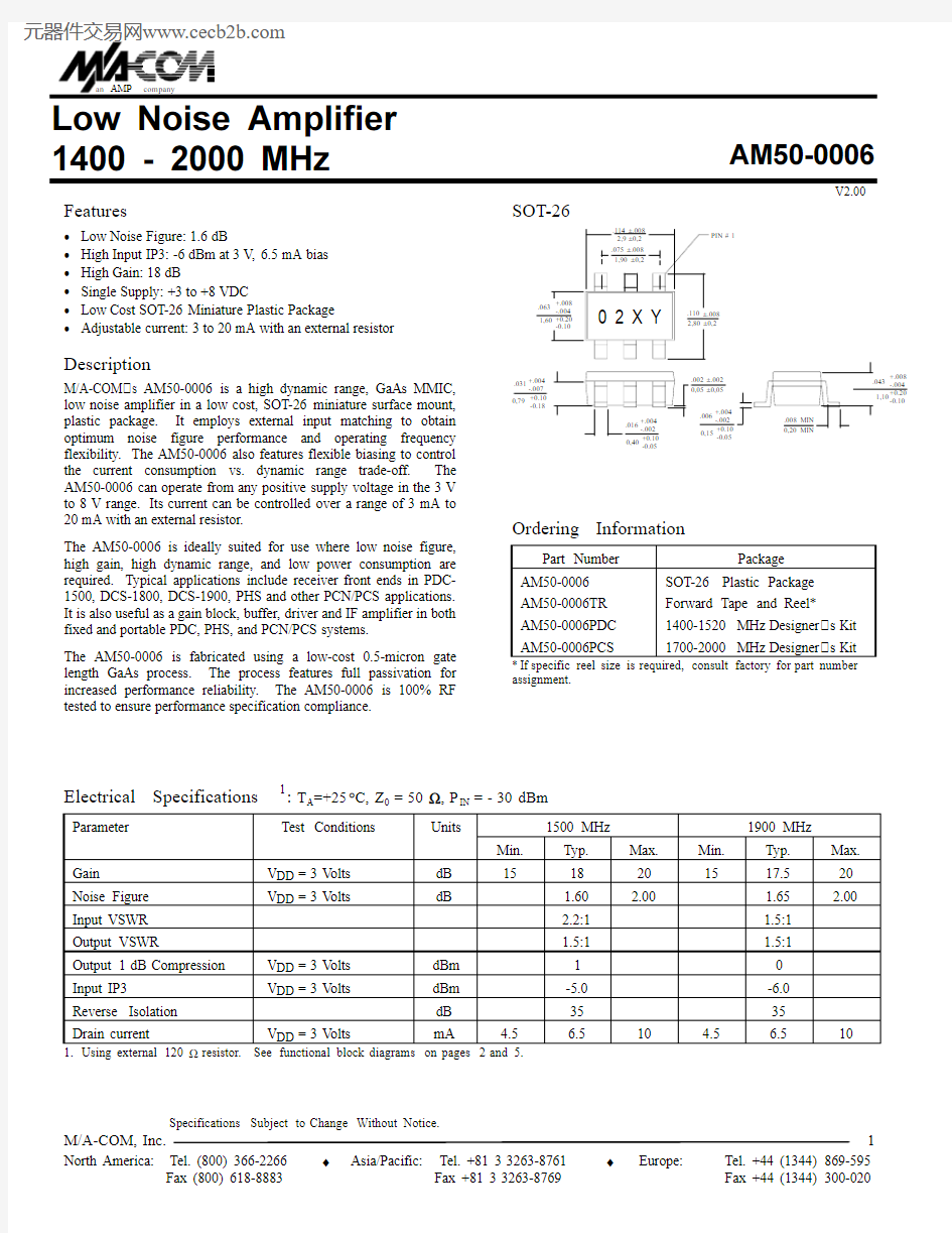
? Low Cost SOT-26Miniature Plastic Package
?
Adjustable current:3to 20mA with an external resistor
Description
M/A-COM s AM50-0006is a high dynamic range,GaAs MMIC,low noise amplifier in a low cost,SOT-26miniature surface mount,plastic package.It employs external input matching to obtain optimum noise figure performance and operating frequency flexibility.The AM50-0006also features flexible biasing to control the current consumption vs.dynamic range trade-off.The AM50-0006can operate from any positive supply voltage in the 3V to 8V range.Its current can be controlled over a range of 3mA to 20mA with an external resistor.
The AM50-0006is ideally suited for use where low noise figure,high gain,high dynamic range,and low power consumption are required.Typical applications include receiver front ends in PDC-1500,DCS-1800,DCS-1900,PHS and other PCN/PCS applications.It is also useful as a gain block,buffer,driver and IF amplifier in both fixed and portable PDC,PHS,and PCN/PCS systems.
The AM50-0006is fabricated using a low-cost 0.5-micron gate length GaAs process.The process features full passivation for increased performance reliability.The AM50-0006is 100%RF tested to ensure performance specification compliance.
SOT-26
-0.05
assignment.
Electrical Specifications 1
:T A =+25°C,Z 0=50?,P IN =-30
dBm
Specifications Subject to Change Without Notice.
1
cause permanent damage.
2.When pin #2is used to increase current.(See note 5.)
3.Thermal resistance (θjc)=+150°C/W.
Functional Block Diagram For 1700-2000MHz Operation
Recommended PCB Configuration For 1700-2000MHz Operation
Layout View
Input Reflection Coefficient 1700-2000MHz Operation
External Circuitry Parts List For
4
4.All external circuitry parts are readily available,low cost surface mount components (.060in.x .030in.or .080in.x .050in.).
5.Pin 2allows use of an external resistor to ground for optional,higher current.
For I ,,~5mA,R1=150ohms;
I ,,~6.5mA,R1=120ohms;I ,,~20mA,R1=27ohms.
Cross Section View
RF Traces + Components
RF Ground DC Routing
Customer Defined
The PCB dielectric between RF traces and RF ground layers should be chosen to reduce RF discontinuities between 50?lines and package pins.M/A-COM recommends an FR-4dielectric thickness of 0.008 (0.20mm)yielding a 50?line width of 0.015 (0.38mm).The recommended RF metalization is 1ounce copper.
Specifications Subject to Change Without Notice.
Typical 1700-2000MHz Performance Data (when matched at input with Γin,see page 2)
Test Conditions:T )=+25°C,Z =50?,unless otherwise specified.GAIN vs.FREQUENCY
1214161820221.7
1.8
1.9
2.0 2.1
2.2
Frequency (GHz)
G a i n (d B )
NOISE FIGURE vs.FREQUENCY (Bias =3V,6.5mA)
1.01.5
2.0
2.5
1.7
1.8
1.9
2.0 2.1
2.2
Frequency (GHz)
N o i s e F i g u r e (d B )
OUTPUT P1dB vs.FREQUENCY
-5.0
0.05.010.015.01.7
1.8 1.9
2.0
Frequency (GHz)
1d B C o m p r e s s i o n (d B m )
INPUT IP3vs.FREQUENCY
-10
-5
5
10
1.7
1.8 1.9
2.0
Fre qu e ncy (G Hz )
I n p u t I P 3(d B m )
VSWR vs.FREQUENCY (Bias =3V,6.5mA)
1.0
1.5
2.02.5
3.01.7 1.8
1.9
2.0
2.1 2.2
Frequency (GHz)
8594INPUT IP3vs.DRAIN CURRENT (Freq.=1900MHz)
-10
-50510
5
101520
D rain C urre nt
(mA)
I n p u t I P 3(d B m )
Specifications Subject to Change Without Notice.
Typical 1700-2000MHz Performance Data cont.(when matched at input with Γin,see page 2)
Test Conditions:Bias =3V,6.5mA,Z =50?,unless otherwise specified.GAIN vs.TEMPERATURE
1214161820221.7
1.8
1.9
2.0 2.1
2.2
Frequency (GHz)
G a i n (d B )
NOISE FIGURE vs.TEMPERATURE
0.5
1.0
1.5
2.02.5
3.0
1.7
1.8
1.9
2.0 2.1
2.2
F re q u e n cy (
G Hz )
N o i s e F i g u r e (d B
)
Designer s Kit AM50-0006PCS
The AM50-0006Designer's Kit allows for immediate evaluation of M/A-COM's AM50-0006tuned for 1700-2000MHz operation.The Designer s Kit includes an AM50-0006,an evaluation board,and a floppy disk containing typical performance data and a DXF files of the recommended PCB layouts.
The evaluation board consists of the recommended external surface mount circuitry,RF connectors,and a DC multi-pin connector,all mounted to a multi-layer FR-4PCB.The AM50-0006PCS evaluation PCB is illustrated below with all functional ports
labeled.
AM50-0006PCS EVALUATION BOARD
Evaluation PCB +RF Connector Losses
The DC connector on the Designer s Kit PCB allows convenient DC line access.This is accomplished by of the one or more of the following methods:
1.A mating female multi-pin connector (Newark
Electronics Stock #46F-4658,not included).2.Wires soldered to the necessary pins (not included).3.Clip leads (not included).
Specifications Subject to Change Without Notice.
1
cause permanent damage.
2.When pin #2is used to increase current.(See note 5.)
3.Thermal resistance (θjc)=
+150°C/W.
Functional Block Diagram For 1400-1520MHz Operation
C1
L1
R1(see note 5)
C2
C3L2
L3V DD
RF OUT
RF IN
2
3
61,5
4
Recommended PCB Configuration For 1400-1520MHz Operation
Layout View
R1
External Circuitry Parts List For
1400-1520MHz Operation
4
4.All external circuitry parts are readily available,low cost surface mount components (.060in.x .030in.or .080in.x .050in.).
5.Pin 2allows use of an external resistor to ground for optional,higher current.
For I ,,~5mA,R1=150ohms;
I ,,~6.5mA,R1=120ohms;I ,,~20mA,R1=27ohms.
Cross Section View
RF Traces + Components RF Ground DC Routing Customer Defined
The PCB dielectric between RF traces and RF ground layers should be chosen to reduce RF discontinuities between 50?lines and package pins.M/A-COM recommends an FR-4dielectric thickness of 0.008 (0.20mm)yielding a 50?line width of 0.015 (0.38mm).The recommended RF metalization is 1ounce copper.
Specifications Subject to Change Without Notice.
Typical 1400-1520MHz Performance Data (when matched as shown on page 5)
Test Conditions:T )=+25°C,Z =50?,unless otherwise specified .GAIN vs.FREQUENCY
1214161820221.30
1.35
1.40 1.45 1.50 1.55
1.60
Frequency (GHz)
G a i n (d B )
NOISE FIGURE vs.FREQUENCY (Bias =3V,6.5mA)
1.01.5
2.0
2.5
1.35
1.40
1.45
1.50 1.55
Frequency (GHz)
N o i s e F i g u r e (d B )
OUTPUT P1dB vs.FREQUENCY
-50510151.35
1.40
1.45
1.50
1.55
Frequency (GHz)
1d B C o m p r e s s i o n (d B m
)
INPUT IP3vs.FREQUENCY
-10-5
0510
1.35
1.40
1.45
1.50
1.55
Fre quency (GHz)
I n p u t I P 3(d B
m )
VSWR vs.FREQUENCY (Bias =3V,6.5mA)
1.01.5
2.0
2.5
3.0
1.30
1.35
1.401.451.501.55
1.60
F requency (GHz)
8594
INPUT IP3vs.DRAIN CURRENT (Freq.=1500MHz)
-10
-50510
5
101520
Drain Current
(mA)
I n p u t I P 3(d B m )
Specifications Subject to Change Without Notice.
Typical 1400-1520MHz Performance Data cont.(when matched as shown on page 5)
Test Conditions:Bias=3V,6.5mA,Z =50?,unless otherwise specified .GAIN vs.TEMPERATURE
1214161820221.30
1.35
1.40 1.45 1.50 1.55 1.60
Frequency (GHz)
G a i n (d B )
NOISE FIGURE vs.TEMPERATURE
0.5
1.01.5
2.02.5
3.0
1.35
1.40
1.45
1.50
1.55
Fre que ncy (GHz)
N o i s e F i g u r e (d B
)
Designer s Kit AM50-0006PDC
The AM50-0006Designer's Kit allows for immediate evaluation of M/A-COM's AM50-0006tuned for 1400-1520MHz operation.The Designer s Kit includes an AM50-0006,an evaluation board,and a floppy disk containing typical performance data and a DXF files of the recommended PCB layouts.
The evaluation board consists of the recommended external surface mount circuitry,RF connectors,and a DC multi-pin connector,all mounted to a multi-layer FR-4PCB.The AM50-0006PDC evaluation PCB is illustrated below with all functional ports
labeled.
AM50-0006PDC EVALUATION BOARD
Evaluation PCB +RF Connector Losses
The DC connector on the Designer s Kit PCB allows convenient DC line access.This is accomplished by of the one or more of the following methods:
1.A mating female multi-pin connector (Newark
Electronics Stock #46F-4658,not included).2.Wires soldered to the necessary pins (not included).3.Clip leads (not included).