1/11
September 2002s
MEDIUM SPEED OPERATION :12 MHz (Typ.) at 10V s FULLY STATIC OPERATION s SYNCHRONOUS PARALLEL OR SERIAL OPERATION s ASYNCHRONOUS MASTER RESET s STANDARDIZED SYMMETRICAL OUTPUT CHARACTERISTICS
s QUIESCENT CURRENT SPECIF. UP TO 20V s 5V, 10V AND 15V PARAMETRIC RATINGS s INPUT LEAKAGE CURRENT
I I = 100nA (MAX) AT V DD = 18V T A = 25°C s 100% TESTED FOR QUIESCENT CURRENT s MEETS ALL REQUIREMENTS OF JEDEC JESD13B "STANDARD SPECIFICATIONS FOR DESCRIPTION OF B SERIES CMOS DEVICES"
DESCRIPTION
HCF40194B is a monolithic integrated circuit fabricated in Metal Oxide Semiconductor technology available in DIP packages.
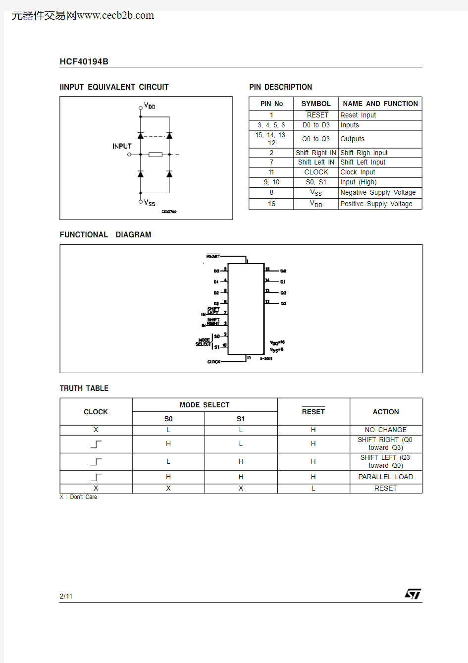
HCF40194B is a universal shift register featuring parallel inputs, parallel outputs, SHIFT RIGHT and SHIFT LEFT serial inputs, and a direct overriding clear input. In the parallel-load mode (S0 and S1are high), data is loaded into the associated flip-flop and appears at the output after the
positive transition of the CLOCK input. During loading, serial data flow is inhibited. Shift right and shift left are synchronously accomplished on the positive clock edge with data entered at the SHIFT RIGHT and SHIFT LEFT serial inputs,respectively. Clocking of the register is inhibited when both mode control inputs are low. When low,the RESET input resets all stages and forces all outputs low. HCF40194B is similar to industry types 340194 and MC40194.
HCF40194B
4-BIT BIDIRECTIONAL UNIVERSAL SHIFT REGISTER
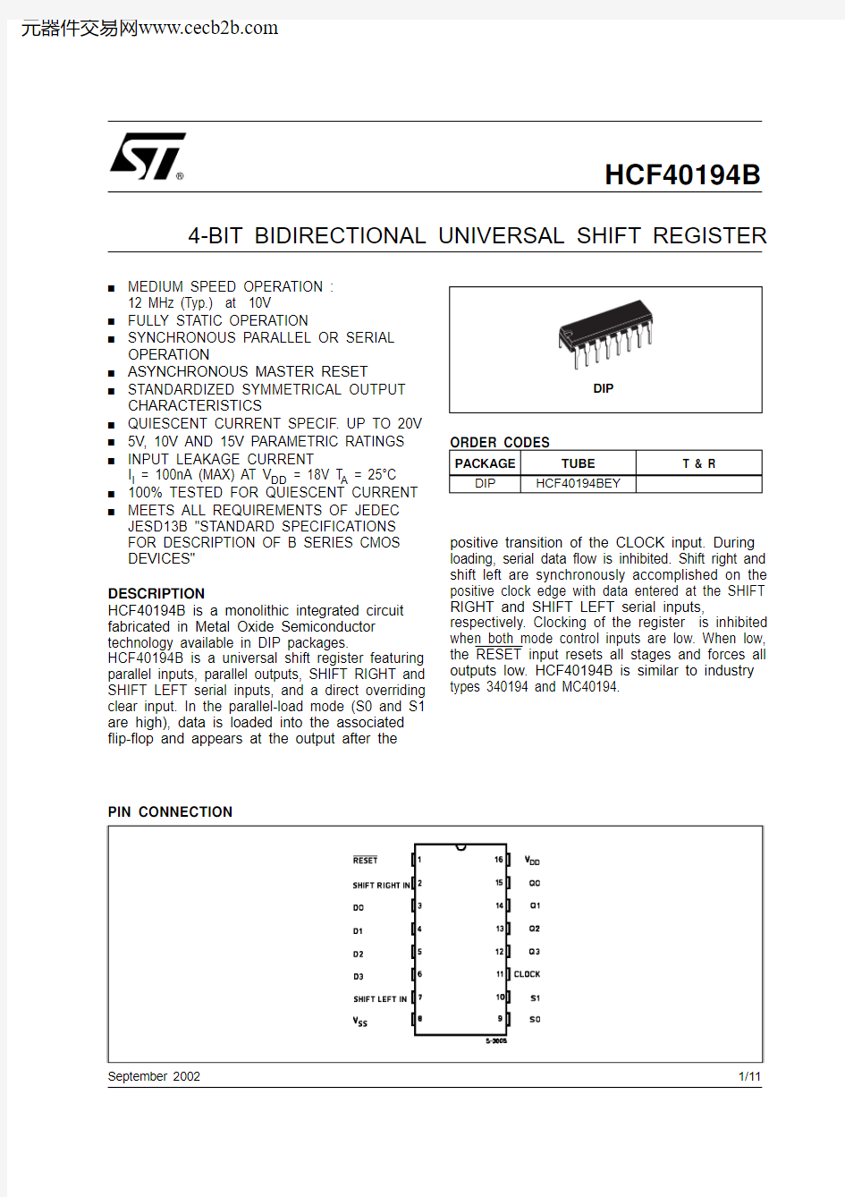
PIN CONNECTION
ORDER CODES
PACKAGE
TUBE T & R
DIP
HCF40194BEY
HCF40194B
2/11
IINPUT EQUIVALENT CIRCUIT
PIN DESCRIPTION
FUNCTIONAL DIAGRAM
TRUTH TABLE
PIN No
SYMBOL
NAME AND FUNCTION
1 RESET Reset Input 3, 4, 5, 6D0 to D3Inputs 15, 14, 13,
12Q0 to Q3Outputs
2Shift Right IN Shift Righ Input 7Shift Left IN Shift Left Input 11CLOCK Clock Input 9, 10S0, S1Input (High)
8
V SS Negative Supply Voltage 16
V DD
Positive Supply Voltage
HCF40194B LOGIC DIAGRAM
3/11
HCF40194B
4/11
ABSOLUTE MAXIMUM RATINGS
Absolute Maximum Ratings are those values beyond which damage to the device may occur. Functional operation under these conditions is not implied.
All voltage values are referred to V SS pin voltage.
RECOMMENDED OPERATING CONDITIONS
Symbol Parameter
Value Unit V DD Supply Voltage -0.5 to +22V V I DC Input Voltage -0.5 to V DD + 0.5
V I I DC Input Current
± 10mA P D Power Dissipation per Package
200mW Power Dissipation per Output Transistor 100mW T op Operating Temperature -55 to +125°C T stg
Storage Temperature
-65 to +150
°C
Symbol Parameter
Value Unit V DD Supply Voltage 3 to 20V V I Input Voltage
0 to V DD V T op
Operating Temperature
-55 to 125
°C
HCF40194B
5/11
DC SPECIFICATIONS
The Noise Margin for both "1" and "0" level is: 1V min. with V DD =5V, 2V min. with V DD =10V, 2.5V min. with V DD =15V
Symbol
Parameter
Test Condition
Value Unit
V I (V)V O (V)
|I O |(μA)V DD (V)
T A = 25°C -40 to 85°C -55 to 125°C Min.
Typ.Max.Min.
Max.Min.
Max.I L
Quiescent Current
0/550.045150150μA
0/10100.0410*******/15150.04206006000/20200.08
100
3000
3000
V OH
High Level Output Voltage
0/5<15 4.95 4.95 4.95V
0/10<1109.959.959.950/15<11514.95
14.95
14.95
V OL
Low Level Output Voltage
5/0<150.050.050.05V
10/0<1100.050.050.0515/0
<1150.050.05
0.05
V IH
High Level Input Voltage 0.5/4.5<15 3.5 3.5 3.5V
1/9<1107771.5/13.5<11511
11
11
V IL
Low Level Input Voltage 4.5/0.5<15 1.5 1.5 1.5V
9/1<11033313.5/1.5<1154
4
4
I OH
Output Drive Current
0/5 2.5<15-1.36-3.2-1.1-1.1mA
0/5 4.6<15-0.44-1-0.36-0.360/109.5<110-1.1-2.6-0.9-0.90/1513.5<115-3.0-6.8-2.4-2.4I OL
Output Sink Current
0/50.4<150.4410.360.36mA
0/100.5<110 1.1 2.60.90.90/15 1.5<1
15 3.0
6.8 2.4 2.4
I I
Input Leakage Current
0/18
Any Input 18
±10-5±0.1±1±1μA C I
Input Capacitance
Any Input
5
7.5
pF
HCF40194B
6/11
DYNAMIC ELECTRICAL CHARACTERISTICS (T amb = 25°C, C L = 50pF, R L = 200K ?, t r = t f = 20 ns)
Symbol
Parameter
Test Condition
Value (*)Unit
V DD (V)Min.
Typ.Max.t PHL t PLH Propagation Delay Time
Clock to Q 5220440ns 101002001570140t PHZ
54590ns
102550152040t THL t TLH Transition Time
5100200ns
1050100154080t setup
Setup Time D0, D3, SR, SL to Clock 580100ns
103570152050SO, S1 to Clock
5200400ns
101102201565130t hold
Hold Time D0, D3, SR, SL to Clock 5-650ns
10-25015-150SO, S1 to Clock
5-1700ns
10-95015-550t W
Clock Pulse Width
590180ns
1040180152550
f CL
Clock Input Frequency
536MHz
10612158
15
t r , t f
Clock Input Rise or Fall Time
51000μs
1010015100t W
Reset Pulse Width
5150300ns
101002001570140t PRHL
Propagation Delay Reset
5230460ns
109018015
65
130
HCF40194B
7/11
TEST CIRCUIT
C L = 50pF or equivalent (includes jig and probe capacitance)R L = 200K ?
R T = Z OUT of pulse generator (typically 50?)
WAVEFORM 1 : CK TO Q PROPAGATION DELAY TIMES
(f=1MHz; 50% duty cycle)
HCF40194B
8/11
WAVEFORM 2 : SI, SO SETUP AND HOLD TIMES (f=1MHz; 50% duty cycle)
WAVEFORM 3 : PROPAGATION DELAY TIME
(f=1MHz; 50% duty cycle)
HCF40194B WAVEFORM 4 : PROPAGATION DELAY TIME, RESET MINIMUM PULSE WIDTH (f=1MHz; 50% duty cycle)
9/11
HCF40194B Information furnished is believed to be accurate and reliable. However, STMicroelectronics assumes no responsibility for the consequences of use of such information nor for any infringement of patents or other rights of third parties which may result from its use. No license is granted by implication or otherwise under any patent or patent rights of STMicroelectronics. Specifications mentioned in this publication are subject to change without notice. This publication supersedes and replaces all information previously supplied. STMicroelectronics products are not authorized for use as critical components in life support devices or systems without express written approval of STMicroelectronics.
? The ST logo is a registered trademark of STMicroelectronics
? 2002 STMicroelectronics - Printed in Italy - All Rights Reserved
STMicroelectronics GROUP OF COMPANIES
Australia - Brazil - Canada - China - Finland - France - Germany - Hong Kong - India - Israel - Italy - Japan - Malaysia - Malta - Morocco Singapore - Spain - Sweden - Switzerland - United Kingdom - United States.
? https://www.doczj.com/doc/25202399.html,
11/11