ANPEC reserves the right to make changes to improve reliability or manufacturability without notice, and advise customers to obtain the latest version of relevant information to verify before placing orders.
APM2506NUB
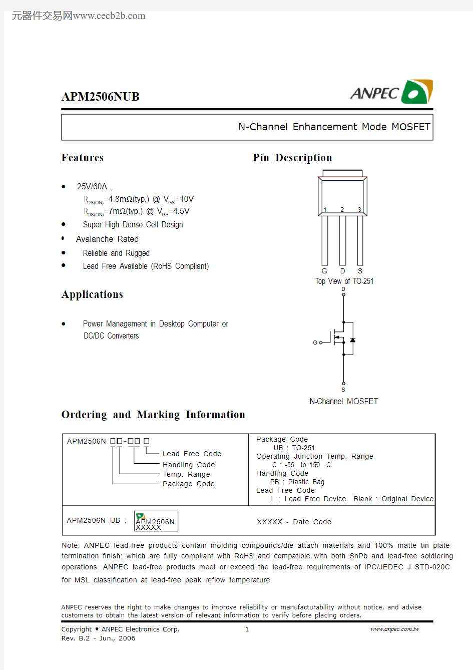
Pin Description
Ordering and Marking Information
Features
Applications
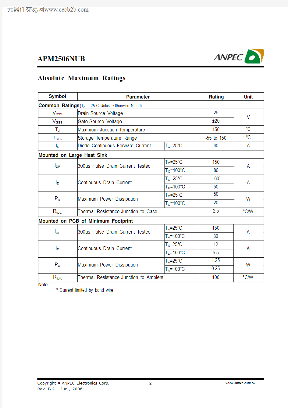
? 25V/60A ,
R DS(ON)=4.8m ?(typ.) @ V GS =10V R DS(ON)=7m ?(typ.) @ V GS =4.5V
? Super High Dense Cell Design ? Avalanche Rated ? Reliable and Rugged
? Lead Free Available (RoHS Compliant)
? Power Management in Desktop Computer or
DC/DC Converters
Note: ANPEC lead-free products contain molding compounds/die attach materials and 100% matte tin plate termination finish; which are fully compliant with RoHS and compatible with both SnPb and lead-free soldiering operations. ANPEC lead-free products meet or exceed the lead-free requirements of IPC/JEDEC J STD-020C for MSL classification at lead-free peak reflow temperature.
°APM2506N
Handling Code Temp. Range Package Code
Package Code UB : TO-251
Operating Junction Temp. Range
C : -55 to 150 C
Handling Code PB : Plastic Bag Lead Free Code
L : Lead Free Device Blank : Original Device APM2506N UB :
APM2506N XXXXX
XXXXX - Date Code
Lead Free Code Top View of TO-251
N-Channel MOSFET
G
S
123
S
D
G
APM2506NUB
Absolute Maximum Ratings
* Current limited by bond wire.
APM2506NUB
Electrical Characteristics (T
= 25°C unless otherwise noted)
A Array
Notes:
a : Pulse test ; pulse width ≤300μs, duty cycle ≤ 2%.
b : Guaranteed by design, not subject to production testing.
APM2506NUB
1E-4
1E-3
0.01
0.1
1
10
100
1E-30.01
0.1
1
2
Typical Characteristics
Power Dissipation P t o t - P o w e r (W )
T j - Junction Temperature (°C)
I D - D r a i n C u r r e n t (A )
Drain Current T j - Junction Temperature (°C)
Safe Operation Area
V DS - Drain - Source Voltage (V)
Thermal Transient Impedance Square Wave Pulse Duration (sec)
20406080100120140160180
10
20
30
40
50
60
0.1
1
1070
N o r m a l i z e d T r a n s i e
n t T h e r m a l R e s i s t a n c e 0
20406080100120140160180
10
203040506070
APM2506NUB
I D - D r a i n C u r r e n t (A )
V GS - Gate - Source Voltage (V)
T j - Junction Temperature (°C)
R D S (O N ) - O n - R e s i s t a n c e (m ?)
12345678910
APM2506NUB
Drain-Source On Resistance
N o r m a l i z e d O n R e s i s t a n c e
T j - Junction Temperature (°C)
V SD - Source-Drain Voltage (V)
Source-Drain Diode Forward
I S - S o u r c e C u r r e n t (A )
V DS - Drain - Source Voltage (V)
C - C a p a c i t a n c e (p F )
Capacitance Gate Charge
Q G - Gate Charge (nC)
V G S - G a t e -s o u r c e V o l t a g e (V )
Typical Characteristics (Cont.)
0.00
0.25
0.500.751.001.251.50
1.75
2.00
0.00.20.40.60.8 1.0 1.2 1.4
1.6
1
10
100
1000
2000
3000
40005000
0102030405060
1
23456789
10
APM2506NUB
Avalanche Test Circuit and Waveforms
Switching Time Test Circuit and Waveforms
APM2506NUB
TO-251
Packaging Information
APM2506NUB
Physical Specifications
T L
T P
25
T e m p e r a t u r e
Time
Reflow Condition (IR/Convection or VPR Reflow)
Classification Reflow Profiles
APM2506NUB
Reliability Test Program
Classification Reflow Profiles(Cont.)
Customer Service
Anpec Electronics Corp.Head Office :
No.6, Dusing 1st Road, SBIP,Hsin-Chu, Taiwan, R.O.C.Tel : 886-3-5642000Fax : 886-3-5642050Taipei Branch :
7F, No. 137, Lane 235, Pac Chiao Rd.,Hsin Tien City, Taipei Hsien, Taiwan, R. O. C.Tel : 886-2-89191368Fax : 886-2-89191369