+125O
C T
STG Symbol Typ Parameter
Conditions
Min Max Unit
Forward voltage I F = 500mA I F = 100mA V F V 0.470.36Reverse current
Capacitance between terminals
V R = 20V
f = 1 MHz, and 0 VDC reverse voltage
I R C T
uA pF
100
100
CDBK0520
Features
-Low forward voltage.
-Designed for mounting on small surface. -Extremely thin / leadless package. -Majority carrier conduction.
Mechanical data
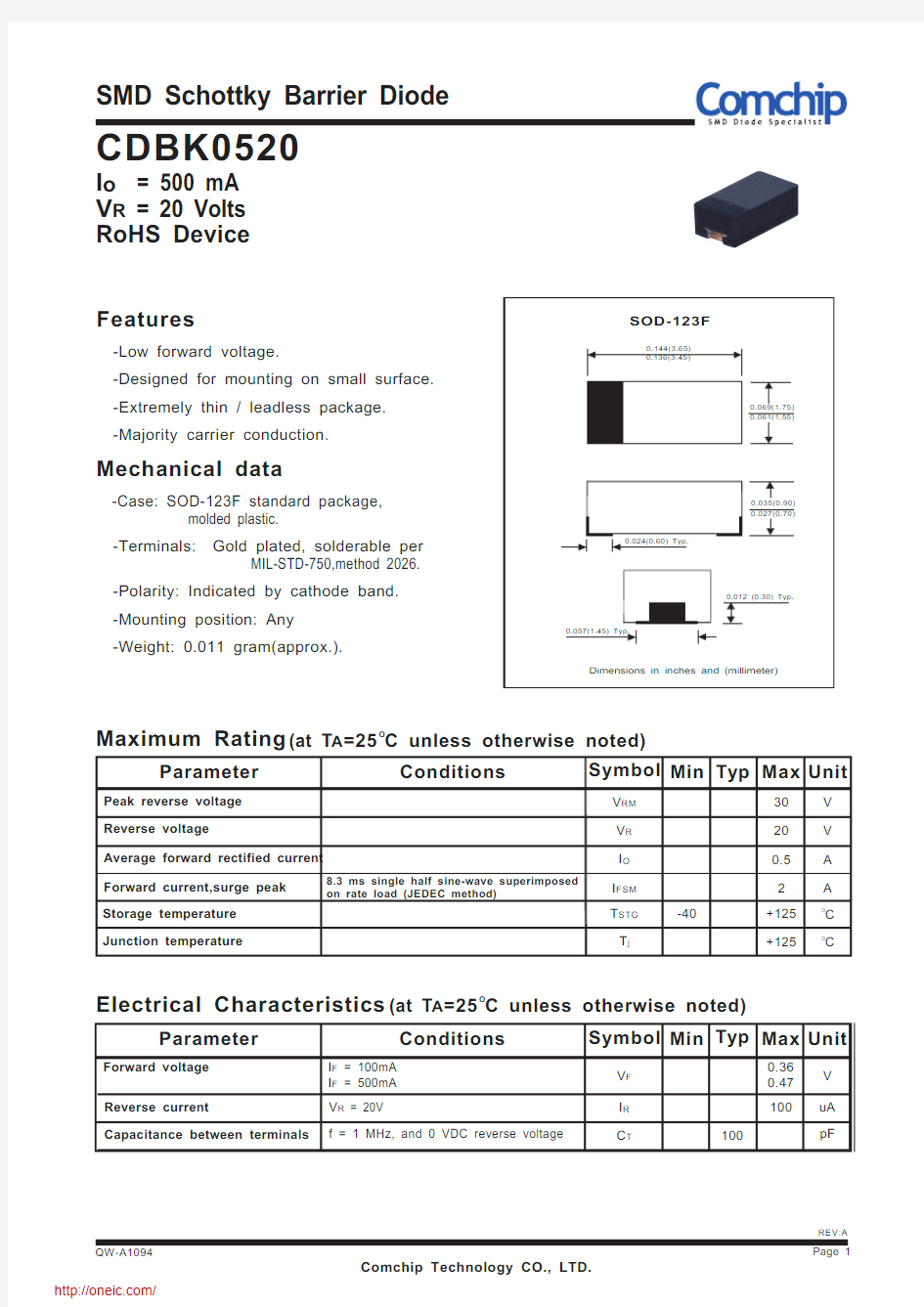
-Case: SOD-123F standard package, molded plastic.
-Terminals: Gold plated, solderable per MIL-STD-750,method 2026. -Polarity: Indicated by cathode band. -Mounting position: Any
-Weight: 0.011 gram(approx.).
O
Maximum Rating (at T A =25C unless otherwise noted)
O
Electrical Characteristics (at T A =25C unless otherwise noted)
Typ I O
V R V RM Average forward rectified current Reverse voltage
Peak reverse voltage Forward current,surge peak
Symbol Parameter
Conditions
Min Max Unit
V V A 0.52030T j
Storage temperature Junction temperature
O
C
+125
-40
I FSM 8.3 ms single half sine-wave superimposed on rate load (JEDEC method)
2
A
I o = 500 mA V R = 20 Volts RoHS Device
C a p a c i t a n c e b e t w e e n t e r m i n a l s (P F )
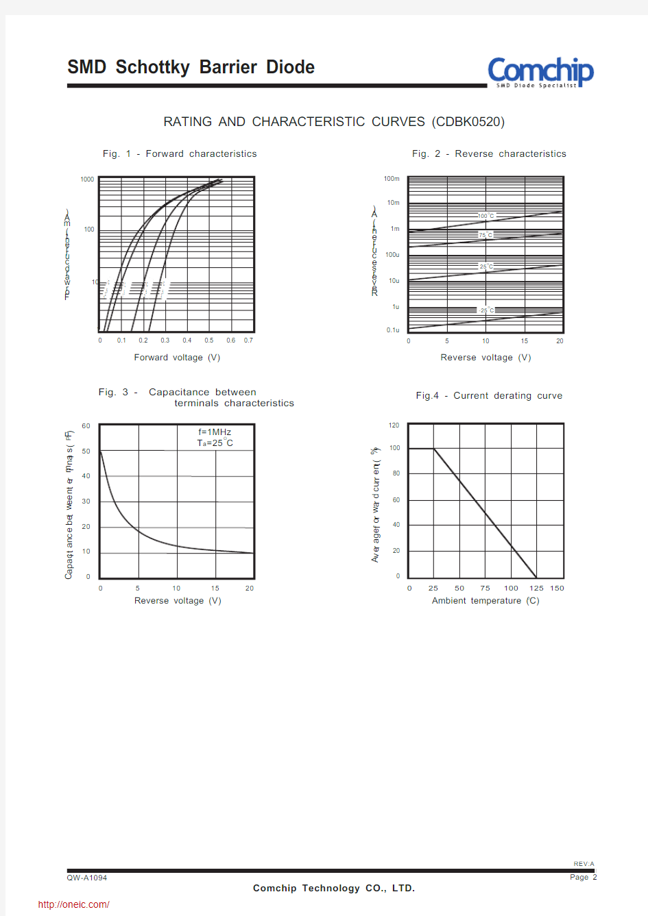
Reverse voltage (V)RATING AND CHARACTERISTIC CURVES (CDBK0520)
F o r w a r d c u r r e n t (m A )
0.2
0.4
10
1000.5
1
0.7
Forward voltage (V) Fig. 1 - Forward characteristics
R e v e r s e c u
r r e n t ( A )
Reverse voltage (V)
100u
0.1u
1m
100m 10u
1u
5
101520
Fig. 2 - Reverse characteristics
5
10
15
20
10203060f=1MHz
O
T a =25C
40500
2040
60
80
100
25
50
75
100
125150
O
Ambient temperature (C)
A v e r a g e f o r w a r d c u r r e n t (%)
Fig.4 - Current derating curve
120
1000
Fig. 3 - Capacitance between terminals characteristics
0.1
0.3
0.6
10m
分销商库存信息: COMCHIP
CDBK0520