_______________General Description
The MAX517/MAX518/MAX519 are 8-bit voltage output digital-to-analog converters (DACs) with a simple 2-wire serial interface that allows communication between multiple devices. They operate from a single 5V supply and their internal precision buffers allow the DAC out-puts to swing rail-to-rail.
The MAX517 is a single DAC and the MAX518/MAX519are dual DACs. The MAX518 uses the supply voltage as the reference for both DACs. The MAX517 has a ref-erence input for its single DAC and each of the MAX519’s two DACs has its own reference input.
The MAX517/MAX518/MAX519 feature a serial interface and internal software protocol, allowing communication at data rates up to 400kbps. The interface, combined with the double-buffered input configuration, allows the DAC registers of the dual devices to be updated indi-vidually or simultaneously. In addition, the devices can be put into a low-power shutdown mode that reduces supply current to 4μA. Power-on reset ensures the DAC outputs are at 0V when power is initially applied.
The MAX517/MAX518 are available in space-saving 8-pin DIP and SO packages. The MAX519 comes in 16-pin DIP and SO packages.
________________________Applications
Minimum Component Analog Systems Digital Offset/Gain Adjustment Industrial Process Control Automatic Test Equipment Programmable Attenuators
____________________________Features
o Single +5V Supply
o Simple 2-Wire Serial Interface o I 2C Compatible
o Output Buffer Amplifiers Swing Rail-to-Rail o
Space-Saving 8-pin DIP/SO Packages (MAX517/MAX518)
o Reference Input Range Includes Both Supply Rails (MAX517/MAX519)
o Power-On Reset Clears All Latches o 4μA Power-Down Mode
______________Ordering Information
MAX517/MAX518/MAX519
2-Wire Serial 8-Bit DACs with
Rail-to-Rail Outputs
Maxim Integrated Products 1
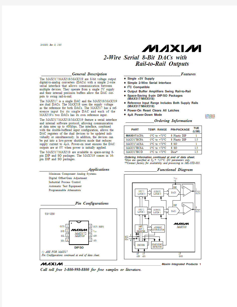
_________________Pin Configurations
________________Functional Diagram
Call toll free 1-800-998-8800 for free samples or literature.
19-0393; Rev 0; 5/95
Ordering Information continued at end of data sheet.*Dice are specified at T A = +25°C, DC parameters only.
**Contact factory for availability and processing to MIL-STD-883.
M A X 517/M A X 518/M A X 519
2-Wire Serial 8-Bit DACs with Rail-to-Rail Outputs 2_______________________________________________________________________________________
ABSOLUTE MAXIMUM RATINGS
ELECTRICAL CHARACTERISTICS
(V DD = 5V ±10%, V REF_= 4V (MAX517, MAX519), R L = 10k ?, C L = 100pF, T A = T MIN to T MAX , unless otherwise noted. Typical values are T A = +25°C.)
Stresses beyond those listed under “Absolute Maximum Ratings” may cause permanent damage to the device. These are stress ratings only, and functional operation of the device at these or any other conditions beyond those indicated in the operational sections of the specifications is not implied. Exposure to absolute maximum rating conditions for extended periods may affect device reliability.
V DD to GND..............................................................-0.3V to +6V OUT_..........................................................-0.3V to (V DD + 0.3V)REF_ (MAX517, MAX519)...........................-0.3V to (V DD + 0.3V)AD_.............................................................-0.3V to (V DD + 0.3V)SCL, SDA to GND.....................................................-0.3V to +6V Maximum Current into Any Pin............................................50mA Continuous Power Dissipation (T A = +70°C)
8-Pin Plastic DIP (derate 9.09mW/°C above +70°C)...727mW 8-Pin SO (derate 5.88mW/°C above +70°C)................471mW 8-Pin CERDIP (derate 8.00mW/°C above +70°C)........640mW
16-Pin Plastic DIP (derate 10.53mW/°C above +70°C)..842mW 16-Pin Narrow SO (derate 8.70mW/°C above +70°C)...696mW 16-Pin CERDIP (derate 10.00mW/°C above +70°C)......800mW Operating Temperature Ranges
MAX51_C_ _.......................................................0°C to +70°C MAX51_E_ _.....................................................-40°C to +85°C MAX51_MJB..................................................-55°C to +125°C Storage Temperature Range.............................-65°C to +150°C Lead Temperature (soldering, 10sec).............................+300°C
MAX517/MAX518/MAX519
2-Wire Serial 8-Bit DACs with
Rail-to-Rail Outputs
_______________________________________________________________________________________3
ELECTRICAL CHARACTERISTICS (continued)
(V DD = 5V ±10%, V REF_= 4V (MAX517, MAX519), R L = 10k ?, C L = 100pF, T A = T MIN to T MAX , unless otherwise noted. Typical values are T
= +25°C.)
M A X 517/M A X 518/M A X 519
2-Wire Serial 8-Bit DACs with Rail-to-Rail Outputs 4_______________________________________________________________________________________
DD output swing when loaded with 10k ?to GND.
Note 2:Input resistance is code dependent. The lowest input resistance occurs at code = 55 hex.Note 3:Input capacitance is code dependent. The highest input capacitance occurs at code FF hex.
Note 4:V REF_= 4Vp-p, 10kHz. Channel-to-channel isolation is measured by setting the code of one DAC to FF hex and setting the
code of all other DACs to 00 hex.
Note 5:V REF_= 4Vp-p, 10kHz, DAC code = 00 hex.Note 6:Guaranteed by design.Note 7:I 2C compatible mode.
Note 8:Output settling time is measured by taking the code from 00 hex to FF hex, and from FF hex to 00 hex.
Note 9: A master device must provide a hold time of at least 300ns for the SDA signal (referred to V IL of the SCL signal) in order to
bridge the undefined region of SCL’s falling edge.
Note 10:Cb = total capacitance of one bus line in pF. t R and t F measured between 0.3V DD and 0.7V DD .Note 11:Input filters on the SDA and SCL inputs suppress noise spikes less than 50ns.
TIMING CHARACTERISTICS
(V = 5V ±10%, T = T to T , unless otherwise noted. Typical values are T = +25°C.)
ELECTRICAL CHARACTERISTICS (continued)
(V DD = 5V ±10%, V REF_= 4V (MAX517, MAX519), R L = 10k ?, C L = 100pF, T A = T MIN to T MAX , unless otherwise noted. Typical values are T = +25°C.)
MAX517/MAX518/MAX519
2-Wire Serial 8-Bit DACs with
Rail-to-Rail Outputs
_______________________________________________________________________________________5
10
00
0.5 1.5 2.5 3.0
3.5
4.0
FULL-SCALE ERROR vs. SOURCE CURRENT
(V REF = V DD )
28
OUTPUT SOURCE CURRENT (mA)
F U L L -S C A L E E R R O R (L S B )
1.0
2.0
6
410
00
0.5
2.0
ZERO-CODE ERROR vs. SINK CURRENT
2
8
OUTPUT SINK CURRENT (mA)
Z E R O -C O D E E R R O R (L S B )
1.0
1.5
6
4
3.00
-55-155
-3565125
MAX517/MAX519 SUPPLY CURRENT
vs. TEMPERATURE
0.52.0
2.5
TEMPERATURE (°C)
S U P P L Y C U R R E N T (m A )
45
25851051.51.03.03.50
-55-35-15
5
6545125105MAX518 SUPPLY CURRENT
vs. TEMPERATURE
0.5
2.02.5TEMPERATURE (°C)S U P P L Y C U R R E N T (m A )
25851.51.060
-55-15-354565
125
SHUTDOWN SUPPLY CURRENT
vs. TEMPERATURE
145TEMPERATURE (°C)
S H U T D O W N S U P P L Y C U R R E N T (μA )
2558510532MAX518 SUPPLY CURRENT
vs. DAC CODE
DAC CODE (DECIMAL)S U P P L Y C U R R E N T (m A )
V DD = 5.5V
BOTH DACS SET
00
0.51.01.52.02.53.03264961281601922242562.5
01
0.53
2.55
4.5MAX517/MAX519 SUPPLY CURRENT
vs. REFERENCE VOLTAGE
0.51.5
2.0
REFERENCE VOLTAGE (V)
S U P P L Y C U R R E N T (m A )
2
1.54
3.51.0
1k
100k 10k
1M
10M
MAX517/MAX519 REFERENCE VOLTAGE INPUT
FREQUENCY RESPONSE
-16
FREQUENCY (Hz)
R E L A T I V E O U T P U T (d B )
-12-8
-4__________________________________________Typical Operating Characteristics
(T A = +25°C, unless otherwise noted.)
OUT0 LOADED WITH 10k ? II 100pF REF0 = 4V (MAX517/MAX519) DAC CODE = 00 HEX to FF HEX
1μs/div
POSITIVE FULL-SCALE STEP RESPONSE
OUT0 1V/div
M A X 517/M A X 518/M A X 519
2-Wire Serial 8-Bit DACs with Rail-to-Rail Outputs 6_______________________________________________________________________________________
A = REF0, 1V/div (4V P-P )
B = OUT0, 50μV/div, UNLOADED FILTER PASSBAND = 10kHz to 1MHz DA
C CODE = 00 HEX
MAX517/MAX519
REFERENCE FEEDTHROUGH AT 100kHz
B
A
______________________________T ypical Operating Characteristics (continued)
(T A = +25°C, unless otherwise noted.)
A = SCL, 400kHz, 5V/div
B = OUT0, 5mV/div DA
C CODE = 7F HEX
REF0 = 5V (MAX517/MAX519)CLOCK FEEDTHROUGH
B
A A = REF0, 1V/div (4V P-P )
B = OUT0, 50μV/div, UNLOADED FILTER PASSBAND = 100Hz to 10kHz DA
C CODE = 00 HEX
MAX517/MAX519
REFERENCE FEEDTHROUGH AT 1kHz
B
A
A = REF0, 1V/div (4V P-P )
B = OUT0, 50μV/div, UNLOADED FILTER PASSBAND = 1kHz to 100kHz DA
C CODE = 00 HEX MAX517/MAX519
REFERENCE FEEDTHROUGH AT 10kHz B
A OUT0 LOADED WITH 10k ? II 100pF REF0 = 4V (MAX517/MAX519) DAC CODE = FF HEX to 00 HEX
1μs/div
NEGATIVE FULL-SCALE STEP RESPONSE
OUT0 1V/div REF0 = 5V (MAX517/MAX519) DAC CODE = 80 HEX to 7F HEX
500ns/div
WORST-CASE 1LSB STEP CHANGE
OUT0 20mV/div AC COUPLED
MAX517/MAX518/MAX519
2-Wire Serial 8-Bit DACs with
Rail-to-Rail Outputs
7
_______________Detailed Description
Serial Interface
The MAX517/MAX518/MAX519 use a simple 2-wire serial interface requiring only two I/O lines (2-wire bus) of a standard microprocessor (μP) port. Figure 2 shows the timing diagram for signals on the 2-wire bus. Figure 3 shows a typical application. The 2-wire bus can have several devices (in addition to the MAX517/MAX518/MAX519) attached. The two bus lines (SDA and SCL) must be high when the bus is not in use. When in use, the port bits are toggled to generate the appropriate signals for SDA and SCL. External pull-up resistors are not required on these lines. The MAX517/MAX518/MAX519 can be used in applications where pull-up resis-tors are required (such as in I 2C systems) to maintain compatibility with existing circuitry.
The MAX517/MAX518/MAX519 are receive-only devices and must be controlled by a bus master device. They operate at SCL rates up to 400kHz. A master device sends information to the devices by transmitting their address over the bus and then transmitting the desired information. Each transmission consists of a START condition, the MAX517/MAX518/MAX519’s programm-able slave-address, one or more command-byte/out-put-byte pairs (or a command byte alone, if it is the last byte in the transmission), and finally, a STOP condition (Figure 4).
______________________________________________________________Pin Description
PIN
MAX517
MAX518
MAX519
NAME FUNCTION
111OUT0DAC0 Voltage Output 224GND Ground
——5AD3Address Input 3; sets IC’s slave address 336SCL Serial Clock Input 448SDA Serial Data Input
——9AD2Address Input 2; sets IC’s slave address 5510AD1Address Input 1; sets IC’s slave address 6611AD0Address Input 0; sets IC’s slave address
7712VDD Power Supply, +5V; used as reference for MAX518——13REF1Reference Voltage Input for DAC18—15REF0Reference Voltage Input for DAC0—816OUT1DAC1 Voltage Output
—
—
2, 3, 7, 14
N.C.
No Connect—not internally connected.
M A X 517/M A X 518/M A X 519
2-Wire Serial 8-Bit DACs with Rail-to-Rail Outputs
MAX517/MAX518/MAX519
2-Wire Serial 8-Bit DACs with
Rail-to-Rail Outputs
_______________________________________________________________________________________
9
these devices may share the bus. The MAX519 has 16possible slave addresses. The eighth bit (LSB) in the slave address byte should be low when writing to the MAX517/MAX518/MAX519.
The MAX517/MAX518/MAX519 monitor the bus continu-ously, waiting for a START condition followed by their slave address. When a device recognizes its slave address, it is ready to accept data.
The Command Byte and Output Byte
A command byte follows the slave address. Figure 7shows the format for the command byte. A command byte is usually followed by an output byte unless it is the last byte in the transmission. If it is the last byte, all bits except PD (power-down) and RST (reset) are
ignored. If an output byte follows the command byte,A0 of the command byte indicates the digital address of the DAC whose input data latch receives the digital output data. Set this bit to 0 when writing to the MAX517. The data is transferred to the DAC’s output latch during the STOP condition following the transmis-sion. This allows both DACs of the MAX518/MAX519 to be updated simultaneously (Figure 8).
Setting the PD bit high powers down the MAX517/MAX518/MAX519 following a STOP condition (Figure 9a). If a command byte with PD set high is followed by an output byte, the addressed DAC’s input latch will be updated and the data will be transferred to the DAC’s output latch following the STOP condition (Figure 9b).
Figure 5. All communications begin with a START condition and end with a STOP condition, both generated by a bus master.
M A X 517/M A X 518/M A X 519
2-Wire Serial 8-Bit DACs with Rail-to-Rail Outputs
10
______________________________________________________________________________________
Figure 9. Entering the Power-Down State
MAX517/MAX518/MAX519
2-Wire Serial 8-Bit DACs with
Rail-to-Rail Outputs
______________________________________________________________________________________
11
Furthermore if the transmission’s last command byte has PD high, the output latches are updated, but volt-age outputs will not reflect the newly entered data because the DAC enters power-down mode when the STOP condition is detected. When in power-down, the DAC outputs float. In this mode, the supply current is a maximum of 20μA. A command byte with the PD bit low returns the MAX517/MAX518/MAX519 to normal opera-tion following a STOP condition, with the voltage out-puts reflecting the output-latch contents (Figures 10a and 10b). Because each subsequent command byte overwrites the previous PD bit, only the last command byte of a transmission affects the power-down state.Setting the RST bit high clears the DAC input latches.The DAC outputs remain unchanged until a STOP con-dition is detected (Figure 11a). If a reset is issued, the
following output byte is ignored. Subsequent pairs of command/output bytes overwrite the input latches (Figure 11b).
All changes made during a transmission affect the MAX517/MAX518/MAX519’s outputs only when the transmission ends and a STOP has been recognized. The R0, R1, and R2 bits are reserved and must be set to zero.
I 2C Compatibility
The MAX517/MAX518/MAX519 are fully compatible with existing I 2C systems. SCL and SDA are high-impedance inputs; SDA has an open drain that pulls the data line low during the 9th clock pulse. Figure 12shows a typical I 2C application.
Figure 11. Resetting DAC Outputs
Figure 10. Returning to Normal Operation from Power-Down
M A X 517/M A X 518/M A X 519
2-Wire Serial 8-Bit DACs with Rail-to-Rail Outputs
12
______________________________________________________________________________________
It is possible to interrupt a transmission to a device with a new START (repeated start) condition (perhaps addressing another device), which leaves the input
latches with data that has not been transferred to the output latches (Figure 13). Only the currently addressed device will recognize a STOP condition and transfer data to its output latches. If the device is left with data in its input latches, the data can be transferred to the out-put latches the next time the device is addressed, as long as it receives at least one command byte and a STOP condition.
Early STOP Conditions
The addressed device recognizes a STOP condition at any point in a transmission. If the STOP occurs during a command byte, all previous uninterrupted command and output byte pairs are accepted, the interrupted command byte is ignored, and the transmission ends (Figure 14a). If the STOP occurs during an output byte,all previous uninterrupted command and output byte pairs are accepted, the final command byte ’s PD and RST bits are accepted, the interrupted output byte is ignored, and the transmission ends (Figure 14b).
Analog Section
DAC Operation
The MAX518 and MAX519 contain two matched volt-age-output DACs. The MAX517 contains a single DAC.The DACs are inverted R-2R ladder networks that con-vert 8-bit digital words into equivalent analog output voltages in proportion to the applied reference volt-ages. The MAX518 has both DAC’s reference inputs connected to V DD . Figure 15 shows a simplified dia-gram of one DAC.
MAX517/MAX519 Reference Inputs
The MAX517 and MAX519 can be used for multiplying applications. The reference accepts a 0V to V DD volt-
Figure 13. Repeated START Conditions
MAX517/MAX518/MAX519
2-Wire Serial 8-Bit DACs with
Rail-to-Rail Outputs
______________________________________________________________________________________13
age, both DC and AC signals. The voltage at each REF
input sets the full-scale output voltage for its respective DAC. The reference voltage must be positive. The DAC’s input impedance is code dependent, with the lowest value occurring when the input code is 55 hex or 0101 0101, and the maximum value occurring when the input code is 00 hex. Since the REF input resistance (RIN) is code dependent, it must be driven by a circuit with low output impedance (no more than RIN ÷2000)to maintain output linearity. The REF input capacitance is also code dependent, with the maximum value occurring at code FF hex (typically 30pF). The output voltage for any DAC can be represented by a digitally programmable voltage source as: V OUT = (N x V REF ) /256, where N is the numerical value of the DAC’s binary input code.
Output Buffer Amplifiers
The DAC voltage outputs are internally buffered preci-sion unity-gain followers that slew up to 1V/μs. The out-puts can swing from 0V to V DD . With a 0V to 4V (or 4V to 0V) output transition, the amplifier outputs typically settle to 1/2LSB in 6μs when loaded with 10k ?in paral-lel with 100pF. The buffer amplifiers are stable with any combination of resistive loads ≥2k ?and capacitive loads ≤300pF.
The MAX517/MAX518/MAX519 are designed for unipo-lar-output, single-quadrant multiplication where the out-put voltages and the reference inputs are positive with respect to AGND. Table 1 shows the unipolar code.
Table 1. Unipolar Code Table
Figure 15. DAC Simplified Circuit Diagram
Figure 14. Early STOP Conditions
DAC CONTENTS
ANALOG OUTPUT 11111111255
+ V REF (———)25610000001129+ V REF (———)25610000000128 V REF + V REF (———)= ——
256 2
01111111127
+ V REF (———)256000000011+ V REF (———)256
00000000
0V
M A X 517/M A X 518/M A X 519
2-Wire Serial 8-Bit DACs with Rail-to-Rail Outputs
MAX517/MAX518/MAX519
2-Wire Serial 8-Bit DACs with
Rail-to-Rail Outputs
______________________________________________________________________________________
15
__Ordering Information (continued)
A **Contact factory for availability and processing to MIL-STD-883.
_____Pin Configurations (continued)
TRANSISTOR COUNT: 1797
SUBSTRATE CONNECTED TO V DD
____________________Chip Topography
REF0
(MAX517/ MAX519)REF1
(MAX519)
V DD AD0
OUT0
OUT1
(MAX518/MAX519)
SDA
AD2 (MAX519)AD1 0.135" (3.429mm)
0.078" (1.981mm)
AD3 (MAX519)
SCL
GND
________________________________________________________Package Information
Maxim cannot assume responsibility for use of any circuitry other than circuitry entirely embodied in a Maxim product. No circuit patent licenses are
implied. Maxim reserves the right to change the circuitry and specifications without notice at any time.
16__________________Maxim Integrated Products, 120 San Gabriel Drive, Sunnyvale, CA 94086 (408) 737-7600?1995 Maxim Integrated Products
Printed USA
is a registered trademark of Maxim Integrated Products.
M A X 517/M A X 518/M A X 519
2-Wire Serial 8-Bit DACs with Rail-to-Rail Outputs