APDS-9900 and APDS-9901
Digital Proximity and Ambient Light Sensor
Data Sheet
Description
The APD S-9900/9901 provides digital ambient light sensing (ALS), IR LED and a complete proximity detection system in a single 8 pin package. The proximity function offers plug and play detection to 100 mm (without front glass) thus eliminating the need for factory calibration of the end equipment or sub-assembly. The proximity detection feature operates well from bright sunlight to dark rooms. The wide dynamic range also allows for operation in short distance detection behind dark glass such as a cell phone. In addition, an internal state machine provides the ability to put the device into a low power mode in between ALS and proximity measurements providing very low average power consumption. The ALS provides a photopic response to light intensity in very low light condition or behind a dark faceplate.
The APD S-9900/9901 is particularly useful for display management with the purpose of extending battery life and providing optimum viewing in diverse lighting con-ditions. D isplay panel and keyboard backlighting can account for up to 30 to 40 percent of total platform power. The ALS features are ideal for use in notebook PCs, LCD monitors, flat-panel televisions, and cell phones.
The proximity function is targeted specifically towards near field proximity applications. In cell phones, the proximity detection can detect when the user positions the phone close to their ear. The device is fast enough to provide proximity information at a high repetition rate needed when answering a phone call. This provides both improved “green” power saving capability and the added security to lock the computer when the user is not present. The addition of the micro-optics lenses within the module, provide highly efficient transmission and reception of infrared energy which lowers overall power dissipation.
Ordering Information
Part Number Packaging Quantity
APDS-9900Tape & Reel2500 per reel
APDS-9901Tape & Reel2500 per reel Features
ALS, IR LED and Proximity Detector in an Optical Module x Ambient Light Sensing (ALS)
– Approximates Human Eye Response
– Programmable Interrupt Function with Upper and Lower Threshold
– Up to 16-Bit Resolution
– High Sensitivity Operates Behind Darkened Glass
– Up to 1,000,000:1 Dynamic Range
x Proximity Detection
– Fully Calibrated to 100 mm Detection
– Integrated IR LED and Synchronous LED Driver
– Eliminates “Factory Calibration” of Prox
– Covers a 2000:1 Dynamic Range
x Programmable Wait Timer
– Wait State Power – 70 P A Typical
– Programmable from 2.72 ms to > 6 Sec
x I2C Interface Compatible
– Up to 400 kHz (I2C Fast-Mode)
– Dedicated Interrupt Pin
x Sleep Mode Power - 2.5 P A Typical
x Small Package L3.94 x W2.36 x H1.35 mm Applications
x Cell Phone Backlight Dimming
x Cell Phone Touch-screen Disable
x Notebook/Monitor Security
x Automatic Speakerphone Enable
x Automatic Menu Pop-up
x Digital Camera Eye Sensor
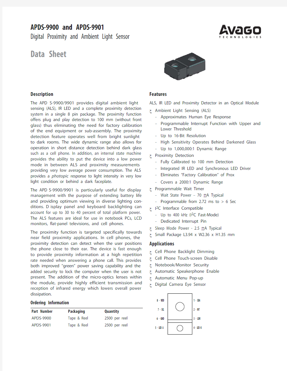
7 - SCL
6 - GND
5 - LED A
8 - VDD 1 - SDA
2 - INT
3 - LDR
4 - LED K
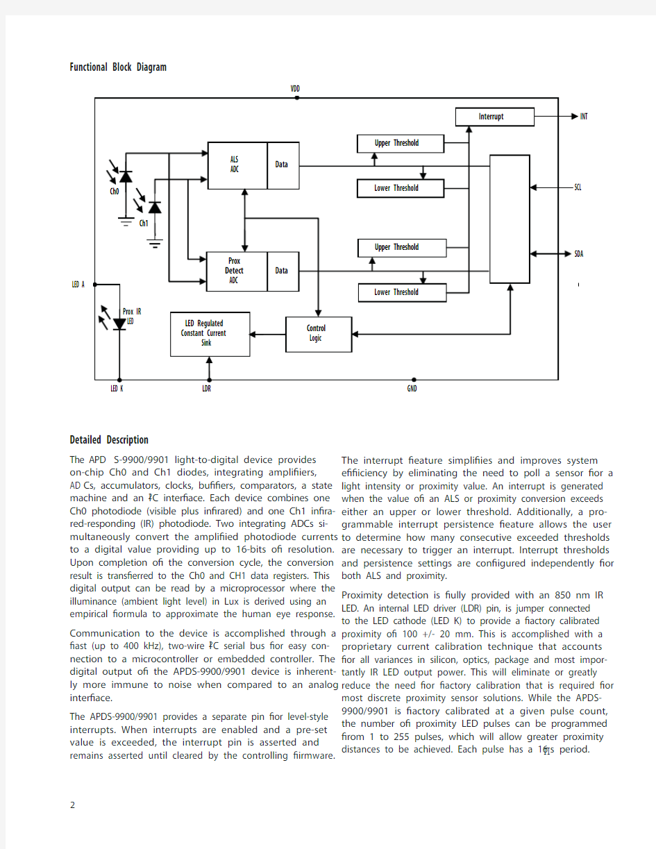
Functional Block Diagram
INT LED A
Detailed Description
The APD S-9900/9901 light-to-digital device provides on-chip Ch0 and Ch1 diodes, integrating amplifiers, AD Cs, accumulators, clocks, buffers, comparators, a state machine and an I2C interface. Each device combines one Ch0 photodiode (visible plus infrared) and one Ch1 infra-red-responding (IR) photodiode. Two integrating ADCs si-multaneously convert the amplified photodiode currents to a digital value providing up to 16-bits of resolution. Upon completion of the conversion cycle, the conversion result is transferred to the Ch0 and CH1 data registers. This digital output can be read by a microprocessor where the illuminance (ambient light level) in Lux is derived using an empirical formula to approximate the human eye response. Communication to the device is accomplished through a fast (up to 400 kHz), two-wire I2C serial bus for easy con-nection to a microcontroller or embedded controller. The digital output of the APDS-9900/9901 device is inherent-ly more immune to noise when compared to an analog interface.
The APDS-9900/9901 provides a separate pin for level-style interrupts. When interrupts are enabled and a pre-set value is exceeded, the interrupt pin is asserted and remains asserted until cleared by the controlling firmware. The interrupt feature simplifies and improves system efficiency by eliminating the need to poll a sensor for a light intensity or proximity value. An interrupt is generated when the value of an ALS or proximity conversion exceeds either an upper or lower threshold. Additionally, a pro-grammable interrupt persistence feature allows the user to determine how many consecutive exceeded thresholds are necessary to trigger an interrupt. Interrupt thresholds and persistence settings are configured independently for both ALS and proximity.
Proximity detection is fully provided with an 850 nm IR LED. An internal LED driver (LDR) pin, is jumper connected to the LED cathode (LED K) to provide a factory calibrated proximity of 100 +/- 20 mm. This is accomplished with a proprietary current calibration technique that accounts for all variances in silicon, optics, package and most impor-tantly IR LED output power. This will eliminate or greatly reduce the need for factory calibration that is required for most discrete proximity sensor solutions. While the APDS-9900/9901 is factory calibrated at a given pulse count, the number of proximity LED pulses can be programmed from 1 to 255 pulses, which will allow greater proximity distances to be achieved. Each pulse has a 16 P s period.
I/O Pins Configuration
PIN NAME TYPE DESCRIPTION
1SDA I/O I2C serial data I/O terminal – serial data I/O for I2C.
2INT O Interrupt – open drain.
3LDR I LED driver for proximity emitter – up to 100 mA, open drain.
4LEDK O LED Cathode, connect to LDR pin in most systems to use internal LED driver circuit
5LEDA I LED Anode, connect to V BATT or V DD on PCB
6GND Power supply ground. All voltages are referenced to GND.
7SCL I I2C serial clock input terminal – clock signal for I2C serial data.
8V DD Power Supply voltage.
Absolute Maximum Ratings over operating free-air temperature range (unless otherwise noted)?
Parameter Symbol Min Max Units Test Conditions
Power Supply voltage V DD 3.8V[1]
Digital voltage range-0.5 3.8V
Digital output current I O-120mA
Storage temperature range Tstg-4085°C
?Stresses beyond those listed under “absolute maximum ratings” may cause permanent damage to the device. These are stress ratings only and functional operation of the device at these or any other conditions beyond those indicated under “recommended operating conditions” is not implied. Exposure to absolute-maximum-rated conditions for extended periods may affect device reliability.
Note:
1. All voltages are with respect to GND.
Recommended Operating Conditions
Parameter Symbol Min Typ Max Units
Operating Ambient Temperature T A-3085°C
Supply voltage V DD 2.5 3.0 3.6V
-3+3%
Supply Voltage Accuracy, V DD
total error including transients
Available Options
Part Number Interface Description
APDS-9901I2C VBUS = VDD Interface
APDS-9900I2C 1.8V VBUS Interface
Operating Characteristics, V DD = 3 V, T A = 25° C (unless otherwise noted)
Parameter Symbol Min Typ Max Units Test Conditions
Supply current [1]I DD175250P A Active (ATIME=0xdb, 100ms)
60Wait Mode
2.5 4.0Sleep Mode
INT SDA output low voltage V OL00.4V 3 mA sink current
00.6 6 mA sink current Leakage current, SDA, SCL, INT Pins I LEAK-55P A
SCL, SDA input high voltage V IH0.7 V BUB
1.25V APDS-9901
APDS-9900
SCL, SDA input low voltage, V IL0.3 V BUB
0.54V APDS-9901
APDS-9900
Oscillator frequency fosc705750795kHz PON = 1
Note:
1. The power consumption is raised by the programmed amount of Proximity LED Drive during the 8 us the LED pulse is on. The nominal and
maximum values are shown under Proximity Characteristics. There the I DD supply current is I DD Active + Proximity LED Drive programmed value. ALS Characteristics, V DD = 3 V, T A = 25° C, Gain = 16, AEN = 1 (unless otherwise noted)
Parameter Channel Min Typ Max Units Test Conditions
Dark ALS ADC count value Ch0015counts Ee = 0, AGAIN = 120x,
ATIME = 0xDB(100ms)
Ch1015
ALS ADC Integration Time
Step Size
2.58 2.72 2.90ms ATIME = 0xff
ALS ADC Number of
Integration Steps
1256steps
Full Scale ADC Counts per Step1023counts
Full scale ADC count value65535counts ATIME = 0xC0
ALS ADC count value Ch0400050006000counts O p = 640 nm, Ee = 56 P W/cm2,
ATIME = 0xF6 (27 ms), GAIN = 16x
Ch1790
Ch0400050006000O p = 850 nm, Ee = 79 P W/cm2,
ATIME = 0xF6 (27 ms), GAIN = 16x
Ch12800
ALS ADC count value ratio: Ch1/Ch0 10.815.820.8%O p = 640 nm, ATIME = 0xF6 (27 ms) 415668O p = 850 nm, ATIME = 0xF6 (27 ms)
Irradiance Responsivity: Re Ch029.1Counts per
(P W/ cm2)
O p = 640 nm, ATIME = 0xF6 (27 ms) Ch1 4.6
Ch022.8O p = 850 nm, ATIME = 0xF6 (27 ms) Ch112.7
Gain scaling, relative to 1x gain setting -55%8x -5516x -55120x
Notes:
1. Optical measurements are made using small-angle incident radiation from light-emitting diode optical sources. Visible 640 nm LEDs and infrared
850 nm LEDs are used for final product testing for compatibility with high-volume production.
2. The 640 nm irradiance Ee is supplied by an AlInGaP light-emitting diode with the following characteristics: peak wavelength = 640 nm and spectral
halfwidth ? = 17 nm.
3. The 850 nm irradiance Ee is supplied by a GaAs light-emitting diode with the following characteristics: peak wavelength = 850 nm and spectral
halfwidth ? = 40 nm.
4. The specified light intensity is 100% modulated by the pulse output of the device so that during the pulse output low time, the light intensity is at
the specified level, and zero otherwise.
Proximity Characteristics, V DD = 3 V, T A = 25° C, PGAIN = 1, PEN = 1 (unless otherwise noted)
Parameter Min Typ Max Units Test Conditions
I DD Supply current – LDR Pulse On3mA
ADC Conversion Time Step Size 2.72ms PTIME = 0xff
ADC Number of Integration Steps1steps PTIME = 0xff
Full Scale ADC Counts1023counts PTIME = 0xff
Proximity IR LED Pulse Count0255pulses
Proximity Pulse Period16.3P s
Proximity Pulse – LED On Time7.2P s
Proximity LED Drive100 mA PDRIVE = 0I SINK Sink current @ 600 mV,
LDR Pin
50PDRIVE = 1
25PDRIVE = 2
12.5PDRIVE = 3
Proximity ADC count value, no object100LED driving 8 pulses, PDRIVE = 0, open view
(no glass) and no reflective object above the
module.
Proximity ADC count value, 100 mm distance object 416520624counts Reflecting object – 73 mm x 83 mm Kodak
90% grey card, 100mm distance, LED driving
8 pulses, PDRIVE = 0, open view (no glass)
above the module.
IR LED Characteristics, V DD = 3 V, T A = 25C
Parameter Min Typ Max Units Test Conditions Forward Voltage, V F 1.4 1.5V I F = 20 mA Reverse Voltage, V R 5.0V I R = 10 P A Radiant Power, P O 4.5mW I F = 20 mA Peak Wavelength, O P850nm I F = 20 mA Spectrum Width, Half Power, 'O40nm I F = 20 mA Optical Rise Time, T R20ns I FP = 100 mA Optical Fall Time, T F20ns I FP = 100 mA
Wait Characteristics, V DD = 3 V, T A = 25° C, Gain = 16, WEN = 1 (unless otherwise noted) Parameter Min Typ Max Units Test Conditions Wait Step Size 2.72ms WTIME = 0xff Wait Number of Step1256steps
Characteristics of the SDA and SCL bus lines, V DD = 3 V, T A = 25° C (unless otherwise noted)?
Parameter Symbol
STANDARD-MODE FAST-MODE
Units Min.Max.Min.Max.
SCL clock frequency f SCL01000400kHz Hold time (repeated) START condition.
After this period, the first clock pulse is generated
t HD;STA 4.0–0.6–P s
LOW period of the SCL clock t LOW 4.7– 1.3–P s HIGH period of the SCL clock t HIGH 4.0–0.6–P s Set-up time for a repeated START condition t SU;STA 4.7–0.6–P s Data hold time t HD;DAT300–300–ns Data set-up time t SU;DAT250–100–ns Rise time of both SDA and SCL signals t r–1000–300ns Fall time of both SDA and SCL signals t f–300–300ns Set-up time for STOP condition t SU;STO 4.0–0.6–P s Bus free time between a STOP and START condition t BUF 4.7– 1.3–P s Capacitive load for each bus line C b–400–400pF Noise margin at the LOW level for each connected
device (including hysteresis)
V nL0.1V BUS–0.1V BUS–V
Noise margin at the HIGH level for each connected
device (including hysteresis)
V nH0.2V BUS–0.2V BUS–V ?Specified by design and characterization; not production tested.
SDA
SCL
SCL
SDA
Figure 1. I2C Bus Timing Diagram
300
400
500
600700800900
1000
1100
W A VELE NG TH (nm)
N O R M A L I Z E D R E S P O N S I T I V I T Y
C h 0
C h 1
0.00.20.4
0.60.81.01.201000200030004000500060007000800090000
1000
2000
3000
400050006000
7000
8000
Me t er L U X
A v g S e n s o r L U X
020040060080010001200140016000
300
6009001200
1500
Me t er L U X
A v g S e n s o r L U X
0.020.040.060.080.10
0010.020.030.040.050.060.070.080.09
0.1
Me t er L U X
A v g S e n s o r L U X
0.80.9
1.0
1.1
2.4
2.6
2.8
33.2
3.4
3.6
3.8
V DD (V)
N O R M A L I Z E D I D D @ 3V 25°C
0.8
0.9
1.0
1.1
1.2
-60-40-20
020*********
TE MP E RA T UR E (°C )
N O R M A L I Z E D I D D @ 3V
1.1-100
-80-60-40
-20020406080100
ANG LE (D E G )
N O R M A L I Z E D R E S P O N S I T I V I T Y
0.00.10.20.30.40.50.60.70.80.91.0Figure 2. Spectral Response
Figure 3a. ALS Sensor LUX vs. Meter LUX using Fluorescent Light
Figure 3b. ALS Sensor LUX vs. Meter LUX using Incandescent Light Figure 3c. ALS Sensor LUX vs. Meter LUX using Low Lux Fluorescent Light
Figure 4a. Normalized IDD vs. VDD
Figure 4b. Normalized IDD vs. Temperature
Figure 5. Normalized ALS Response vs. Angular Displacement
PRINCIPLES OF OPERATION
System State Machine
The APD S-9900/9901 provides control of ALS, proximity detection and power management functionality through an internal state machine. After a power-on-reset, the device is in the sleep mode. As soon as the PON bit is set, the device will move to the start state. It will then continue through the Prox, Wait and ALS states. If these states are enabled, the device will execute each function. If the PON bit is set to a 0, the state machine will continue until all conversions are completed and then go into a low power sleep mode.
Figure 6. Simplified State Diagram
Ch0 and Ch1 Diodes
Conventional silicon detectors respond strongly to infrared light, which the human eye does not see. This can lead to significant error when the infrared content of the ambient light is high (such as with incandescent lighting) due to the difference between the silicon detector response and the brightness perceived by the human eye.
This problem is overcome in the APDS-9900/9901 through the use of two photodiodes. One of the photodiodes, referred to as the Ch0 channel, is sensitive to both visible and infrared light while the second photodiode is sensitive primarily to infrared light. Two integrating ADCs convert the photodiode currents to digital outputs. The CH1DATA digital value is used to compensate for the effect of the infrared component of light on the CH0DATA digital value. The ADC digital outputs from the two channels are used in a formula to obtain a value that approximates the human eye response in units of Lux.
ALS Operation
The ALS engine contains ALS gain control (AGAIN) and two integrating analog-to-digital converters (AD C) for the Ch0 and Ch1 photodiodes. The ALS integration time (ALSIT) impacts both the resolution and the sensitivity of the ALS reading. Integration of both channels occurs simultaneously and upon completion of the conversion cycle, the results are transferred to the Ch0 and CH1 data registers (CDATAx and IRDATAx). This data is also referred to as channel “count”. The transfers are double-buffered to ensure that invalid data is not read during the transfer. After the transfer, the device automatically moves to the next state in accordance with the configured state machine.
Figure 7. ALS Operation
NOTE: In this document, the nomenclature uses the bit field name in italics followed by the register number and bit number to allow the user to easily identify the register and bit that controls the function. For example, the power on (PON) is in register 0, bit 0. This is represented as PON (r0:b0).
The ALS Timing register value (ATIME) for programming the integration time (ALSIT) is a 2’s complement values. The ALS Timing register value can be calculated as follows:
ATIME = 256 – ALSIT / 2.72 ms
Inversely, the integration time can be calculated from the register value as follows:
ALSIT = 2.72 ms * (256 – ATIME)
For example, if a 100 ms integration time is needed, the device needs to be programmed to:
ATIME = 256 – (100 / 2.72) = 256 – 37 = 219 = 0xDB
Conversely, the programmed value of 0xC0 would correspond to:
ALSIT = (256 – 0xC0) * 2.72 =64 * 2.72 = 172 ms.
Note: 2.72 ms can be estimated as 87 / 32. Multiply by 87 the shift by 5 bits.
Calculating ALS Lux
Definition:
CH0DATA = 256 * CDATAH (r0x15) + CDATAL (r0x14)
CH1DATA = 256 * IRDATAH (r0x17) + IRDATAL (r0x16)
IAC = IR Adjusted Count
LPC = Lux per Count
ALSIT = ALS Integration Time (ms)
AGAIN = ALS Gain
DF = Device Factor, DF = 52 for APDS-9900/9901
GA = Glass (or Lens) Attenuation Factor
B, C, D – Coefficients
Lux Equation:
IAC1 = CH0DATA – B x CH1DATA
IAC2 = C x CH0DATA – D x CH1DATA
IAC = Max (IAC1, IAC2, 0)
LPC = GA x DF / (ALSIT × AGAIN)
Lux = IAC x LPC
Coefficients in open air:
GA = 0.48
B = 2.23
C = 0.7
= 1.42
Sample Lux Calculation in Open Air
Assume the following constants:
ALSIT = 400
AGAIN = 1
LPC = GA x DF / (ALSIT × AGAIN)
LPC = 0.48 x 52 / (400 x 1)
LPC = 0.06
Assume the following measurements:
CH0DATA = 5000
CH1DATA = 525
Then:
IAC1 = 5000 – 2.23 x 525 = 3829
IAC2 = 0.7 x 5000 – 1.42 x 525 = 2755
IAC = Max(3829, 2755, 0) = 3829
Lux:
Lux = IAC X LPC
Lux = 3829 X 0.06
Lux = 230
Note: please refer to application note for coefficient GA, B, C and D calculation with window.
Recommend ALS Operations
Figure 8. Attenuation vs. CH1/CH0 Ratio Figure 9. Gain and Integration Time to Lux without IR
With the programming versatility of the integration time and gain, it can be difficult to understand when to
use the different modes. Figure 8 shows a plot of the IRF
equations. Figure 9 shows a log-log plot of the Lux vs. in-tegration time and gain with a spectral factor of unity and no IR present.The maximum illuminance which can be measured is ~10k Lux with no IR present. The intercept with a count of 1 shows the resolution of each setting. The Lux values in the table increase as the SF increases (spectral attenu-ation increases). For example, if a 10% transmissive glass
is used, the Lux values would all be multiplied by 10. The
Lux values in the table decrease as the IR Factor decreases.
For example, with a 10% IR Factor, which corresponds to a strong incandescent light, the Lux value would need to be divided by 10.
There are many factors that will impact the decision on which value to use for integration time and gain. One of the first factors is 50/60 Hz ripple rejection for fluorescent lighting. The programmed value needs to be multiples of 10/8.3 ms or the half cycle time. Both frequencies can be rejected with a programmed value of 50 ms (ATIME = 0xED). With this value, the resolution will be 1.3 Lux per count. If higher resolution is needed, a longer integration time may be needed. In this case, the integration time should be programmed in multiples of 50.
The light level is the next determining factor for config-uring device settings. Under bright conditions, the count will be fairly high. If a low light measurement is needed, a higher gain and/or longer integration time will be needed. As a general rule, it is recommended to have a Ch0 channel count of at least 10 to accurately apply the Lux equation. The digital accumulation is limited to 16 bits, which occurs at an integration time of 173 ms. This is the maximum recommended programmed integration time before increasing the gain. (150 ms is the maximum to reduce the fluorescent ripple.)
Proximity Detection
Proximity sensing uses an internal IR LED light source to
emit light which is then viewed by the integrated light detector to measure the amount of reflected light when an object is in the light path. The amount of light detected from a reflected surface can then be used to determine an object’s proximity to the sensor. The APDS-9900/9901 is factory calibrated to meet the requirement of proximity sensing of 100+/- 20 mm, thus eliminating the need for factory calibration of the end equipment. When the APDS-9900/9901 is placed behind a typical glass surface, the proximity detection achieved is around 25 to 40 mm, thus providing an ideal touch-screen disable.
The APD S-9900/9901 has controls for the number of IR pulses (PPCOUNT), the integration time (PTIME), the LED drive current (PDRIVE) and the photodiode configuration (PDIODE). At the end of the integration cycle, the results are latched into the proximity data (PDATA) register.
The LED drive current is controlled by a regulated current sink on the LDR pin. This feature eliminates the need to use
a current limiting resistor to control LED current. The LED drive current can be configured for 12.5 mA, 25 mA, 50 mA,
or 100 mA. For higher LED drive requirements, an external
P type transistor can be used to control the LED current. The number of LED pulses can be programmed to a value of 1 to 255 pulses as needed. Increasing the number of LED pulses at a given current will increase the sensor sen-sitivity. Sensitivity grows by the square root of the number of pulses. Each pulse has a 16 P S period.The proximity integration time (PTIME) is the period of
time that the internal AD C converts the analog signal
to a digital count. It is recommend that this be set to a minimum of PTIME = 0xFF or 2.72 ms. Figure 10. Proximity IR LED Waveform
IRLED Pulses
Subtract Background Add IR +Background
10.90.80.70.60.50.40.30.20.10
C H1/C H 0 Ra t io
I R F a c t o r
0.01
0.1110100100010000Co unt s
L U X
Optical Design Considerations
The APDS-9900/9901 simplifies the optical system design by eliminating the need for light pipes and improves system optical efficiency by providing apertures and package shielding which will reduce crosstalk when placed in the final system. By reducing the IR LED to glass surface crosstalk, proximity performance is greatly improved and enables a wide range of cell phone applications utilizing the APD S-9900/9901. The module package design has been optimized for minimum package foot print and short distance proximity of 100 mm typical. The spacing between the glass surface and package top surface is critical to controlling the crosstalk. If the package to top surface spacing gap, window thickness and transmittance are met, there should be no need to add additional com-ponents (such as a barrier) between the LED and photo-diode. Thus with some simple mechanical design imple-mentations, the APDS-9900/9901 will perform well in the end equipment system.
APDS-9900/9901 Module Optimized design parameters x Window thickness, t ≤ 1.0 mm x Air gap, g ≤ 0.5 mm
x Assuming window IR transmittance 90%
The APDS-9900/9901 is available in a low profile package that contains optics which provides optical gain on botht the LED and the sensor side of the package. The device has a package Z height of 1.35 mm and will support air gap of < = 0.5 mm between the glass and the package. The assumption of the optical system level design is that glass surface above the module is < = to 1.0 mm.
By integrating the micro-optics in the package, the IR energy emitted can be reduced thus conserving the precious battery life in the application.
The system designer has the ability to optimize their designs for slim form factor Z height as well as improve the proximity sensing, save battery power and disable the touch screen in a cellular phone.
g
P l as t ic /G l ass W i n dow
W i n dows Th ic kn ess, t
Figure 11. Proximity Detection
Figure 12a. PS Output vs. Distance, at Various Pulse number (LED drive Current). No glass in front of the module, 18% Kodak Grey Card.Figure 12b. PS Output vs. Distance, at Various Pulse number (LED drive Current). No glass in front of the module, 90% Kodak Grey Card.
11P S C O U N T
D I S T ANC
E (c m)
11P S C O U N T D I S T ANC E (c m)
Interrupts
The interrupt feature of the APD S-9900/9901 simplifies and improves system efficiency by eliminating the need to poll the sensor for a light intensity or proximity value. The interrupt mode is determined by the PIEN or AIEN field in the ENABLE register.
The AP
S-9900/9901 implements four 16-bit-wide interrupt threshold registers that allow the user to define thresholds above and below a desired light level. For
ALS, an interrupt can be generated when the ALS Ch0 data (CDATA) exceeds the upper threshold value (AIHTx) or falls below the lower threshold (AILTx). For proximity, an interrupt can be generated when the proximity data (PDATA) exceeds the upper threshold value (PIHTx) or falls below the lower threshold (PILTx).
To further control when an interrupt occurs, the APD S-9900/9901 provides an interrupt persistence feature. This
feature allows the user to specify a number of conversion cycles for which an event exceeding the ALS interrupt threshold must persist (APERS) or the proximity interrupt threshold must persist (PPERS) before actually generating an interrupt. Refer to the register descriptions for details on the length of the persistence.
Figure 13. Programmable Interrupt
State Diagram
The following shows a more detailed flow for the state machine. The device starts in the sleep mode. The PON bit is written to enable the device. If the PEN bit is set, the state machine will step through the proximity states of proximity accumulate and then proximity AD C con-version. As soon as the conversion is complete, the state machine will move to the following state.
If the WEN bit is set, the state machine will then cycle through the wait state. If the WLONG bit is set, the wait cycles are extended by 12x over normal operation. When the wait counter terminates, the state machine will step to the ALS state.
When AEN bit is set, the state machine will step through the ALS states of ALS accumulate and then ALS ADC con-version. In this case, a minimum of 1 integration time step should be programmed. The ALS state machine will continue until it reaches the terminal count at which point the data will be latched in the ALS register and the interrupt set, if enabled.
Power Management
Power consumption can be controlled through the use of the wait state timing since the wait state consumes only 60 P A of power. The following shows an example of using the power management feature to achieve an average power consumption of 153 P A of current with 4 – 100 mA pulses of proximity detection and 50 ms of ALS detection.
Figure 14. Extended State Diagram
Ti m Maxi Ti m Reco
Step: 2.72 m s
Ti m e: 2.72 m s – 696 m s Mini m u m – 2.72 m s
Step: 32.64 m s
Ti m e: 32.64 m s – 8.35 s Mini m u m – 32.64 m s
s
Figure 15. Power Consumption Calculations Avg = ((0.032 x 100) + (2.72 x 0.175) + (47 x 0.060) + (50 x 0.175)) ÷ 100 = 153 M A
Exa m ple: 100 m s Cycle Ti m e State Duration (m s) Current (m A) Prox ADC WAIT ALS 2.7247500.1750.0600.175
Basic Software Operation
The following pseudo-code shows how to do basic initialization of the APDS-9900/9901.
uint8 ATIME, PIME, WTIME, PPCOUNT;
ATIME = 0xff; // 2.7 ms – minimum ALS integration time
WTIME = 0xff; // 2.7 ms – minimum Wait time
PTIME = 0xff; // 2.7 ms – minimum Prox integration time
PPCOUNT = 1; // Minimum prox pulse count
WriteRegData(0, 0); //Disable and Powerdown
WriteRegData (1, ATIME);
WriteRegData (2, PTIME);
WriteRegData (3, WTIME);
WriteRegData (0xe, PPCOUNT);
uint8 PDRIVE, PDIODE, PGAIN, AGAIN;
PDRIVE = 0; //100mA of LED Power
PDIODE = 0x20; // CH1 Diode
PGAIN = 0; //1x Prox gain
AGAIN = 0; //1x ALS gain
WriteRegData (0xf, PDRIVE | PDIODE | PGAIN | AGAIN);
uint8 WEN, PEN, AEN, PON;
WEN = 8; // Enable Wait
PEN = 4; // Enable Prox
AEN = 2; // Enable ALS
PON = 1; // Enable Power On
WriteRegData (0, WEN | PEN | AEN | PON); // WriteRegData(0,0x0f);
Wait(12); //Wait for 12 ms
int CH0_data, CH1_data, Prox_data;
CH0_data = Read_Word(0x14);
CH1_data = Read_Word(0x16);
Prox_data = Read_Word(0x18);
WriteRegData(uint8 reg, uint8 data)
{
m_I2CBus.WriteI2C(0x39, 0x80 | reg, 1, &data);
}
uint16 Read_Word(uint8 reg);
{
uint8 barr[2];
m_I2CBus.ReadI2C(0x39, 0xA0 | reg, 2, ref barr);
return (uint16)(barr[0] + 256 * barr[1]);
}
I 2C Protocol
Interface and control of the APD S-9900/9901 is ac-complished through an I 2C serial compatible interface (standard or fast mode) to a set of registers that provide access to device control functions and output data. The device supports a single slave address of 0x39 hex using 7 bit addressing protocol. (Contact factory for other ad-dressing options.)
The I 2C standard provides for three types of bus trans-action: read, write and a combined protocol. D uring a write operation, the first byte written is a command byte followed by data. In a combined protocol, the first byte
written is the command byte followed by reading a series of bytes. If a read command is issued, the register address from the previous command will be used for data access. Likewise, if the MSB of the command is not set, the device will write a series of bytes at the address stored in the last valid command with a register address. The command byte contains either control information or a 5 bit register address. The control commands can also be used to clear interrupts. For a complete description of I 2C protocols, please review the I 2C Specification at: http://www.NXP .com
Start and Stop conditions
SCL
SDA
START condition
STOP condition
Data transfer on I 2C-bus
SCL
repeated START condition
byte co m plete,interrupt within slave clock line held LOW while interrupts are serviced
repeated START condition
A complete data transfer
condition condition
MBC604
A Acknowledge (0)N Not Acknowledged (1)P Stop Condition R Read (1)S Start Condition Sr Repeated Start Condition W Write (0)
Continuation of protocol
17118
11711811I 2
C Read Protocol – Combined Format
17118
1811I 2
C Write Protocol
I
C Write Protocol (Clear Interrupt)
17118
181811I 2
C Write Word Protocol
17118
1171181
I 2C Read Word Protocol
Register Set
The APDS-9900/9901 is controlled and monitored by data registers and a command register accessed through the serial interface. These registers provide for a variety of control functions and can be read to determine results of the ADC conversions.
ADDRESS RESISTER NAME R/W REGISTER FUNCTION Reset Value
?COMMAND W Specifies register address0x00
0x00ENABLE R/W Enable of states and interrupts 0x00
0x01ATIME R/W ALS ADC time0x00
0x02PTIME R/W Proximity ADC time0xFF
0x03WTIME R/W Wait time0xFF
0x04AILTL R/W ALS interrupt low threshold low byte0x00
0x05AILTH R/W ALS interrupt low threshold hi byte0x00
0x06AIHTL R/W ALS interrupt hi threshold low byte0x00
0x07AIHTL R/W ALS interrupt hi threshold hi byte0x00
0x08PILTL R/W Proximity interrupt low threshold low byte0x00
0x09PILTH R/W Proximity interrupt low threshold hi byte0x00
0x0A PIHTL R/W Proximity interrupt hi threshold low byte0x00
0x0B PIHTH R/W Proximity interrupt hi threshold hi byte0x00
0x0C PERS R/W Interrupt persistence filters0x00
0x0D CONFIG R/W Configuration0x00
0x0E PPCOUNT R/W Proximity pulse count0x00
0x0F CONTROL R/W Gain control register0x00
0x11REV R Revision Number Rev
0x12ID R Device ID ID
0x13STATUS R Device status0x00
0x14CDATAL R Ch0 ADC low data register0x00
0x15CDATAH R Ch0 ADC high data register0x00
0x16IRDATAL R Ch1 ADC low data register0x00
0x17IRDATAH R Ch1 ADC high data register0x00
0x18PDATAL R Proximity ADC low data register0x00
0x19PDATAH R Proximity ADC high data register0x00
The mechanics of accessing a specific register depends on the specific protocol used. See the section on I2C protocols on the previous pages. In general, the COMMAND register is written first to specify the specific control/status register for following read/write operations.
Command Register
The command registers specifies the address of the target register for future write and read operations.
FIELD BITS DESCRIPTION
COMMAND7Select Command Register. Must write as 1 when addressing COMMAND register.
TYPE6:5Selects type of transaction to follow in subsequent data transfers:
FIELD VALUE INTEGRATION TIME
00Repeated Byte protocol transaction
01Auto-Increment protocol transaction
10Reserved – Do not use
11Special function – See description below
Byte protocol will repeatedly read the same register with each data access.
Block protocol will provide auto-increment function to read successive bytes.
ADD4:0Address register/special function register. Depending on the transaction type, see above, this field
either specifies a special function command or selects the specific control-status-register for
following write or read transactions:
FIELD VALUE READ VALUE
00000Normal – no action
00101Proximity interrupt clear
00110ALS interrupt clear
00111Proximity and ALS interrupt clear
other Reserved – Do not write
ALS/Proximity Interrupt Clear. Clears any pending ALS/Proximity interrupt. This special function is
self clearing.
Enable Register (0x00)
The ENABLE register is used primarily to power the APDS-9900/9901 device up and down as shown in Table 4.
FIELD BITS DESCRIPTION
Reserved7:6Reserved. Write as 0.
PIEN5Proximity Interrupt Enable. When asserted, permits proximity interrupts to be generated.
AIEN4ALS Interrupt Enable. When asserted, permits ALS interrupt to be generated.
WEN3Wait Enable. This bit activates the wait feature. Writing a 1 activates the wait timer.
Writing a 0 disables the wait timer.
PEN2Proximity Enable. This bit activates the proximity function. Writing a 1 enables proximity.
Writing a 0 disables proximity.
AEN1ALS Enable. This bit actives the two channel ADC. Writing a 1 activates the ADC.
Writing a 0 disables the ADC.
PON0Power ON. This bit activates the internal oscillator to permit the timers and ADC channels to operate.
Writing a 1 activates the oscillator. Writing a 0 disables the oscillator.
Notes:
1. A
2.72 ms delay is automatically inserted prior to entering the ADC cycle, independent of the WEN bit.
2. Both AEN and PON must be asserted before the ADC channels will operate correctly.
3. During writes and reads over the I2C interface, this bit is overridden and the oscillator is enabled, independent of the state of PON.
4. A minimum interval of 2.72 ms must pass after PON is asserted before either proximity or an ALS can be initiated. This required time is enforced by
the hardware in cases where the firmware does not provide it.
ALS Timing Register (0x01)
The ALS timing register controls the integration time of the ALS Ch0 and Ch1 channel ADCs in 2.72 ms increments. FIELD BITS DESCRIPTION
ATIME7:0VALUE CYCLES TIME (ALSIT)Max Count
0xff1 2.72 ms1023
0xf61027.2 ms10239
0xdb37100.64 ms37887
0xc064176.8 ms65535
0x00256696.32 ms65535
Proximity Time Control Register (0x02)
The proximity timing register controls the integration time of the proximity ADC in 2.72 ms increments. It is recommended that this register be programmed to a value of 0xff (1 cycle, 1023 bits).
FIELD BITS DESCRIPTION
Count
PTIME7:0VALUE CYCLES TIME Max 0xff1 2.72 ms1023
Wait Time Register (0x03)
Wait time is set 2.72 ms increments unless the WLONG bit is asserted in which case the wait times are 12x longer. WTIME is programmed as a 2’s complement number.
FIELD BITS DESCRIPTION
WTIME7:0REGISTER VALUE WALL TIME TIME (WLONG = 0) TIME (WLONG = 1)
0xff1 2.72 ms0.032 sec
0xb674201.29 ms 2.37 sec
0x00256696.32 ms8.19 sec
Notes:
1. The Write Byte protocol cannot be used when WTIME is greater than 127.
2. The Proximity Wait Time Register should be configured before PEN and/or AEN is/are asserted.
ALS Interrupt Threshold Register (0x04 ? 0x07)
The ALS interrupt threshold registers provides the values to be used as the high and low trigger points for the com-parison function for interrupt generation. If the value generated by the ALS channel crosses below the low threshold specified, or above the higher threshold, an interrupt is asserted on the interrupt pin.
REGISTER ADDRESS BITS DESCRIPTION
AILTL0x047:0ALS Ch0 channel low threshold lower byte
AILTH0x057:0ALS Ch0 channel low threshold upper byte
AIHTL0x067:0ALS Ch0 channel high threshold lower byte
AIHTH0x077:0ALS Ch0 channel high threshold upper byte
Note: The Write Word protocol should be used to write byte-paired registers.
Proximity Interrupt Threshold Register (0x08 ? 0x0B)
The proximity interrupt threshold registers provide the values to be used as the high and low trigger points for the com-parison function for interrupt generation. If the value generated by proximity channel crosses below the lower threshold specified, or above the higher threshold, an interrupt is signaled to the host processor.
REGISTER ADDRESS BITS DESCRIPTION
PILTL0x087:0Proximity ADC channel low threshold lower byte
PILTH0x097:0Proximity ADC channel low threshold upper byte
PIHTL0x0A7:0Proximity ADC channel high threshold lower byte
PIHTH0x0B7:0Proximity ADC channel high threshold upper byte
Persistence Register (0x0C)
The persistence register controls the filtering interrupt capabilities of the device. Configurable filtering is provided to allow interrupts to be generated after each ADC integration cycle or if the ADC integration has produced a result that is outside of the values specified by threshold register for some specified amount of time. Separate filtering is provided for proximity and ALS functions.
ALS interrupts are generated by looking only at the ADC integration results of channel 0.
FIELD BITS DESCRIPTION
PPERS7:4Proximity interrupt persistence. Controls rate of proximity interrupt to the host processor.
FIELD VALUE MEANING INTERRUPT PERSISTENCE FUNCTION
0000Every Every proximity cycle generates an interrupt
00011 1 consecutive proximity values out of range
………
11111515 consecutive proximity values out of range
APERS3:0Interrupt persistence. Controls rate of interrupt to the host processor.
FIELD VALUE MEANING INTERRUPT PERSISTENCE FUNCTION
0000Every Every ALS cycle generates an interrupt
00011 1 consecutive Ch0 channel values out of range
00102 2 consecutive Ch0 channel values out of range
00113 3 consecutive Ch0 channel values out of range
01005 5 consecutive Ch0 channel values out of range
01011010 consecutive Ch0 channel values out of range
01101515 consecutive Ch0 channel values out of range
01112020 consecutive Ch0 channel values out of range
10002525 consecutive Ch0 channel values out of range
10013030 consecutive Ch0 channel values out of range
10103535 consecutive Ch0 channel values out of range
10114040 consecutive Ch0 channel values out of range
11004545 consecutive Ch0 channel values out of range
11015050 consecutive Ch0 channel values out of range
11105555 consecutive Ch0 channel values out of range
11116060 consecutive Ch0 channel values out of range
MySQL 数据库常用命令简单超级实用版 1、MySQL常用命令 create database name; 创建数据库 use databasename; 选择数据库 drop database name 直接删除数据库,不提醒 show tables; 显示表 describe tablename; 表的详细描述 select 中加上distinct去除重复字段 mysqladmin drop databasename 删除数据库前,有提示。 显示当前mysql版本和当前日期 select version(),current_date; 2、修改mysql中root的密码: shell>mysql -u root -p mysql> update user set password=password(”xueok654123″) where user='root'; mysql> flush privileges //刷新数据库 mysql>use dbname;打开数据库: mysql>show databases; 显示所有数据库 mysql>show tables; 显示数据库mysql中所有的表:先use mysql;然后 mysql>describe user; 显示表mysql数据库中user表的列信息); 3、grant 创建一个可以从任何地方连接服务器的一个完全的超级用户,但是必须使用一个口令some thing做这个 mysql> grant all privileges on *.* to user@localhost identified by 'something' with 增加新用户
一、文件夹篇 All Users 这里记录的是Window的用户以及这些用户个人设定的开始菜单及桌面等信息。 Command 在这个目录下有着许多的DOS的常用命令,例如debug,format 等。可别小看这些老廉颇呀,在许多关键时刻还得靠他们哟。 Config 用于存放Windows中硬件配制文件。 Cursors 这是存放Windows光标的目录。 Desktop 除了"我的电脑"、"我的文档"这几个系统图标外其它由程序和文档建立的桌面快捷方式都会在这里面找到。如果在这里删除某个图标,相应的就会删除桌面上的图标。如果你在桌面上存放文件的话,实际也就是存放在这个文件夹。 Downloaded Program Files 该目录存放上网下载东东时的临时文件。 Favorites 存放收藏夹的内容。
Fonts 这是存放Windows的字体文件的目录。要安装某种字体只需将字体文件直接复制到该目录下即可。 Help 存放Windows帮助文件。 History 默认状态时可以保留你近二十天来的IE 操作记录。 Media 这里存放着Windows系统的声音文件,像Windows启动结束时发出的微软招牌音乐Microsoft Sound等都存放于此。 Offline Web Pages 这里存放着用于离线浏览的文件。 Recent 这是对应开始菜单中文档菜单下的文档调用历史记录。它会把你最近打开的文档和图片的路径记录下来,方便用户快速打开最近使用的文档。 SendTo 这个目录对应的是对文件使用"发送到"命令时的"目的地"。你可以在里面为常用的文件夹添
加快捷方式,以后再复制文件时就不必抓着鼠标到处找了。 Start Menu 对应Windows的开始菜单,可以直接在改目录对开始菜单进行管理。 Start Menu/Programs 开始菜单的程序。 Start Menu/Programs/启动自动运行。 INF INF驱动程序脚本文件夹。 OTHER INF其它驱动程序脚本文件夹。 Wallpaper 网页背景文件夹。 SYSBCKUP 系统文件备份文件夹。 System和System32 这是两个很重要的系统文件夹,存放Windows的系统文件和硬件驱动程序等重要信息。
常用调试说明 报警主机的编程并不是很复杂。在编程之前,敬请用户必须先详细地阅读安装使用说明书,(再次敬请用户认真阅读使用说明书!可达到事半功倍的效果!)并清楚的知道你所需要的功能,根据所需列出编程表,这样方便于编程。 编程前请认真阅读说明书,正确的接好连线。(正确接好连线是编好程序的前提)。如果是第一次使用DS7400主机,在编程完成前,建议安装技术人员不要将探测器接入主机,只需要将线尾电阻和扩展模块接在主机上就可以,将主机调试好后,在将探测器接入防区,这样如果系统有故障,有利于工程技术人员判断是主机系统故障还是探测器故障。 1. 正常布防:密码(1234)+“布防”键。 2. 撤防和消警:密码(1234)+“撤防”键。 3. 强制布防:密码(1234)+“布防”键+“旁路”键 4. 防区旁路:密码(1234)+“旁路”键+XXX(防区号,且一定是三位数,如008) 5. 进入编程和退出编程:进入编程是9876#0(密码+#0),退出编程是按“*”四秒钟, 听到“嘀”一声表示已退出编程。 6. 如何填写数据:DS7400主机的编程地址一定是四位数,地址的数据一定是两位数。进 入编程后,键盘的灯都会闪动,LCD显示:Prog Mode 4.05 Adr=DS7400 Adr=后面的就是要写上去的四位数的地址。输入地址后,接着输入21# 则会交替显示该地址上的两位数据;或者按“#”则可以出现数据1;再按“#”则可出现数据2。(出厂值,可以通过编程改变的),然后自动跳到下一个地址。如果需要对某些地址编程,则需连续按两次“*”则可以回到Prog Mode 4.05 Adr= 7. 确定防区的功能:(地址是0001—0030),所谓防区功能就是该防区是延时防区、即 时防区、24小时防区等等。其中01代表延时防区;03代表即时防区;07代表24小时防区。(此项一般不用编写,用出厂值即可) 8. 确定一个防区的功能:(地址是0031—0278),0031代表第一防区,0032代表第二 防区,如此类推………如果想把第八防区设定为即时防区,即可以把地址0038中的数据改为03 ,再按“#”确认就可以了。(注意:此项一定要编写) 9. 防区特性的设置:(地址是0415—0538),0415代表第一、二防区,0416代表第三、 四防区,如此类推………。数据1代表前面一个防区,数据二代表后面的一个防区。 此类表示防区使用那种扩充模块。如果使用的防区是主机自带防区和DS-7457I的扩充防区则需把数据设定为0 ;如果使用的防区是DS-7432的扩充防区则需把数据设定为1。 10. 分区编程:DS7400可分8个分区,并可以自由设定每个分区包含那些防区。 11. DS7400把系统分区:(地址是3420),其中数据1表示使用多少个分区,输入0代 表1个分区;输入1代表2个分区……….输入7代表8个分区。出厂值是0;数据2表示有无公共分区,出厂值是0。(如果系统不分区,此项不用编程) 12. DS7400确定防区属于那些分区:(地址是0287—0410),0287代表第一、二防区, 0288代表第三、四防区,如此类推………。数据1代表前面一个防区,数据二代表后面的一个防区。数据1、2可以设定为0—7,代表着1分区到8分区。(如果系统不分区,此项不用编程) 13. DS7400键盘的分区管理:DS7400主机可以支持15个键盘,1个键盘可以管理1个 分区,但每个分区可以由1个或几个键盘来管理。地址(3131—3138)代表着键盘号,3131代表第一、二号键盘,3132代表第三、四号键盘,如此类推………。数据1、2表示键盘的功能。0表示不使用;1表示LCD键盘;2表示LED键盘;3表示LCD键盘并为主键盘。(如果系统不分区,此项不用编程)
oracle常用命令 命令解释 $Ps –ef|grep oracle 查看oracle进程是否启动 $ sqlplus "/as sysdba" 以sysdba角色登陆oracle数据库 SQL>startup 显示当前系统中已登录的人员。 SQL>shutdown immediate 关闭数据库 SQL>select * from v$version; 查看oracle数据库版本 SQL>select name from v$database; 查看数据库SID SQL>truncate table table_name 快速清空一个表 SQL>select * from all_users;查看数据库中所有用户 SQL>alter tablespacename offline;将表空间offline SQL> alter tablespacename online ;将表空间online $oerr ora 2236 查错误 alert_{ORACLE_SID}.log 数据库告警日志文件 *.TRC 数据库跟踪文件 Oracle说明 1、数文件:SPFILE不能直接阅读是二进制文件,需要转为文本 2、oracle数据库后,可以查看数据库状态是否open,如果open会显示open字样 SQL> select status, instance_role from v$instance; 3、PFILE:SQL> connect / as sysdba 从spfile创建pfile:SQL> create pfile from spfile; 从pfile创建spfile:CREA TE SPFILE FROM PFILE='/home/oracle/admin/pfile/init.ora'; 4、names是客户端或应用程序需要连接数据库时必须配置的,使用$tnsping service_aliasname可以测试出tns配置的是否正确 5、要文件listener.ora、Tnsnames.ora、Sqlnet.ora,这三个位置在$ORACLE_HOME/network/admin目录下。 6、库启动时要先启动listener Network配置:监听程序lsnrctl
一、用途 交流系统用瓷(复合)外套无间隙金属氧化物避雷器是用来保护相应等级的交流电气设备免受雷电过电压和操作过电压损害的保护电器。 产品执行标准:GB11032/IEC60099-4 (交流系统用无间隙金属氧化物避雷器) 二、使用条件 1.适用户内、户外 2.环境温度(-40℃~+48℃) 3.太阳光最大辐射强度1.1kW/㎡ 4.海拔高度不超过2000m 5.电源频率(48-62)Hz 6.地震强度8度及以下地区 7.最大风速不超过35m/s 8.长期施加在避雷器端子间的工频电压应不超过避雷器的持续运行电压 三、结构和特性 该类避雷器由非线性金属氧化物电阻片叠加组装,密封于绝缘瓷外套内,无任何放电间隙。在正常运行电压下,避雷器呈高阻绝缘状态;当受到过电压冲击时,避雷器呈低阻状态,迅速泄放冲击电流入地,使与其并联的电气设备上的电压限制在规定值,以保证电气设备的安全运行。该避雷器设有压力释放装置,当其在超负载动作或发生意外损坏时,内部压力剧增,使其压力释放装置动作,排除气体,避免瓷外套爆炸。本避雷器具有陡波响应特性好,冲击电流耐受能力大,残压低、动作可靠、耐污秽能力强、维护简便等特点。 四、型号说明 1.1、型号含义 HY□W □□—□/□ ││││││└─标称电流下残压(kV) │││││└───避雷器额定电压(kV) ││││└─────设计序号,不表明产品的先进程度 │││└──────使用场所(S-配电型;Z-电站型;T-电气化铁道; │││R-保护电容,X线路型) ││└───────无间隙 │└─────────标称放电电流(kA) └──────────复合绝缘金属氧化物避雷器 Y □W □□—□/□ ││││││└─标称电流下残压(kV) │││││└───避雷器额定电压(kV) ││││└─────设计序号,不表明产品的先进程度 │││└──────使用场所(S-配电型;Z-电站型;T-电气化铁道; │││R-保护电容) ││└───────无间隙 │└─────────标称放电电流(kA) └──────────金属氧化物避雷器
Dx7400常用调试说明 DX7400报警主机的编程并不是很复杂。在编程之前,敬请用户必须先详细地阅读安装使用说明书,(再次敬请用户认真阅读使用说明书!可达到事半功倍的效果!)并清楚的知道你所需要的功能,根据所需列出编程表,这样方便于编程。 编程前请认真阅读说明书,正确的接好连线。(正确接好连线是编好程序的前提)。如果是第一次使用DX7400主机,在编程完成前,建议安装技术人员不要将探测器接入主机,只需要将线尾电阻和扩展模块接在主机上就可以,将主机调试好后,在将探测器接入防区,这样如果系统有故障,有利于工程技术人员判断是主机系统故障还是探测器故障。 一、正常布防:密码(1234)+“布防”键。 二、撤防和消警:密码(1234)+“撤防”键。 三、强制布防:密码(1234)+“布防”键+“旁路”键 四、防区旁路:密码(1234)+“旁路”键+XXX(防区号,且一定是三位数,如008) 五、进入编程和退出编程:进入编程是9876#0(密码+#0),退出编程是按“*”四秒钟,听到“嘀”一声表示已退出编程。 六、如何填写数据:DX7400主机的编程地址一定是四位数,地址的数据一定是两位数。进入编程后,键盘的灯都会闪动,LCD显示: Prog Mode 4.05 Adr=DX7400Adr=后面的就是要写上去的四位数的地址。输入地址后,接着输入21# 则会交替显示该地址上的两位数据;或者按“#”则可以出现数据1;再按“#”则可出现数据2。(出厂值,可以通过编程改变的),然后自动跳到下一个地址。如果需要对某些地址编程,则需连续按两次“*”则可以回到Prog Mode 4.05 Adr= 。 七、确定防区的功能:(地址是 0001—0030),所谓防区功能就是该防区是延时防区、即时防区、24小时防区等等。其中01代表延时防区;03代表即时防区;07代表24小时防区。(此项一般不用编写,用出厂值即可) 八、确定一个防区的功能:(地址是 0031—0278),0031代表第一防区,0032代表第二防区,如此类推………如果想把第八防区设定为即时防区,即可以把地址0038中的数据改为03 ,再按“#”确认就可以了。(注意:此项一定要编写) 九、防区特性的设置:(地址是 0415—0538),0415代表第一、二防区,0416代表第三、四防区,如此类推………。数据1代表前面一个防区,数据二代表后面的一个防区。此类表示防区使用那种扩充模块。如果使用的防区是主机
创建数据库:[库名] 显示所有数据库: ; 打开数据库[库名] 当前选择地库状态(); 创建数据表[表名]([字段名] [字段类型]([字段要求]) [字段参数], ......); 资料个人收集整理,勿做商业用途 显示数据表字段表名; 当前库数据表结构; 更改表格 [表名] [字段名] 说明:增加一个栏位(没有删除某个栏位地语法. [表名] ([字段名]) 说明:更改表得地定义把某个栏位设为主键. [表名] ([字段名]) 说明:把主键地定义删除. 显示当前表字段; 删库[库名]; 删表[表名]; 数据操作 添加:[表名] ('','',......顺序排列地数据); 查询: * [表名] ([条件]); 建立索引[索引文件名] [表名] ([字段名]); 删除:[表名] ([条件]); 修改:[表名] [修改内容如''] [条件];资料个人收集整理,勿做商业用途 导入外部数据文本: .执行外部地脚本 当前数据库上执行< 指定数据库上执行[表名] < .数据传入命令"[文件名]" [表名]; 资料个人收集整理,勿做商业用途 备份数据库:(下) > 提示:常用命令以";"结束,有少量特殊命令不能加";"结束,如备份数据库 一. 增删改查操作 资料个人收集整理,勿做商业用途 . 增: 表名(,'测试'); 注:如上语句,表结构中有自动增长地列,也必须为其指定一个值,通常为 表名() (,'尹当')同上 .删数据: 表名; 表名; 删除结构: 删数据库:数据库名; 删除表:表名;
删除表中地列表名列名; . 改: 修改所有:表名列名'新地值,非数字加单引号' ; 带条件地修改:表名列名'新地值,非数字加单引号' ; .查: 查询所有地数据:* 表名; 带条件地查询: * 表名列名条件值; * 表名列名()'字符值' 分页查询:* 表名每页数量偏移量; 二.操作命令 资料个人收集整理,勿做商业用途 . 查看数据库信息:; .查看表信息:; .查看表地结构:表名 . 新建数据库数据库名; .操作指定数据库数据库名; .新建数据表(先操作库); 表名(规范为表名) ( ,( 为自动增长) 资料个人收集整理,勿做商业用途 () ) 支持事务和设置表地编码 添加主外键: 外表名名称(外列) 主表名(主列) 资料个人收集整理,勿做商业用途 如现有两表主表子表现子表地列引用了主表地列资料个人收集整理,勿做商业用途则命令如下: () () 资料个人收集整理,勿做商业用途 .导出表,备份到一个文件中,如 命令窗口:用户名需要备份地数据库名>备份地文件地保存路径和文件名资料个人收集整理,勿做商业用途 注:如指定地文件不存在,会自动添加一个文件,此命令不能加分号结尾(文件没有备份建数据库操作)资料个人收集整理,勿做商业用途 .导入数据库备份文件: ().在命令窗口 ().新建一个要导入地数据库(因为备份中没有备份建数据库操作) () 当前库名 () 备份地文件地保存路径和文件名(此命令不能加分号结尾) 三:系统操作 资料个人收集整理,勿做商业用途 . 打开服务(为配置时,可自定名称) .关闭服务 .从模式进入 () 用户名回车>输入正确密码>进入欢迎
金属氧化物避雷器安装使用说明书
一概述 (1) 二正常使用条件 (1) 三型号及意义 (1) 四复合外套金属氧化物避雷器主要技术参数 (2) 1、电站用无间隙金属氧化物避雷器 (2) 2、配电用无间隙金属氧化物避雷器 (3) 3、并联补偿电容器用无间隙金属氧化物避雷器 (3) 4、发电机、电动机、电机中性点保护用无间隙金属氧化物避 雷器 (4) 5、变压器中性点用无间隙金属氧化物避雷器 (5) 6、带串联间隙的金属氧化物避雷器 (5) 7、电气化铁道无间隙的金属氧化物避雷器 (6) 8、线路用复合外套无间隙的金属氧化物避雷器 (6) 五复合外套金属氧化物避雷器外形结构及安装尺寸图 (7) 六瓷外套金属氧化物避雷器 (11) 七瓷外套金属氧化物避雷器外形结构及安装尺寸图 (13) 八用户须知 (16)
一、概述 金属氧化物避雷器(MOA)是用于保护输变电设备的绝缘免受过电压危害的重要保护电器,它具有响应快、伏安特性平坦、性能稳定、通流容量大、残压低、寿命长、结构简单等优点,广泛使用于发电、输电、变电、配电等系统中。 复合外套金属氧化物避雷器是用硅橡胶复合材料做外套,和传统的瓷外套避雷器相比,具有尺寸小、重量轻、结构坚固、耐污性强、防爆性能好等优点。 本厂产品规格齐全,各类繁多。不但有各种常规产品,而且各种非标的、大容量的、大爬距的、高原防污的、全绝缘内出线式的等都可生产。 本厂避雷器产品采用标准为:IEC60099-4:1991、GB11032-2000、JB/T6479-1992 。为适应国际市场的需要,本厂还可以按英标、美标或出口商指定的技术标准进行生产。 二、正常使用条件 1、环境温度不低于-40℃,不高于+40℃; 2、海拔高度不超过2000m(瓷套式不超过1000 m); 3、电源频率不小于48 Hz、不大于62 Hz; 4、安装地点凤速不超过35m/s; 5、长期施加在避雷器上的工频电压不超过避雷器的持续运行电压(无间隙MOA)或 额定 电压(串联间隙MOA)。 6、地震裂度8度以下地区; 三、型号及意义
一、单层生成 dir [drive:][path] /b > [drive:][path]filename 应用实例①: 把D盘test目录下所有文件名导到one.xls里,点开始—运行—键入cmd回车,窗口里输入: dir D:\test /b >D:\ test\one.xls 这样就在你的当前test目录自动生成了一个one.xls的excel文件,打开来就能看到D 盘test目录下的所有文件名了,并且都带有扩展名的。如果你需要导到是txt记事本,那就改成one.txt就OK了。 如何把多个目录下的所有文件名都导入到one.xls里,把命令稍作改动就可以了。 命令格式如下: dir [drive:][path] /b >> [drive:][path]filename 应用实例②: 把D盘test目录、mp3目录、E盘video目录下的所有文件名存到one.xls里,点开始—运行—键入cmd回车,窗口里输入: dir d:\test /b >> d:\ test\one.xls dir d:\mp3 /b >> d:\ test\one.xls dir e:\ video/b >> d:\ test\one.xls 这样就在你的当前test目录生成一个one.xls的excel文件,打开来就能看到以上三个目录下的所有文件名了,并且都带有扩展名的。 二、多层生成
Tree Tree是Windows操作系统专门用来以图形方式显示驱动器或路径的文件夹结构的命令,它是DOS命令,它显示的文件目录按照树型显示,非常的直观,就像一个分支表(如 图1)。命令格式为:Tree [drive:][path] [/f] [/a],各参数的分别为: drive表示要显示目录结构的磁盘的驱动器。 path 表示要显示目录结构的目录。 /f 表示显示每个目录中的文件名。 /a 表示命令使用文本字符而不是图形字符显示链接子目录的行。 这里我们利用定向符“>”将显示的目录结构输出到一个文本文件中,这样我们就可以随 时打开文件对目录结构进行浏览。例如:Tree c: >c:ist.txt /f命令的意思是将C盘下的所有 文件列表保存在C盘根目录下的list.txt文件。 Dir 我们都知道Dir命令是显示文件和目录的命令,是我们用得最多的DOS命令之一,其 实我们可以巧妙地利用定向符,将显示的结果保存到一个文件中。Dir命令有很多参数开关,这里只介绍对于提取目录很重要的两个参数“/s”和“/a”,前者表示显示指定目录和子目录下 的所有文件,后者表示显示目录下所有文件的名称,包括隐藏文件和系统文件。例如:Dir c: /s /a >c:ist.txt命令表示将C盘下的文件和子目录下的所有文件(包括隐藏和系统文件)列 表保存到C盘根目录下的list.txt文件中。Dir 在保存文件目录时,还会保存文件的日期、 创建时间、文件大小等信息(如图2)。 ACDSEE ACDSee是一款优秀的图像浏览工具,可是ACDSee的文件列表提取功能可能并不为人所知,以“Browse”方式打开程序,然后在左边栏中选择一个要提取目录的文件夹,再选择[View]→[File list]→[Details],所有文件夹下的文件都会显示在右边。选择[Tools]→
避雷器说明书 WEIHUA system office room 【WEIHUA 16H-WEIHUA WEIHUA8Q8-
一、用途 交流系统用瓷(复合)外套无间隙金属氧化物避雷器是用来保护相应等级的交流电气设备免受雷电过电压和操作过电压损害的保护电器。 产品执行标准:GB11032/IEC60099-4 (交流系统用无间隙金属氧化物避雷器) 二、使用条件 1.适用户内、户外 2.环境温度(-40℃~+48℃) 3.太阳光最大辐射强度㎡ 4.海拔高度不超过2000m 5.电源频率(48-62)Hz 6.地震强度8度及以下地区 7.最大风速不超过35m/s 8.长期施加在避雷器端子间的工频电压应不超过避雷器的持续运行电压 三、结构和特性 该类避雷器由非线性金属氧化物电阻片叠加组装,密封于绝缘瓷外套内,无任何放电间隙。在正常运行电压下,避雷器呈高阻绝缘状态;当受到过电压冲击时,避雷器呈低阻状态,迅速泄放冲击电流入地,使与其并联的电气设备上的电压限制在规定值,以保证电气设备的安全运行。该避雷器设有压力释放装置,当其在超负载动作或发生意外损坏时,内部压力剧增,使其压力释放装置动作,排除气体,避免瓷外套爆炸。本避雷器具有陡波响应特性好,冲击电流耐受能力大,残压低、动作可靠、耐污秽能力强、维护简便等特点。 四、型号说明 、型号含义 HY□ W□□—□ /□ ││││││└─标称电流下残压(kV) │││││└───避雷器额定电压(kV) ││││└─────设计序号,不表明产品的先进程度 │││└──────使用场所(S-配电型;Z-电站型;T-电气化铁道; │││R-保护电容,X线路型) ││└───────无间隙 │└─────────标称放电电流(kA) └──────────复合绝缘金属氧化物避雷器 Y□ W□□—□ /□ ││││││└─标称电流下残压(kV) │││││└───避雷器额定电压(kV) ││││└─────设计序号,不表明产品的先进程度 │││└──────使用场所(S-配电型;Z-电站型;T-电气化铁道; │││R-保护电容) ││└───────无间隙 │└─────────标称放电电流(kA) └──────────金属氧化物避雷器 、~低压避雷器
DS7400主机编程 1.把DS7436总线驱动器、DS7447键盘、DS7432模块等配件连接好 (DS7447键盘和DS7432模块要相应做好跳线)。 2.把DS7400主机的8个基本防区不用到的接上2.2k电阻。 3.进入编程,输入编码(出厂9876)+#+0 4.编辑防区类型:输入防区号如0039(代表第9防区)+03#或07# (03#表示即时防区;07#表示24小时防区)一般探头选03#,设置完长按*字键退出。 5.系统分区:如要分两个区即9876#0+3420+10#+设置完长按*字键 退出。 6.确定哪个防区属于哪个分区:从第1防区到第248防区地址是从 0287-0410共124地址,每个地址代表两个防区,如想将1、2、3防区分到第一分区,4、5、6防区分到第二分区编程是: 7.9876#0+0287+00#(1、2防区设为一分区,输完地址自动调到0028) +01#(3防区为一分区,4防区为二分区,地址自动调到0029)+11#(将第5和第6防区分到二分区)设置完长按*字键退出。(防区后面的0代表一分区,1代表二分区)。 8.键盘分区管理:键盘要先做好调线,第一个键盘调1,第二个键调 到2,第一个键盘编为主键盘,第二个分为第二分区分键即:9876#0+3131+31#(防区后面第一位是代表第一个键盘为主键盘,第二位是代表第二个键盘为液晶键盘)+3139+01#设置完长按*字键退出(地址后面第一个0是表示第一个键盘为一分区,地址后
面第二个1是表示第二个键盘为二分区)。 9.进入/退出延时设置:进入延时设置9876#0+4028+06#(地址后面 两位代表时间,输入00-51,以5秒为单位,是0-255秒设置,(如06即是表示30秒,出厂是09为45秒),设置完长按*字键退出。 退出延时设置:9876#0+4030+06#,表示意思跟进入延时一样,出厂是12为60秒) 10.电话号码设置:9876#0+3159+第一组电话号码+#+3156+*20#+3175+第二组电话号码+#+3157+*20#+3429+0001+#设置完长按*字键退出。 11.系统日期/时间设置:日期输入主码(出厂1234)1234#0+2+MM(月 份)+DD(日期)+YY(年份)+# 时间:输入主码(出厂1234)1234#0+6+星期(1-7)+小时和分钟(四位从0100-1259)+4或6+#(4表示早上,6表示下午). 12.更改密码:
Unix系统及数据库常用操作命令 oninit 数据库启动 onmode -ky 数据库关闭 onstat -l 查看逻辑日志使用情况 ontape -c 连续备份逻辑日志 onstat -g iof 查看每个chunk 的I/O 情况 onstat -g mem 查看数据库存的情况 onstat -d 查看数据库chunk 的使用情况 ontape -s -L 0 数据库0 级备份 dbimport
Windows中快速获取文件目录的几种方法 文章来源:文章作者:发布时间:2007-03-05 字体:[大中小] 计算机使用时间越长,硬盘中保存的文件就会越来越多,如果不对这些众多的文件创建合适的目录,那么日后要寻找某个文件将变得非常困难。为了提高文件定位的速度,许多人都用手工复制文件名的方法创建了文件目录,不过这种方法在文件数量不多的情况下还能凑合,但如果计算机中存在的文件太多的话,那用这种方法生成文件目录时效率就十分低下了。有鉴于此,笔者特意总结了如下几则快速生成文件目录 的技巧,仅供各位参考交流! 借用ACDSEE,自动生成文件目录 通常情况下,我们的计算机中都会装有ACDSEE之类的看图软件,不要以为该软件只能帮助我们快速浏览图象哟,其实它还有许多鲜为人知的用处,这不现在笔者就用它来快速获取指定文件夹下面的所有文 件目录名。 用鼠标双击系统桌面上的ACDSEE快捷图标,打开ACDSEE程序界面;在该界面左侧区域找到需要生成文件目录的指定文件夹,然后用鼠标将它选中,随后我们就能在该界面的右侧区域看到指定文件夹下面 的所有文件内容; 下面,单击ACDSEE程序界面中的“工具”菜单项,从弹出的下拉菜单中执行“选项”命令,在其后弹出的选项设置窗口中单击“文件列表”标签,打开如图1所示的标签页面。在该页面“可选项”设置项处,选中“显示隐藏文件”选项,再单击“确定”按钮,这样就能确保ACDSEE程序能把隐藏文件的名称也列写在文件目录 中了; 图 1 接下来依次单击菜单栏中的“工具”/“生成文件列表”命令,随后屏幕会自动弹出记事本窗口,将指定文件夹中的所有文件名称列写成目录,此时我们可以依次单击记事本窗口中的“文件”/“保存”菜单项,以便将ACDSEE程序自动生成的文件目录保存到自己的私人文件夹中,以后需要查找文件时,只要打开该文件目录就能实现快速定位文件的目的了。由这种方法自动生成的文件目录,包括文件后缀名、文件名、文件大小等,整个目录看上去既简洁又明了,其中“[]”里的内容是没有展开的子文件夹名。 借用DIR命令,集中输出文件目录
欢迎您使用博世防盗系列 注意事项 1、您的报警系统经本公司技术人员精心安装和调试,已把相应数据及预警处 置方案、通信联络方法输入报警主机系统,请用户不要随意改变器件位置;当您在要变更应及时告知技术人员设置,以确保系统正常使用。 2、虽然这是一种先进的防盗系统,但本产品仍有一定局限性,只能减少入室盗 窃、火灾等突发性事件造成的损失,而不能确保财物、生命安全万无一失,无论是工用还是民用的防盗系统都有可能出错。 3、用户应了解安装及维护得当的报警设备可减少盗窃等事件造成的损失,为 确保防盗报警系统的正常工作。在一周或一段时间,敬请您亲自对防盗报警系统每个防区的感应器进行检测,及早发现设备存在的问题。本公司售后服务部每半年会安排技术员上门为您的系统进行维护、巡检,若操作上有不解请咨询: 07,我们将热情为您解答、服务。 4、报警系统应在有交流电的情况下工作,否则蓄电池会耗电过多造成损坏。键盘声光显示
CP-508键盘 防区指示灯 显示解释 亮防区被触发 不亮防区未被触发 快闪防区曾经报警 慢闪防区被人为旁路 AWAY指示灯 显示解释 亮系统布防成整体布防工作状态 不亮系统处于撤防状态 STAY指示灯 显示解释 亮系统处于部分(周边)布防状态 不亮系统处于撤防状态 闪动系统在旁路防区或在设置部分布防状态2的防区MAINS指示灯 显示解释 亮系统的交流电供电正常 闪动系统的交流电供电不正常 FAULT指示灯 显示解释 亮系统出现故障 不亮系统工作正常 闪动系统出现故障正等待查询 声响显示解释 一声短B响键盘的按键被按动 两声短B响系统接受你的指令 三声短B响你输入的指令正在执行 一声长B响退出时间倒数结束或输入指令被拒绝
2、关闭表命令:USE 、CLOSE ALL P68 3、记录指针定位命令:GO 数值表达式(绝对移动)、SKIP(相对移动)P69-70 4、替换(修改)记录命令:REPLACE 字段1 WITH 表达式1,字段2 WITH 表达式2…… [范围][FOR<条件>] P79 5、复制表命令: COPY TO 新文件名 [FOR〈条件〉][范围] P84 复制表结构命令:COPY STRU TO 新表文件名 [FIEL 〈字段名表〉] P85 6、建立索引命令:INDEX ON 关键字段 TO 单索引文件名 INDEX ON 关键字段 TAG 索引标识名 P89 7、查询命令:(1)条件查询:LOCATE FOR 〈条件〉 P93 继续查找命令:CONTINUE P93 (2)索引查询:FIND 字符表达式 P94 SEEK 表达式 P95 继续查找命令:SKIP P95 8、选择工作区命令: SELE 工作区号|别名 P105 9、建立表之间的关联命令:SET RELATION TO 关联表达式 INTO 别名P108 10、表的更新命令:参考我的课件第三章第五节关于表的更新部分UPDATE ON 关键字段 FROM 别名 REPLACE 字段1 WITH 表达式1,字
段2 WITH 表达式2 …… [RANDOM] 11、交互式输入命令: (1)INPUT [提示信息] TO 内存变量 P139 (2)ACCEPT [提示信息] TO 内存变量 P139 13、输出命令:?和?? P141 常用命令: 1、设置默认路径命令: SET DEFA TO 盘符:\路径 2、关闭表命令:CLOSE TABLE,CLEAR ALL 3、记录显示命令:LIST/DISP [范围][FOR 〈条件〉] P72 4、追加记录命令:(1)表尾追加:APPEND [BLANK] P80 (2)表中插入:INSERT [BEFORE] [BLANK] P81 P81 (3)从其他文件中追加多条记录到当前表:APPEND FROM 文件名[FOR〈条件〉][FIEL <字段名表>] 5、删除记录命令:DELE [范围][FOR<条件>] P82 6、彻底删除带标记记录命令:PACK 7、取消删除标记命令:RECALL [范围][FOR<条件>] P83 8、物理删除表中所有记录命令:ZAP P84 9、复制任何类型文件:COPY FILE 〈文件名1〉TO 〈文件名2〉 P84 10、将单个记录发送到数组:SCATTER TO 〈数组名〉[FIEL〈字段名
CentOS 丛书目录 — 系统管理 — 网络服务 — 应用部署 文件与目录操作命令 内容提要 1. 掌握常用的文件操作命令 2. 掌握常用的目录操作命令 目录操作命令 ls 功能说明: 显示文件和目录列表 命令格式: ls [参数] [<文件或目录> …] 常用参数: -a : 不隐藏任何以 . 字符开始的条目 -b : 用八进制形式显示非打印字符 -R : 递归列出所有子目录 -d : 当遇到目录时列出目录本身而非目录内的文件,并且不跟随符号链接 -F : 在条目后加上文件类型的指示符号 (*/=@| 其中一个) -l : 使用较长格式列出信息 -L : 当显示符号链接的文件信息时,显示符号链接所指示的对象而并非符号链接本身的信息-x : 逐行列出项目而不是逐栏列出 -1 : 每行只列出一个文件 -r : 依相反次序排列 -S : 根据文件大小排序 -X : 根据扩展名排序 -c : 根据状态改变时间(ctim e)排序 -t : 根据最后修改时间(m tim e)排序 -u : 根据最后访问时间(atim e)排序 使用举例: $ ls $ ls -a $ ls -F $ ls -l $ ls -R $ ls -Sl $ ls -rl $ ls -cl $ ls -tl $ ls -ul $ ls some/dir/file $ ls some/dir/ $ ls -d some/dir/
tree 功能说明: 显示文件和目录树 命令格式: tree [参数] [<目录>] 常用参数: -a : 不隐藏任何以 . 字符开始的条目 -d : 只显示目录不显示文件 -f : 每个文件都显示路径 -F : 在条目后加上文件类型的指示符号 (*/=@| 其中一个) -r : 依相反次序排列 -t : 根据最后修改时间(m tim e)排序 -L n : 只显示 n 层目录(n为数字) ––dirsfirst : 目录显示在前文件显示在后 使用举例: $ tree $ tree -d $ tree -F $ tree -L 3 $ tree /some/dir/ pwd 功能说明: 显示当前工作目录 命令格式: pwd [参数] 常用参数: -P : 若目录是一个符号链接,显示的是物理路径而不是符号链接使用举例: $ pwd $ pwd -P cd 功能说明: 切换目录 命令格式: cd [参数] [<目录>] 常用参数: -P : 若目录是一个符号链接,显示的是物理路径而不是符号链接使用举例: $ cd /some/dir/ $ cd -P Examples $ cd $ cd ~
工行博世报警主机调试 1、设定日期时间 25803#→1412081253#(2014年12月8日12点53) 2、防区延时时间设定 ①退出延时 1234#→170#→1*#2*#0*#(120秒) ②进入延时 1234#→173#→1*#2*#0*#(120秒) 3、防区类型设定 ①即时防区 1234#→防区地址码#→1*# 例如:1防区设为即时防区,1234#→210#→1*# ②延时防区 1234#→防区地址码#→3*# 例如:1防区设为延时防区,1234#→210#→3*# ③24小时防区 1234#→防区地址码#→10*# 例如:1防区设为延时防区,1234#→210#→10*# 防区地址码: 1防区:210 2防区:220 3防区:230 4防区:240 5防区:250 6防区:260 7防区:270 8防区:280 4、强制布防
1234#→防区地址码#→1*# 例如:1防区打开强制布防,1234#→212#→1*# 防区地址码: 1防区:212 2防区:222 3防区:232 4防区:242 5防区:252 6防区:262 7防区:272 8防区:282 5、防区防拆打开 1234#→防区地址码#→1*# 例如:1防区防拆打开,1234#→215#→1*# 防区地址码: 1防区:215 2防区:225 3防区:235 4防区:245 5防区:255 6防区:265 7防区:275 8防区:285 6、网络通讯设定 ①设定接警中心IP 1234#→000#→接警中心IP和端口号 例如:接警中心IP为:192.168.1.188,端口为7700 1234#→000#→1*#9*#2*#1*#6*#8*#0*#0*#1*#1*#8*#8*#0*#7*#7*#0*#0*#注意:IP地址不足3位的须在前面加“0”补足3位,端口不足5位的须在前面加“0”补足。 ②主机识别码 1234#→识别地址码 例如:主机识别码为“1”,1234#→022#1*# 主机识别码为“10”,1234#→021#1*#0*# ③主机发送格式修改
ZFTW-系列通道防雷保安器说明书 一、功能与特点 ZFTW-系列通道防雷保安器为我公司为铁路信号系统设计,用于防止雷电过电压和瞬态过电压对铁路信号系统及设备造成的损坏。 ●其主要特点是: ●防雷保安器为插拔式,防雷底座即可直接固定于直六柱瓷端子接线柱上,也 可固定于35mm导轨或防雷分线柜绝缘板上。实现传统6柱瓷端子的分线、防雷一体化,使用简单、方便、节省空间及改造成本。 ●内置过流保护电路,避免火险发生 ●内部串接压敏电阻,有效阻断漏流 ●采用绿、红色分别指示工作状态及失效状态,清晰直观 ●防雷模块设有测试点,方便对防雷器整体性能及内部器件定期测试。 二、工作原理及主要元器件选型 二.1 共模型 信号线2 PE
二.2 差模型 二.3 全模型 信号线 信号线 PE 信号线 信号线 PE
三、主要外形参数 防雷模块和底座组装后外形尺寸为49×40×82mm ,图为防雷模块及与底座组装后的示意图如下:
四. 使用方法 鉴别座的方向与电压等级一一对应,使用时,依据电压等级和保护模式选用相应的底座及与之配合的防雷保安器模块,电压等级与鉴别座的对应关系如下图所示: 共模 共模 共模 共模 差模和全模 签别座方向对应电压等级和保护模式对照图 差模和全模 差模和全模 差模和全模
黑点为签别座方向 底座俯视图 使用时,可以通过螺母将防雷保安器底座与直六柱瓷端子的接线柱连接起来,使得防雷保安 器底座固定在直六柱瓷端子上,此步骤还可同时实现接线柱与防雷电路的电气连接,使得防雷保 安器与信号设备并联连接,到达防雷减灾的目的;三个防雷底座可共用一接地连接排,用于与地 线连接;可共用一标识牌,用于记录信号线路的走向及其他信息。 五.检测方法 如图一二三所示,模块引脚和模块上所表示意图对应关系原则如下:左边对应左边;右边对应右边;中间对应中间;近端对应近端;远端对应远端。即原理图中所标的a,b,c,d,x,y,z分别对应模块 下引脚和测试点的A,B,C,D,X,Y,Z;具体对应关系如下: 检测方法如下:举例:如检测M1压敏电阻时,测量引脚D和测试点Y两端电压和漏流即可。检测放电管G1时,检测引脚A和测试点Y两点放电电压即可。