KS8995MA/FQ
Integrated 5-Port 10/100 Managed Switch
Rev 2.9
Micrel Inc. ? 2180 Fortune Drive ? San Jose, CA 95131 ? USA ? tel +1 (408) 944-0800 ? fax + 1 (408) 474-1000 ? https://www.doczj.com/doc/0615089186.html, General Description
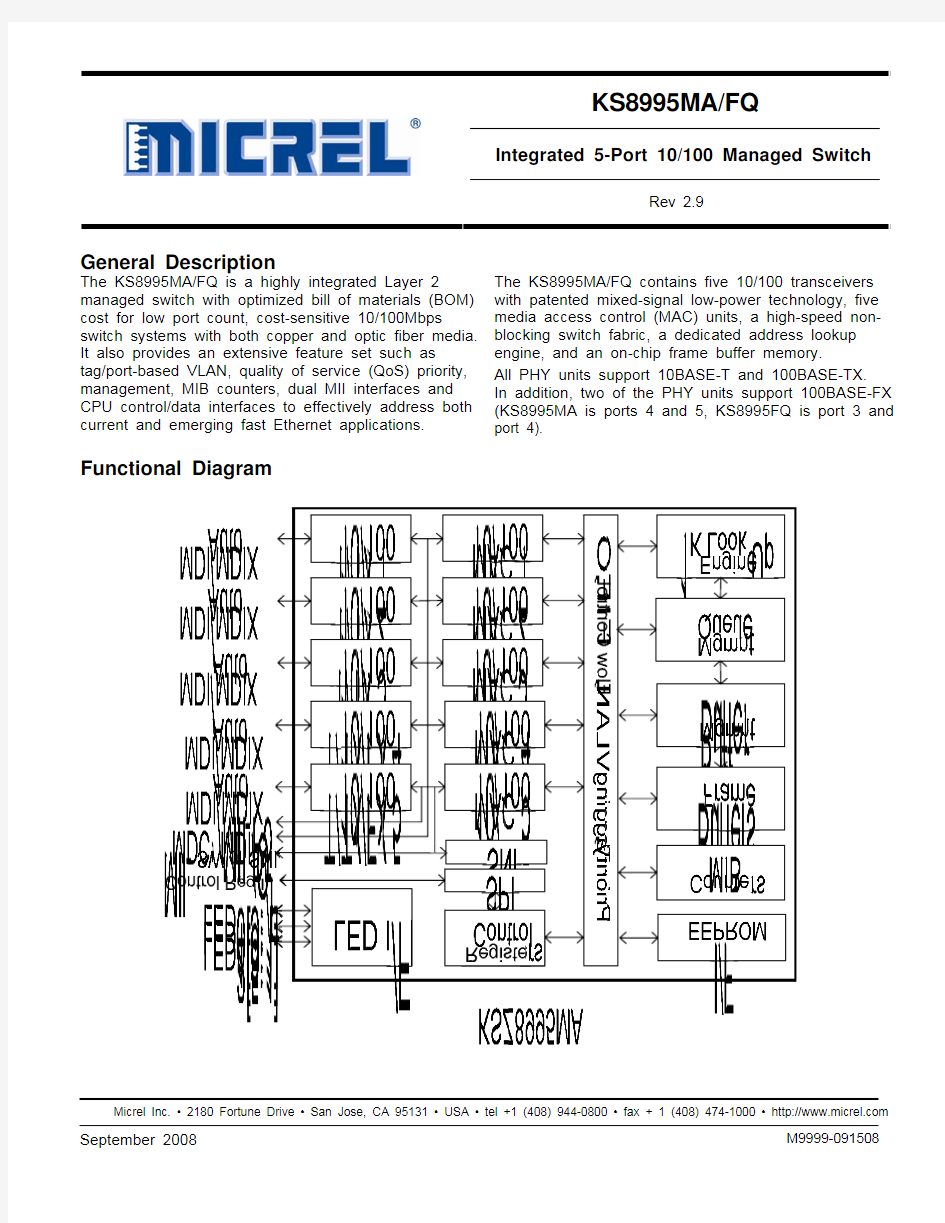
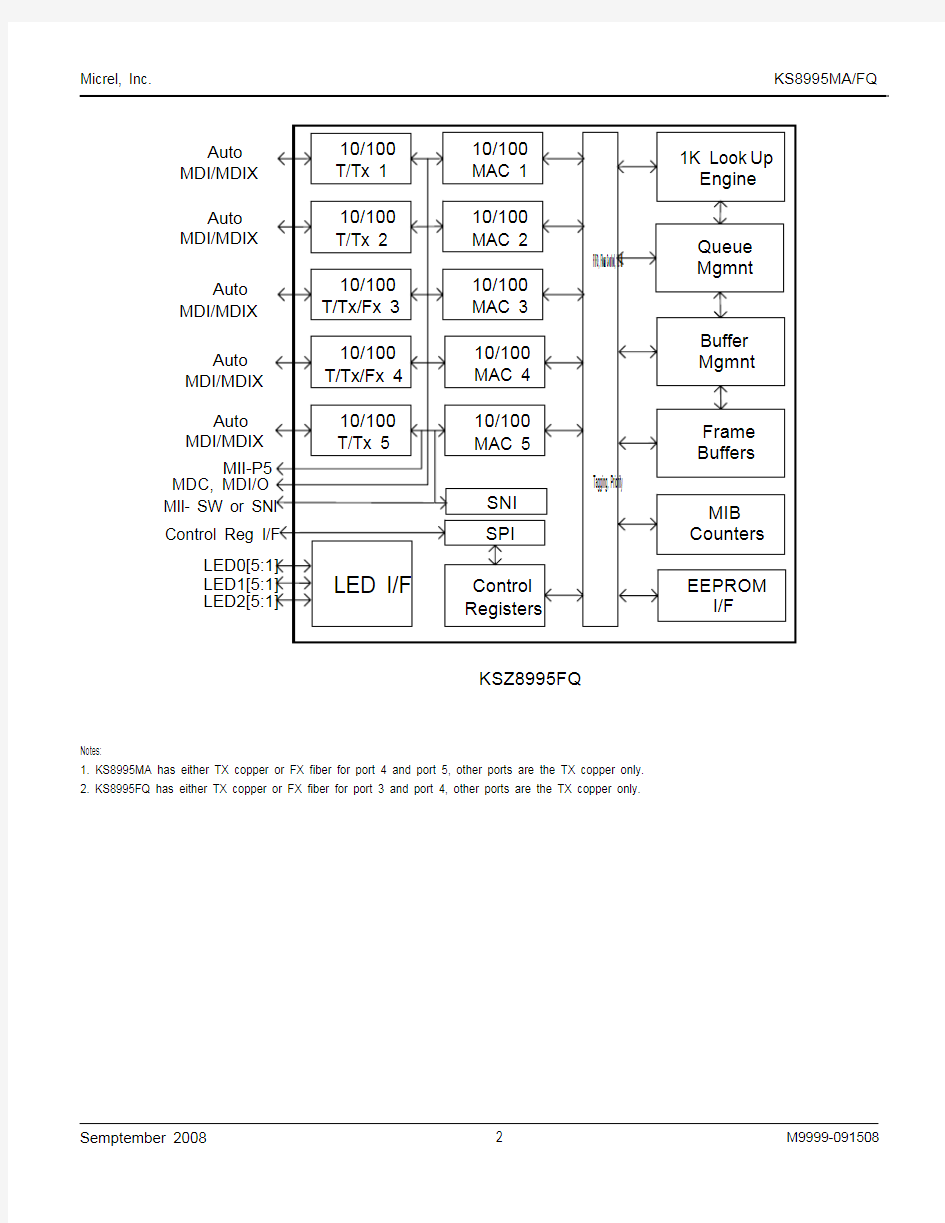
The KS8995MA/FQ is a highly integrated Layer 2
managed switch with optimized bill of materials (BOM)
cost for low port count, cost-sensitive 10/100Mbps
switch systems with both copper and optic fiber media.
It also provides an extensive feature set such as
tag/port-based VLAN, quality of service (QoS) priority,
management, MIB counters, dual MII interfaces and
CPU control/data interfaces to effectively address both
current and emerging fast Ethernet applications.
The KS8995MA/FQ contains five 10/100 transceivers
with patented mixed-signal low-power technology, five
media access control (MAC) units, a high-speed non-
blocking switch fabric, a dedicated address lookup
engine, and an on-chip frame buffer memory.
All PHY units support 10BASE-T and 100BASE-TX.
In addition, two of the PHY units support 100BASE-FX
(KS8995MA is ports 4 and 5, KS8995FQ is port 3 and
port 4).
Functional Diagram
Auto MDI/MDIX MII-MDC, MDI/O Auto MDI/MDIX Auto MDI/MDIX Auto MDI/MDIX Auto MDI/MDIX KSZ8995FQ
Notes:
1. KS8995MA has either TX copper or FX fiber for port 4 and port 5, other ports are the TX copper only.
2. KS8995FQ has either TX copper or FX fiber for port 3 and port 4, other ports are the TX copper only.
Features
?Integrated switch with five MACs and five fast Ethernet transceivers fully compliant to IEEE 802.3u standard
?Shared memory based switch fabric with fully non-blocking configuration
? 1.4Gbps high-performance memory bandwidth
?10BASE-T, 100BASE-TX, and 100BASE-FX modes ?Dual MII configuration: MII-Switch (MAC or PHY mode MII) and MII-P5 (PHY mode MII)
?IEEE 802.1q tag-based VLAN (16 VLANs, full-range VID) for DMZ port, WAN/LAN separation or inter-
VLAN switch links
?VLAN ID tag/untag options, per-port basis ?Programmable rate limiting 0Mbps to 100Mbps, ingress and egress port, rate options for high and low priority, per-port basis in 32Kbps increments
?Flow control or drop packet rate limiting (ingress port) ?Integrated MIB counters for fully compliant statistics gathering, 34 MIB counters per port
?Enable/Disable option for huge frame size up to 1916 bytes per frame
?IGMP v1/v2 snooping for multicast packet filtering ?Special tagging mode to send CPU info on ingress packet’s port value
?SPI slave (complete) and MDIO (MII PHY only) serial management interface for control of register
configuration
?MAC-id based security lock option
?Control registers configurable on-the-fly (port-priority, 802.1p/d/q, AN...)
?CPU read access to MAC forwarding table entries ?802.1d Spanning Tree Protocol
?Port mirroring/monitoring/sniffing: ingress and/or egress traffic to any port or MII
?Broadcast storm protection with % control – global and per-port basis
?Optimization for fiber-to-copper media conversion ?Full-chip hardware power-down support (register configuration not saved) ?Per-port based software power-save on PHY (idle link detection, register configuration preserved) ?QoS/CoS packets prioritization supports: per port, 802.1p and DiffServ based
?802.1p/q tag insertion or removal on a per-port basis (egress)
?MDC and MDI/O interface support to access the MII PHY control registers (not all control registers) ?MII local loopback support
?On-chip 64Kbyte memory for frame buffering (not shared with 1K unicast address table)
?Wire-speed reception and transmission ?Integrated look-up engine with dedicated 1K MAC addresses
?Full duplex IEEE 802.3x and half-duplex back pressure flow control
?Comprehensive LED support
?7-wire SNI support for legacy MAC interface ?Automatic MDI/MDI-X crossover for plug-and-play ?Disable automatic MDI/MDI-X option
? Low power:
Core: 1.8V
Digital I/O: 3.3V
Analog I/O: 2.5V or 3.3V
?0.18μm CMOS technology
?Commercial temperature range: 0°C to +70°C ?Industrial temperature range: –40°C to +85°C ?Available in 128-pin PQFP package
Applications
? Broadband gateway/firewall/VPN
?Integrated DSL or cable modem multi-port router ?Wireless LAN access point plus gateway
?Home networking expansion
?Standalone 10/100 switch
? Hotel/campus/MxU gateway
?Enterprise VoIP gateway/phone
?FTTx customer premise equipment
?Managed Media converter
Ordering Information
Part Number
Standard Pb-Free Temperature
Range
Package
KS8995MA KSZ8995MA 0°C to +70°C 128-Pin PQFP KS8995FQ KSZ8995FQ 0°C to +70°C 128-Pin PQFP KS8995MAI KSZ8995MAI –40°C to +85°C 128-Pin PQFP KS8995FQI KSZ8995FQI –40°C to +85°C 128-Pin PQFP
Revision History
Revision Date Summary of Changes
2.0 10/10/03 Created.
2.1 10/30/03 Editorial changes on electrical characteristics.
2.2 4/01/04 Editorial changes on the TTL input and output electrical characteristics. 2.3
1/19/05
Insert recommended reset circuit, pg. 70. Editorial, Pg. 36.
2.4 4/13/05
Changed VDDIO to 3.3V. Changed Jitter to 16 ns Max. 2.5
2/6/06
Added Pb-Free option for Industrial version.
2.6 7/12/06 Add a note for VLAN table write, improve the timing diagram for MII interface, update pin
description for PCRS, PCOL, etc. And update the description of the register bits for the
loopback, etc. 2.7 6/01/07
Add the package thermal information in the operating rating and the transformer power
consumption information in the electrical characteristics note. 2.8 03/20/08 Add KSZ8995FQ information and pin description.
2.9
09/15/08
Add KSZ8995FQ block diagram and descriptions for revision ID and LED mode.
Contents
System Level Applications (8)
Pin Configuration (10)
Pin Description (by Number) (11)
Pin Description (by Name) (17)
Introduction (23)
Functional Overview: Physical Layer Transceiver (23)
100BASE-TX Transmit (23)
100BASE-TX Receive (23)
PLL Clock Synthesizer (23)
Scrambler/De-Scrambler (100BASE-TX only) (24)
100BASE-FX Operation (24)
100BASE-FX Signal Detection (24)
100BASE-FX far End fault (24)
10BASE-T Transmit (24)
10BASE-T Receive (24)
Power Management (24)
MDI/MDI-X Auto Crossover (24)
Auto-Negotiation (24)
Functional Overview: Switch Core (25)
Address Look-Up (25)
Learning (25)
Migration (25)
Aging (25)
Forwarding (25)
Switching Engine (26)
Media Access Controller (MAC) Operation (26)
Inter-Packet Gap (IPG) (26)
Backoff Algorithm (26)
Late Collision (26)
Illegal Frames (26)
Flow Control (26)
Half-Duplex Back Pressure (28)
Broadcast Storm Protection (28)
MII Interface Operation (29)
SNI Interface Operation (31)
Advanced Functionality (31)
Spanning Tree Support (31)
Special Tagging Mode (32)
IGMP Support (33)
Port Mirroring Support (34)
VLAN Support (34)
Rate Limit Support (35)
Configuration Interface (36)
I2C Master Serial Bus Configuration (38)
SPI Slave Serial Bus Configuration (38)
MII Management Interface (MIIM) (41)
Register Description (42)
Global Registers (43)
Register 0 (0x00): Chip ID0 (43)
Register 1 (0x01): Chip ID1 / Start Switch (43)
Register 2 (0x02): Global Control 0 (43)
Register 3 (0x03): Global Control 1 (43)
Register 4 (0x04): Global Control 2 (44)
Register 5 (0x05): Global Control 3 (45)
Register 8 (0x08): Global Control 6 (46)
Register 9 (0x09): Global Control 7 (46)
Register 10 (0x0A): Global Control 8 (47)
Register 11 (0x0B): Global Control 9 (47)
Port Registers (48)
Register 16 (0x10): Port 1 Control 0 (48)
Register 17 (0x11): Port 1 Control 1 (49)
Register 18 (0x12): Port 1 Control 2 (49)
Register 19 (0x13): Port 1 Control 3 (50)
Register 20 (0x14): Port 1 Control 4 (50)
Register 21 (0x15): Port 1 Control 5 (51)
Register 22 (0x16): Port 1 Control 6 (51)
Register 23 (0x17): Port 1 Control 7 (51)
Register 24 (0x18): Port 1 Control 8 (51)
Register 25 (0x19): Port 1 Control 9 (52)
Register 26 (0x1A): Port 1 Control 10 (52)
Register 27 (0x1B): Port 1 Control 11 (52)
Register 28 (0x1C): Port 1 Control 12 (53)
Register 29 (0x1D): Port 1 Control 13 (54)
Register 30 (0x1E): Port 1 Status 0 (54)
Register 31 (0x1F): Port 1 Control 14 (55)
Advanced Control Registers (55)
Register 96 (0x60): TOS Priority Control Register 0 (55)
Register 97 (0x61): TOS Priority Control Register 1 (55)
Register 98 (0x62): TOS Priority Control Register 2 (55)
Register 99 (0x63): TOS Priority Control Register 3 (55)
Register 100 (0x64): TOS Priority Control Register 4 (55)
Register 101 (0x65): TOS Priority Control Register 5 (56)
Register 102 (0x66): TOS Priority Control Register 6 (56)
Register 103 (0x67): TOS Priority Control Register 7 (56)
Register 104 (0x68): MAC Address Register 0 (56)
Register 105 (0x69): MAC Address Register 1 (56)
Register 106 (0x6A): MAC Address Register 2 (56)
Register 107 (0x6B): MAC Address Register 3 (56)
Register 108 (0x6C): MAC Address Register 4 (56)
Register 109 (0X6D): MAC Address Register 5 (56)
Register 110 (0x6E): Indirect Access Control 0 (56)
Register 111 (0x6F): Indirect Access Control 1 (56)
Register 112 (0x70): Indirect Data Register 8 (56)
Register 113 (0x71): Indirect Data Register 7 (57)
Register 114 (0x72): Indirect Data Register 6 (57)
Register 115 (0x73): Indirect Data Register 5 (57)
Register 116 (0x74): Indirect Data Register 4 (57)
Register 117 (0x75): Indirect Data Register 3 (57)
Register 118 (0x76): Indirect Data Register 2 (57)
Register 119 (0x77): Indirect Data Register 1 (57)
Register 120 (0x78): Indirect Data Register 0 (57)
Register 121 (0x79): Digital Testing Status 0 (57)
Register 122 (0x7A): Digital Testing Status 1 (57)
Register 123 (0x7B): Digital Testing Control 0 (57)
Register 124 (0x7C): Digital Testing Control 1 (57)
Register 125 (0x7D): Analog Testing Control 0 (57)
Register 126 (0x7E): Analog Testing Control 1 (57)
Register 127 (0x7F): Analog Testing Status (57)
Dynamic MAC Address (61)
MIB Counters (62)
MIIM Registers (65)
Register 0: MII Control (65)
Register 1: MII Status (65)
Register 2: PHYID HIGH (66)
Register 3: PHYID LOW (66)
Register 4: Advertisement Ability (66)
Register 5: Link Partner Ability (66)
Absolute Maximum Ratings(1) (67)
Operating Ratings(2) (67)
Electrical Characteristics(4, 5) (67)
Timing Diagrams (69)
Selection of Isolation Transformer(1) (77)
Package Information (78)
System Level Applications
4-port LAN
1-port WAN I/F
Figure 1. Broadband Gateway
4-port LAN
Figure 2. Integrated Broadband Router
5-port LAN
Figure 3. Standalone Switch
Figure 4. Using KSZ8995FQ for Dual Media Converter or Fiber daisy chain connection
Pin Configuration
128-Pin PQFP
Pin Description (by Number)
Pin Number
Pin Name
Type (1)
Port
Pin Function (2)
1 MDI-XDIS lpd 1-5 Disable auto MDI/MDI-X.
PD (default) = normal operation.
PU = disable auto MDI/MDI-X on all ports. 2 GNDA Gnd Analog ground. 3 VDDAR P 1.8V analog V DD .
4 RXP1 I 1 Physical receive signal + (differential). 5
RXM1
I
1
Physical receive signal – (differential). 6 GNDA Gnd Analog ground.
7 TXP1 O 1 Physical transmit signal + (differential). 8
TXM1
O
1
Physical transmit signal – (differential). 9 VDDAT P 2.5V or 3.3V analog V DD .
10 RXP2 I 2 Physical receive signal + (differential). 11
RXM2
I
2
Physical receive signal – (differential). 12 GNDA Gnd Analog ground.
13 TXP2 O 2 Physical transmit signal + (differential). 14
TXM2
O
2
Physical transmit signal – (differential). 15 VDDAR P 1.8V analog V DD . 16 GNDA Gnd Analog ground.
17 ISET
Set physical transmit output current. Pull-down with a
3.01k ?1% resistor. 18 VDDAT P 2.5V or 3.3V analog V DD .
19 RXP3 I 3 Physical receive signal + (differential). 20
RXM3
I
3
Physical receive signal - (differential). 21 GNDA Gnd Analog ground.
22 TXP3 O 3 Physical transmit signal + (differential). 23
TXM3
O
3
Physical transmit signal – (differential). 24 VDDAT P 2.5V or 3.3V analog V DD .
25 RXP4 I 4 Physical receive signal + (differential). 26
RXM4
I
4
Physical receive signal - (differential). 27 GNDA Gnd Analog ground.
28 TXP4 O 4 Physical transmit signal + (differential). 29
TXM4
O
4
Physical transmit signal – (differential). 30 GNDA Gnd
Analog ground.
Notes:
1. P = Power supply. I = Input. O = Output. I/O = Bidirectional. Gnd = Ground. Ipu = Input w/internal pull-up. Ipd = Input w/internal pull-down. Ipd/O = Input w/internal pull-down during reset, output pin otherwise. Ipu/O = Input w/internal pull-up during reset, output pin otherwise. NC = No connect.
2. PU = Strap pin pull-up. PD = Strap pull-down.
Pin Number
Pin Name Type (1) Port Pin Function 31 VDDAR P 1.8V analog V DD .
32 RXP5 I 5 Physical receive signal + (differential). 33
RXM5
I
5
Physical receive signal – (differential). 34 GNDA Gnd Analog ground.
35 TXP5 O 5 Physical transmit signal + (differential). 36
TXM5
O
5
Physical transmit signal – (differential). 37 VDDAT P
2.5V or
3.3V analog V DD .
38 FXSD5/FXSD3 Ipd 5/3
Fiber signal detect pin. FXSD5 is for port 5 of the KS8995MA. FXSD3 is for port 3 of the KS8995FQ 39
FXSD4
Ipd
4
Fiber signal detect pin for port 4. 40 GNDA Gnd Analog ground. 41 VDDAR P 1.8V analog V DD . 42 GNDA Gnd Analog ground. 43 VDDAR P 1.8V analog V DD . 44 GNDA Gnd Analog ground.
45 MUX1 NC Factory test pins. MUX1 and MUX2 should be left unconnected for
normal operation
Mode MUX1 MUX2 46 MUX2 NC Normal Operation NC NC 47 PWRDN_N Ipu Full-chip power down. Active low. 48 RESERVE NC
Reserved pin. No connect. 49 GNDD Gnd Digital ground. 50 VDDC P 1.8V digital core V DD . 51 PMTXEN Ipd 5 PHY[5] MII transmit enable. 52 PMTXD3 Ipd 5 PHY[5] MII transmit bit 3. 53 PMTXD2 Ipd 5 PHY[5] MII transmit bit 2. 54 PMTXD1 Ipd 5 PHY[5] MII transmit bit 1. 55 PMTXD0 Ipd 5 PHY[5] MII transmit bit 0. 56 PMTXER Ipd 5 PHY[5] MII transmit error.
57
PMTXC
O
5
PHY[5] MII transmit clock. PHY mode MII. 58 GNDD Gnd Digital ground.
59 VDDIO P 3.3V digital V DD for digital I/O circuitry. 60
PMRXC
O
5
PHY[5] MII receive clock. PHY mode MII.
Notes:
1. P = Power supply. I = Input. O = Output. I/O = Bidirectional. Gnd =
Ground. Ipu = Input w/internal pull-up. Ipd = Input w/internal pull-down. Ipd/O = Input w/internal pull-down during reset, output pin otherwise. Ipu/O = Input w/internal pull-up during reset, output pin otherwise. NC = No connect.
Pin Number
Pin Name Type (1) Port Pin Function (2)
61
PMRXDV
Ipd/O
5
PHY[5] MII receive data valid.
62 PMRXD3 Ipd/O 5
PHY[5] MII receive bit 3. Strap option: PD (default) = enable flow control;
PU = disable flow control. 63 PMRXD2 Ipd/O 5
PHY[5] MII receive bit 2. Strap option: PD (default) = disable back
pressure; PU = enable back pressure. 64 PMRXD1 Ipd/O 5
PHY[5] MII receive bit 1. Strap option: PD (default) = drop excessive
collision packets; PU = does not drop excessive collision packets. 65 PMRXD0 Ipd/O 5
PHY[5] MII receive bit 0. Strap option: PD (default) = disable aggressive back-off algorithm in half-duplex mode; PU = enable for performance enhancement. 66 PMRXER Ipd/O 5
PHY[5] MII receive error. Strap option: PD (default) = packet size
1518/1522 bytes; PU = 1536 bytes. 67 PCRS Ipd/O 5 PHY[5] MII carrier sense/strap option for port 4 only. PD (default) = force
half-duplex if auto-negotiation is disabled or fails. PU = force full-duplex
if auto negotiation is disabled or fails. Refer to Register 76. 68 PCOL Ipd/O 5
PHY[5] MII collision detect/ strap option for port 4 only. PD (default) = no force flow control, normal operation. PU = force flow control. Refer to Register 66 69 SMTXEN Ipd Switch MII transmit enable. 70 SMTXD3 Ipd Switch MII transmit bit 3. 71 SMTXD2 Ipd Switch MII transmit bit 2. 72 SMTXD1 Ipd Switch MII transmit bit 1. 73 SMTXD0 Ipd Switch MII transmit bit 0. 74 SMTXER Ipd Switch MII transmit error.
75 SMTXC I/O Switch MII transmit clock. Input in MAC mode, output in PHY mode MII. 76 GNDD Gnd Digital ground.
77 VDDIO P 3.3V digital V DD for digital I/O circuitry.
78 SMRXC I/O Switch MII receive clock. Input in MAC mode, output in PHY mode MII. 79 SMRXDV Ipd/O Switch MII receive data valid.
80 SMRXD3 Ipd/O Switch MII receive bit 3. Strap option: PD (default) = Disable Switch MII
full-duplex flow control; PU = Enable Switch MII full-duplex flow control. 81 SMRXD2 Ipd/O
Switch MII receive bit 2. Strap option: PD (default) = Switch MII in full-duplex mode; PU = Switch MII in half-duplex mode.
Notes: 1. P = Power supply. I = Input. O = Output. I/O = Bidirectional. Gnd =
Ground. Ipu = Input w/internal pull-up. Ipd = Input w/internal pull-down. Ipd/O = Input w/internal pull-down during reset, output pin otherwise. Ipu/O = Input w/internal pull-up during reset, output pin otherwise. NC = No connect. 2. PU = Strap pin pull-up. PD = Strap pull-down.
Pin Number
Pin Name
Type (1)
Port
Pin Function (2)
82 SMRXD1 Ipd/O
Switch MII receive bit 1. Strap option: PD (default) = Switch MII in 100Mbps mode; PU = Switch MII in 10Mbps mode. Switch MII receive bit 0; Strap option: LED mode
PD (default) = mode 0; PU = mode 1. See “Register 11.” Mode 0, link at
100/Full LEDx[2,1,0]=0,0,0 100/Half LEDx[2,1,0]=0,1,0 10/Full LEDx[2,1,0]=0,0,1 10/Half LEDx[2,1,0]=0,1,1
Mode 1, link at
100/Full LEDx[2,1,0]=0,1,0 100/Half LEDx[2,1,0]=0,1,1 10/Full LEDx[2,1,0]=1,0,0 10/Half LEDx[2,1,0]=1,0,1
Mode 0 Mode 1 LEDX_2 Lnk/Act 100Lnk/Act LEDX_1 Fulld/Col 10Lnk/Act 83 SMRXD0 Ipd/O
LEDX_0 Speed Full duplex
84 SCOL Ipd/O Switch MII collision detect. 85 SCRS Ipd/O Switch mode carrier sense.
86 SCONF1 Ipd
Dual MII configuration pin. For the Switch MII, KSZ8995MA supports both MAC mode and PHY mode, KSZ8995FQ supports PHY mode only.
Pin# (91, 86, 87): Switch MII PHY [5] MII 000 Disable, Otri Disable, Otri 001 PHY Mode MII Disable, Otri 010
MAC Mode MII Disable, Otri 011 PHY Mode SNI Disable, Otri 100 Disable Disable 101 PHY Mode MII PHY Mode MII 110 MAC Mode MII PHY Mode MII
111
PHY Mode SNI
PHY Mode MII
87 SCONF0 Ipd Dual MII configuration pin. 88 GNDD Gnd Digital ground. 89 VDDC P
1.8V digital core V DD .
90 LED5-2 Ipu/O 5
LED indicator 2. Strap option: aging setup. See “Aging” section. PU (default) = aging enable; PD = aging disable.
91 LED5-1 Ipu/O 5
LED indicator 1. Strap option: PU (default): enable PHY[5] MII I/F. PD:
tristate all PHY[5] MII output. See “Pin 86 SCONF1.”
Notes: 1. P = Power supply. I = Input. O = Output. I/O = Bidirectional. Gnd =
Ground. Ipu = Input w/internal pull-up. Ipd = Input w/internal pull-down. Ipd/O = Input w/internal pull-down during reset, output pin otherwise. Ipu/O = Input w/internal pull-up during reset, output pin otherwise. NC = No connect. 2. PU = Strap pin pull-up. PD = Strap pull-down. Otri = Output tristated. Fulld = Full duplex
Pin Number
Pin Name Type (1) Port Pin Function 92 LED5-0 Ipu/O 5 LED indicator 0. 93 LED4-2 Ipu/O 4 LED indicator 2. 94 LED4-1 Ipu/O 4
LED indicator 1.
95 LED4-0 Ipu/O 4 LED indicator 0.
96 LED3-2 Ipu/O 3 LED indicator 2. 97 LED3-1 Ipu/O 3 LED indicator 1. 98
LED3-0
Ipu/O
3
LED indicator 0. 99 GNDD Gnd Digital ground.
100 VDDIO P 3.3V digital V DD for digital I/O. 101 LED2-2 Ipu/O 2 LED indicator 2. 102 LED2-1 Ipu/O 2 LED indicator 1. 103 LED2-0 Ipu/O 2 LED indicator 0. 104 LED1-2 Ipu/O 1 LED indicator 2. 105 LED1-1 Ipu/O 1 LED indicator 1. 106 LED1-0 Ipu/O 1 LED indicator 0.
107
MDC
Ipu
All
Switch or PHY[5] MII management data clock.
108 MDIO I/O All
Switch or PHY[5] MII management data I/O.
Features internal pull down to define pin state when not driven. 109 SPIQ Otri All
(1) SPI serial data output in SPI slave mode; (2) output clock at 61kHz
in I 2C master mode. See “Pin 113.” 110 SPIC/SCL I/O All (1) Input clock up to 5MHz in SPI slave mode; (2) output clock at 61kHz
in I 2
C master mode. See “Pin 113.” 111 SSPID/SDA I/O All
(1) Serial data input in SPI slave mode; (2) serial data input/output in
I 2C master mode. See “Pin 113.” 112 SPIS_N Ipu All
Active low. (1) SPI data transfer start in SPI slave mode. When SPIS_N is high, the KS8995MA/FQ is deselected and SPIQ is held in high
impedance state, a high-to-low transition to initiate the SPI data transfer; (2) not used in I 2C master mode.
Serial bus configuration pin.
For this case, if the EEPROM is not present, the KS8995MA/FQ will start itself with the PS[1.0] = 00 default register values. Pin Configuration
Serial Bus Configuration
PS[1.0]=00 I 2C Master Mode for EEPROM PS[1.0]=01 Reserved PS[1.0]=10 SPI Slave Mode for CPU Interface 113 PS1 Ipd
PS[1.0]=11
Factory Test Mode (BIST)
Notes:
1. P = Power supply. I = Input. O = Output. I/O = Bidirectional. Gnd = Ground. Ipu = Input w/internal pull-up. Ipd = Input w/internal pull-down. Ipd/O = Input w/internal pull-down during reset, output pin otherwise. Ipu/O = Input w/internal pull-up during reset, output pin otherwise. NC = No connect.
Pin Number
Pin Name
Type (1)
Port
Pin Function
114 PS0 Ipd Serial bus configuration pin. See “Pin 113.” 115 RST_N Ipu Reset the KS8995MA/FQ. Active low. 116 GNDD Gnd Digital ground. 117 VDDC P 1.8V digital core V DD .
118 TESTEN Ipd NC for normal operation. Factory test pin. 119 SCANEN Ipd NC for normal operation. Factory test pin. 120 NC NC No connect.
121 X1 I 25MHz crystal clock connection/or 3.3V tolerant oscillator input. Oscillator should be ±100ppm. 122 X2 O 25MHz crystal clock connection. 123 VDDAP P 1.8V analog V DD for PLL. 124 GNDA Gnd Analog ground. 125 VDDAR P 1.8V analog V DD . 126 GNDA Gnd Analog ground. 127 GNDA Gnd Analog ground.
128 TEST2 NC
NC for normal operation. Factory test pin.
Notes:
1. P = Power supply. I = Input. O = Output. I/O = Bidirectional. Gnd =
Ground. Ipu = Input w/internal pull-up. Ipd = Input w/internal pull-down. Ipd/O = Input w/internal pull-down during reset, output pin otherwise. Ipu/O = Input w/internal pull-up during reset, output pin otherwise. NC = No connect.
Pin Description (by Name)
Pin Number
Pin Name Type (1) Port Pin Function
39 FXSD4 I 4 Fiber signal detect/Factory test pin.
38 FXSD3/FXSD5
I 3/5 Fiber signal detect/Factory test pin for FQ or MA 124 GNDA Gnd Analog ground. 42 GNDA Gnd Analog ground. 44 GNDA Gnd Analog ground. 2 GNDA Gnd Analog ground. 16 GNDA Gnd Analog ground. 30 GNDA Gnd Analog ground. 6 GNDA Gnd Analog ground. 12 GNDA Gnd Analog ground. 21 GNDA Gnd Analog ground. 27 GNDA Gnd Analog ground. 34 GNDA Gnd Analog ground. 40 GNDA Gnd Analog ground. 120 NC NC No connect. 127 GNDA Gnd Analog ground. 126 GNDA Gnd Analog ground. 49 GNDD Gnd Digital ground. 88 GNDD Gnd Digital ground. 116 GNDD Gnd Digital ground. 58 GNDD Gnd Digital ground. 76 GNDD Gnd Digital ground. 99
GNDD
Gnd
Digital ground.
17 ISET
Set physical transmit output current. Pull-down with a 3.01k ?1%
resistor. 106 LED1-0 Ipu/O 1 LED indicator 0. 105 LED1-1 Ipu/O 1 LED indicator 1. 104 LED1-2 Ipu/O 1 LED indicator 2. 103 LED2-0 Ipu/O 2 LED indicator 0. 102 LED2-1 Ipu/O 2 LED indicator 1. 101 LED2-2 Ipu/O 2 LED indicator 2. 98
LED3-0
Ipu/O
3
LED indicator 0.
Notes: 1. P = Power supply. I = Input. O = Output. I/O = Bidirectional. Gnd = Ground. Ipu = Input w/internal pull-up. Ipd = Input w/internal pull-down. Ipd/O = Input w/internal pull-down during reset, output pin otherwise. Ipu/O = Input w/internal pull-up during reset, output pin otherwise. NC = No connect.
Pin Number
Pin Name Type (1) Port Pin Function (2) 97 LED3-1 Ipu/O 3 LED indicator 1. 96 LED3-2 Ipu/O 3 LED indicator 2. 95 LED4-0 Ipu/O 4 LED indicator 0. 94 LED4-1 Ipu/O 4 LED indicator 1. 93 LED4-2 Ipu/O 4 LED indicator 2. 92
LED5-0
Ipu/O
5
LED indicator 0.
91 LED5-1 Ipu/O 5
LED indicator 1. Strap option: PU (default) = enable PHY MII I/F PD: tristate all PHY MII output. See “Pin 86 SCONF1.”
90 LED5-2 Ipu/O 5
LED indicator 2. Strap option: aging setup. See “Aging” section.
(default) = aging enable; PD = aging disable. 107 MDC Ipu All Switch or PHY[5] MII management data clock. 108 MDIO I/O All Switch or PHY[5] MII management data I/O. 1
MDI-XDIS
Ipd
1-5
Disable auto MDI/MDI-X.
45 MUX1 NC
Factory test pins. MUX1 and MUX2 should be left unconnected for
normal operation. 46 MUX2 NC Mode
MUX1 MUX2
Normal Operation
NC
NC
68 PCOL Ipd/O 5
PHY[5] MII collision detect/force flow control. See “Register 18.” For port 4 only. PD (default) = no force flow control. PU = force flow control. 67 PCRS Ipd/O 5
PHY[5] MII carrier sense/force duplex mode. See “Register 28.” For port 4 only. PD (default) = force half-duplex if auto-negotiation is
disabled or fails. PU = force full-duplex if auto-negotiation is disabled or fails. 60
PMRXC
O
5
PHY[5] MII receive clock. PHY mode MII.
65 PMRXD0 Ipd/O 5 PHY[5] MII receive bit 0. Strap option: PD (default) = disable
aggressive back-off algorithm in half-duplex mode; PU = enable for
performance enhancement.
64 PMRXD1 Ipd/O 5
PHY[5] MII receive bit 1. Strap option: PD (default) = drop excessive
collision packets; PU = does not drop excessive collision packets. 63 PMRXD2 Ipd/O 5
PHY[5] MII receive bit 2. Strap option: PD (default) = disable back
pressure; PU = enable back pressure.
62 PMRXD3 Ipd/O 5
PHY[5] MII receive bit 3. Strap option: PD (default) = enable flow
control; PU = disable flow control. 61
PMRXDV
Ipd/O
5
PHY[5] MII receive data valid.
66 PMRXER Ipd/O 5
PHY[5] MII receive error. Strap option: PD (default) = 1522/1518 bytes;
PU = packet size up to 1536 bytes.
Notes: 1. P = Power supply. I = Input. O = Output. I/O = Bidirectional. Gnd = Ground. Ipu = Input w/internal pull-up. Ipd = Input w/internal pull-down. Ipd/O = Input w/internal pull-down during reset, output pin otherwise. Ipu/O = Input w/internal pull-up during reset, output pin otherwise. NC = No connect. 2. PU = Strap pin pull-up. PD = Strap pull-down.
Pin Number
Pin Name Type (1) Port Pin Function
57
PMTXC O 5 PHY[5] MII transmit clock. PHY mode MII. 55 PMTXD0 Ipd 5 PHY[5] MII transmit bit 0. 54 PMTXD1 Ipd 5 PHY[5] MII transmit bit 1. 53 PMTXD2 Ipd 5 PHY[5] MII transmit bit 2. 52 PMTXD3 Ipd 5 PHY[5] MII transmit bit 3. 51 PMTXEN Ipd 5 PHY[5] MII transmit enable. 56
PMTXER Ipd 5 PHY[5] MII transmit error.
114
PS0
Ipd
Serial bus configuration pin. See “Pin 113.”
113 PS1 Ipd
Serial bus configuration pin. If EEPROM is not present, the
KS8995MA/FQ will start itself with chip default (00)...
Pin Configuration
Serial Bus Configuration
PS[1:0]=00 I 2C Master Mode for EEPROM PS[1:0]=01 Reserved
PS[1:0]=10 SPI Slave Mode for CPU Interface PS[1:0]=11
Factory Test Mode (BIST)
47 PWRDN_N Ipu Full-chip power down. Active low.
48 RESERVE NC
Reserved pin. No connect.
115 RST_N Ipu Reset the KS8995MA/FQ. Active low.
5 RXM1 I 1 Physical receive signal – (differential). 11 RXM2 I 2 Physical receive signal – (differential). 20 RXM3 I 3 Physical receive signal – (differential). 2
6 RXM4 I 4 Physical receive signal – (differential). 33 RXM5 I 5 Physical receive signal – (differential). 4 RXP1 I 1 Physical receive signal + (differential). 10 RXP2 I 2 Physical receive signal + (differential). 19 RXP3 I 3 Physical receive signal + (differential). 25 RXP4 I 4 Physical receive signal + (differential). 32 RXP5 I 5 Physical receive signal + (differential). 119 SCANEN Ipd NC for normal operation. Factory test pin. 84 SCOL Ipd/O Switch MII collision detect. 87
SCONF0
Ipd
Dual MII configuration pin.
Notes:
1. P = Power supply. I = Input. O = Output. I/O = Bidirectional. Gnd =
Ground. Ipu = Input w/internal pull-up. Ipd = Input w/internal pull-down. Ipd/O = Input w/internal pull-down during reset, output pin otherwise. Ipu/O = Input w/internal pull-up during reset, output pin otherwise. NC = No connect.
Pin Number
Pin Name
Type (1)
Port
Pin Function (2)
86 SCONF1 Ipd
Dual MII configuration pin. For the Switch MII, KSZ8995MA supports both MAC mode and PHY mode, KSZ8995FQ supports PHY mode only.
Pin# (91, 86, 87): Switch MII PHY [5] MII 000 Disable, Otri Disable, Otri 001 PHY Mode MII Disable, Otri 010
MAC Mode MII Disable, Otri 011 PHY Mode SNI Disable, Otri 100 Disable Disable 101 PHY Mode MII PHY Mode MII 110 MAC Mode MII PHY Mode MII 111
PHY Mode SNI
PHY Mode MII
85 SCRS Ipd/O Switch mode carrier sense.
78 SMRXC I/O
Switch MII receive clock. Input in MAC mode, output in PHY mode MII.
Switch MII receive bit 0; Strap option: LED mode
PD (default) = mode 0; PU = mode 1. See “Register 11.”
Mode 0 Mode 1 LEDX_2 Lnk/Act 100Lnk/Act LEDX_1 Fulld/Col 10Lnk/Act 83 SMRXD0 Ipd/O
LEDX_0 Speed Full duplex 82 SMRXD1 Ipd/O Switch MII receive bit 1. Strap option: PD (default) = Switch MII in 100Mbps mode; PU = Switch MII in 10Mbps mode.
81 SMRXD2 Ipd/O Switch MII receive bit 2. Strap option: PD (default) = Switch MII in full-duplex mode; PU = Switch MII in half-duplex mode.
80 SMRXD3 Ipd/O Switch MII receive bit 3. Strap option: PD (default) = Disable Switch MII full-duplex flow control; PU = Enable Switch MII full-duplex flow control. 79 SMRXDV Ipd/O Switch MII receive data valid.
75 SMTXC I/O Switch MII transmit clock. Input in MAC mode, output in PHY mode MII. 73 SMTXD0 Ipd Switch MII transmit bit 0. 72 SMTXD1 Ipd Switch MII transmit bit 1. 71 SMTXD2 Ipd Switch MII transmit bit 2. 70 SMTXD3 Ipd Switch MII transmit bit 3. 69 SMTXEN Ipd Switch MII transmit enable. 74 SMTXER Ipd
Switch MII transmit error.
Notes: 1. P = Power supply. I = Input. O = Output. I/O = Bidirectional. Gnd =
Ground. Ipu = Input w/internal pull-up. Ipd = Input w/internal pull-down. Ipd/O = Input w/internal pull-down during reset, output pin otherwise. Ipu/O = Input w/internal pull-up during reset, output pin otherwise. Otri = Output tristated. NC = No connect. 2. PU = Strap pin pull-up. PD = Strap pull-down. Fulld = Full duplex