General Description
The MAX5079 ORing MOSFET controller replaces ORing diodes in high-reliability redundant, parallel-con-nected power supplies. Despite their low forward-volt-age drop, ORing Schottky diodes cause excessive power dissipation at high currents. The MAX5079allows for the use of low-on-resistance n-channel power MOSFETs to replace the Schottky diodes. This results in low power dissipation, smaller size, and elimination of heatsinks in high-power applications.
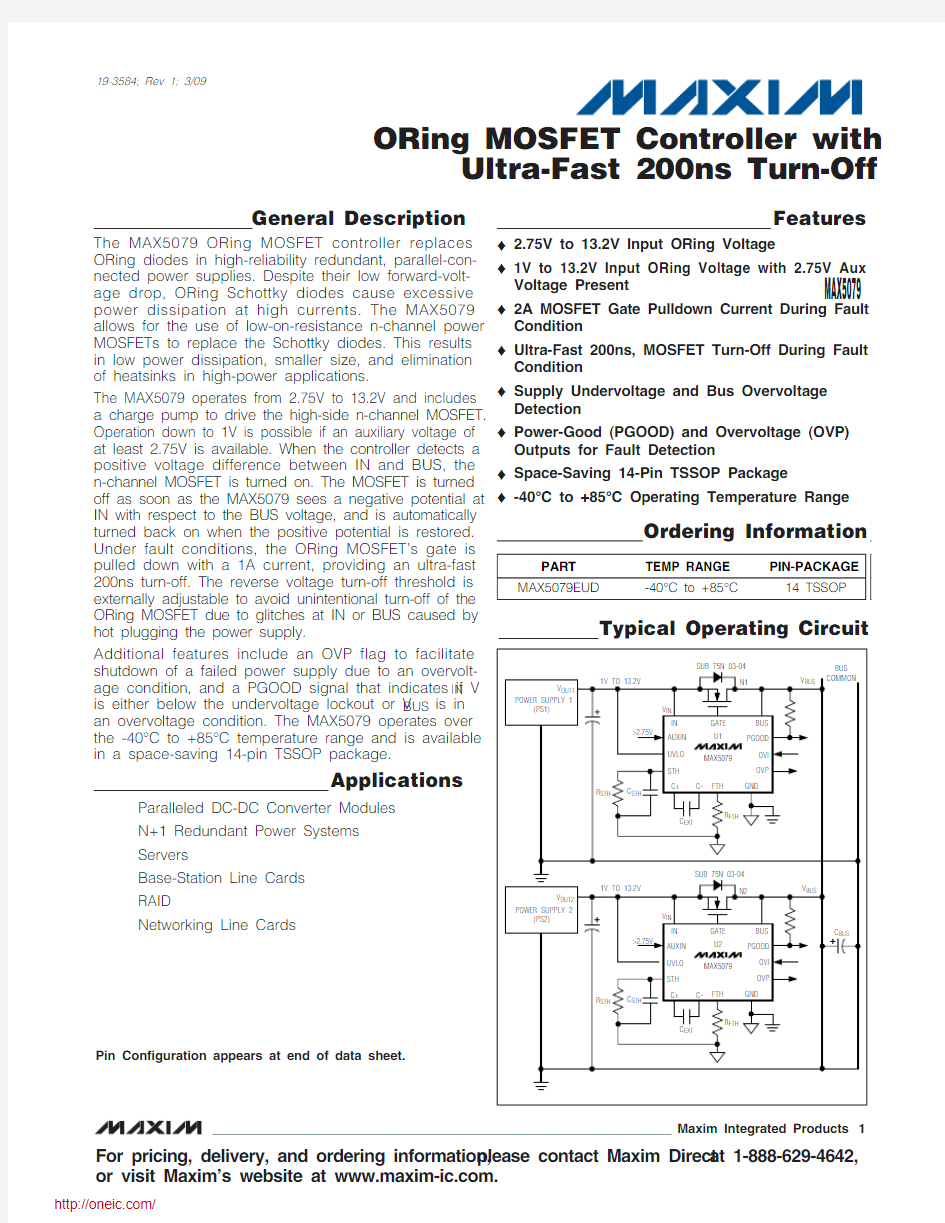
The MAX5079 operates from 2.75V to 13.2V and includes a charge pump to drive the high-side n-channel MOSFET.Operation down to 1V is possible if an auxiliary voltage of at least 2.75V is available. When the controller detects a positive voltage difference between IN and BUS, the n-channel MOSFET is turned on. The MOSFET is turned off as soon as the MAX5079 sees a negative potential at IN with respect to the BUS voltage, and is automatically turned back on when the positive potential is restored.Under fault conditions, the ORing MOSFET’s gate is pulled down with a 1A current, providing an ultra-fast 200ns turn-off. The reverse voltage turn-off threshold is externally adjustable to avoid unintentional turn-off of the ORing MOSFET due to glitches at IN or BUS caused by hot plugging the power supply.
Additional features include an OVP flag to facilitate shutdown of a failed power supply due to an overvolt-age condition, and a PGOOD signal that indicates if V IN is either below the undervoltage lockout or V BUS is in an overvoltage condition. The MAX5079 operates over the -40°C to +85°C temperature range and is available in a space-saving 14-pin TSSOP package.
Applications
Paralleled DC-DC Converter Modules N+1 Redundant Power Systems Servers
Base-Station Line Cards RAID
Networking Line Cards
Features
o 2.75V to 13.2V Input ORing Voltage
o 1V to 13.2V Input ORing Voltage with 2.75V Aux Voltage Present o 2A MOSFET Gate Pulldown Current During Fault Condition o Ultra-Fast 200ns, MOSFET Turn-Off During Fault Condition o Supply Undervoltage and Bus Overvoltage Detection o Power-Good (PGOOD) and Overvoltage (OVP)Outputs for Fault Detection o Space-Saving 14-Pin TSSOP Package o -40°C to +85°C Operating Temperature Range
MAX5079
ORing MOSFET Controller with
Ultra-Fast 200ns Turn-Off
________________________________________________________________Maxim Integrated Products 1
19-3584; Rev 1; 3/09
For pricing, delivery, and ordering information,please contact Maxim Direct at 1-888-629-4642,or visit Maxim’s website at https://www.doczj.com/doc/0613867973.html,.
Typical Operating Circuit
Pin Configuration appears at end of data sheet.
M A X 5079
ORing MOSFET Controller with Ultra-Fast 200ns Turn-Off 2_______________________________________________________________________________________
ABSOLUTE MAXIMUM RATINGS
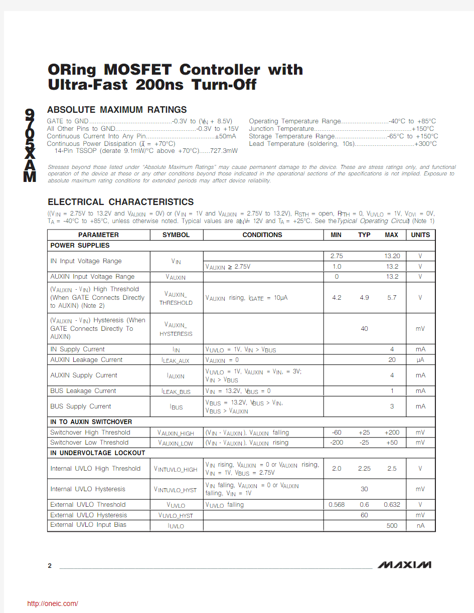
ELECTRICAL CHARACTERISTICS
((V
= 2.75V to 13.2V and V = 0V) or (V = 1V and V = 2.75V to 13.2V), R = open, R = 0, V = 1V, V = 0V, Stresses beyond those listed under “Absolute Maximum Ratings” may cause permanent damage to the device. These are stress ratings only, and functional operation of the device at these or any other conditions beyond those indicated in the operational sections of the specifications is not implied. Exposure to absolute maximum rating conditions for extended periods may affect device reliability.
GATE to GND ..............................................-0.3V to (V IN + 8.5V)All Other Pins to GND.............................................-0.3V to +15V Continuous Current Into Any Pin......................................±50mA Continuous Power Dissipation (T A = +70°C)
14-Pin TSSOP (derate 9.1mW/°C above +70°C)......727.3mW
Operating Temperature Range ...........................-40°C to +85°C Junction Temperature......................................................+150°C Storage Temperature Range.............................-65°C to +150°C Lead Temperature (soldering, 10s).................................+300°C
MAX5079
ORing MOSFET Controller with
Ultra-Fast 200ns Turn-Off
_______________________________________________________________________________________3
ELECTRICAL CHARACTERISTICS (continued)
((V IN = 2.75V to 13.2V and V AUXIN = 0V) or (V IN = 1V and V AUXIN = 2.75V to 13.2V), R STH = open, R FTH = 0, V UVLO = 1V, V OVI = 0V, T A = -40°C to +85°C, unless otherwise noted. Typical values are at V IN = 12V and T A = +25°C. See the Typical Operating Circuit .) (Note 1)
M A X 5079
ORing MOSFET Controller with Ultra-Fast 200ns Turn-Off 4_______________________________________________________________________________________
Note 2: Threshold is reached when charge pump turns off.
Note 3:Gate discharge current is guaranteed through the testing of gate fall time.
Note 4:V IN switchover threshold is V IN at which the gate-drive voltage (V GATE - V IN ) goes from 5V to 7V, V IN rising and (V IN ≥V BUS ).
ELECTRICAL CHARACTERISTICS (continued)
((V IN = 2.75V to 13.2V and V AUXIN = 0V) or (V IN = 1V and V AUXIN = 2.75V to 13.2V), R STH = open, R FTH = 0, V UVLO = 1V, V OVI = 0V, T A = -40°C to +85°C, unless otherwise noted. Typical values are at V IN = 12V and T A = +25°C. See the Typical Operating Circuit .) (Note 1)
Typical Operating Characteristics
(T
A = +25°C, unless otherwise noted. See the Typical Operating Circuit .)
AUXIN SUPPLY CURRENT
vs. TEMPERATURE (V IN = V BUS = 1V)
TEMPERATURE (°C)
I A U X I N (m A )
1109580655035205-10-251
23
-40125
GATE-CHARGE CURRENT vs. V IN
V IN (V)
I G A T E (m A )
14128104620.51.01.52.02.53.03.54.04.55.05.56.00015
131179351SLOW-COMPARATOR REVERSE VOLTAGE
THRESHOLD (V STH vs. R STH )
R STH (k ?)
V S T H (V )
1000.02
0.040.060.08
0.100.120.14
0.160.180.20
010
1000
MAX5079
ORing MOSFET Controller with
Ultra-Fast 200ns Turn-Off
_______________________________________________________________________________________5
020********
50709080100
0.20.30.40.10.50.60.70.90.8 1.0
SLOW-COMPARATOR BLANKING TIME
t STH vs. C STH (R STH = 180k ?)
C STH (μF)
t S T H (m s )
FAST-COMPARATOR REVERSE VOLTAGE
THRESHOLD (V FTH vs. R FTH )
R FTH (k ?)
V F T H (V )
140
120801004060200.10.30.50.20.40.60.70.80.91.01.11.21.31.41.50
0FAST-COMPARATOR RESPONSE TIME
TEMPERATURE (°C)
t R E S P O N S E (n s )
110956580-105203550-258162432404856647280
-40125
CHARGE-PUMP FREQUENCY
vs. INPUT VOLTAGE
V IN (V)
f C P (k H z )
14121011139782345616264666870727476788060
15
GATE-CHARGE CURRENT vs. C EXT
C EXT (nF)
G A T E -C H A R G E C U R R E N T (m A )
100.51.01.52.02.53.54.04.55.06.00
1
100
3.05.5FAULT CURRENT WAVEFORM (IN SHORTED TO PGND)
MAX5079 toc09
V IN = 5V, V BUS = 5V,V AUXIN = 0V, C STH = 0,R STH = OPEN, R FTH = 0,UVLO = IN
BUS 5V/div
IN 5V/div
GATE 10V/div MOSFET REVERSE CURRENT 5A/div 400ns/div
Typical Operating Characteristics (continued)
(T A = +25°C, unless otherwise noted. See the Typical Operating Circuit .)
M A X 5079
ORing MOSFET Controller with Ultra-Fast 200ns Turn-Off 6_______________________________________________________________________________________
Typical Operating Characteristics (continued)
(T A = +25°C, unless otherwise noted. See the Typical Operating Circuit .)
FAULT CURRENT WAVEFORM (IN SHORTED TO PGND)
MAX5079 toc13
V IN = 5V, V BUS = 5V,V AUXIN = 5V, C STH = 0μF,R STH = OPEN, R FTH = 0,UVLO = IN
BUS 5V/div
IN 5V/div
GATE 10V/div MOSFET REVERSE CURRENT 10A/div 1μs/div
FAULT CURRENT WAVEFORM (IN SHORTED TO PGND)MAX5079 toc12V IN = 1V, V BUS = 1V,V AUXIN = 5V, C STH = 0μF,R STH = OPEN, R FTH = 0,UVLO = IN
BUS 1V/div IN 1V/div
GATE 5V/div MOSFET REVERSE CURRENT 10A/div 1μs/div
FAULT CURRENT WAVEFORM (IN SHORTED TO PGND)
MAX5079 toc10
V IN = 2.75V, V BUS = 2.75V,V AUXIN = 0V, C STH = 0μF,R STH = OPEN, R FTH = 0,UVLO = IN
BUS 2V/div
IN 2V/div
GATE 5V/div MOSFET REVERSE CURRENT 10A/div 1μs/div
FAULT CURRENT WAVEFORM (IN SHORTED TO PGND)
MAX5079 toc11
V IN = 12V, V BUS = 12V,V AUXIN = 0V, C STH = 0μF,R STH = OPEN, R FTH = 0,UVLO = IN
BUS 10V/div
IN 10V/div
GATE 20V/div MOSFET REVERSE CURRENT 10A/div 400ns/div
MAX5079
ORing MOSFET Controller with
Ultra-Fast 200ns Turn-Off
_______________________________________________________________________________________7
Typical Operating Characteristics (continued)
(T A = +25°C, unless otherwise noted. See the Typical Operating Circuit .)
FAULT CURRENT WAVEFORM (IN SHORTED TO PGND)
MAX5079 toc14
V IN = 12V, V BUS = 12V,V AUXIN = 5V, C STH = 0,R STH = OPEN, R FTH = 0,UVLO = IN
BUS 10V/div
IN 10V/div
GATE 20V/div MOSFET REVERSE CURRENT 10A/div 1μs/div
POWER-UP WAVEFORM
MAX5079 toc15
V IN = 5.2V, V BUS = 4.9V,I BUS = 5A
BUS 2V/div
CXN 10V/div
GATE 10V/div IN 2V/div 40μs/div
POWER-UP WAVEFORM
MAX5079 toc16
V IN = 12.2V, V BUS = 11.9V,I BUS = 5A
BUS 5V/div
CXN 10V/div
GATE 10V/div IN 5V/div 20μs/div
POWER-UP WAVEFORM
MAX5079 toc17
V IN = 1.2V, V BUS = 1V,V AUXIN = 5V, I BUS = 5A
BUS
500mV/div
CXN 10V/div
GATE 5V/div IN 1V/div 20μs/div
M A X 5079
ORing MOSFET Controller with Ultra-Fast 200ns Turn-Off 8_______________________________________________________________________________________
MAX5079
ORing MOSFET Controller with
Ultra-Fast 200ns Turn-Off
_______________________________________________________________________________________9
Figure 1. Block Diagram
M A X 5079
ORing MOSFET Controller with Ultra-Fast 200ns Turn-Off 10
______________________________________________________________________________________
Detailed Description
The MAX5079 ORing MOSFET controller drives an external n-channel MOSFET and replaces ORing diodes in high-reliability redundant power-management systems or multiple paralleled power supplies. The device has an internal charge pump to drive the high-side n-channel ORing MOSFET. Additional features include an adjustable undervoltage lockout threshold (UVLO), output overvoltage detector (OVI/OVP), input power-good detector (PGOOD), and two programma-ble reverse voltage detectors to detect both fast and slow rises in the reverse voltage across the ORing MOSFET. The input power-supply range is from 2.75V to 13.2V or down to 1V when an auxiliary supply of at least 2.75V is available.
Operational Description
This section describes a detailed startup sequence and behavior of the MAX5079 under different conditions of V BUS and V IN . The MAX5079 powers up whenever V IN is equal to or greater than 2.75V and V UVLO exceeds the UVLO threshold of 0.66V. Operation with V IN down to 1V is possible as long as V UVLO ≥0.6V and V AUXIN ≥2.75V.
When V UVLO crosses the UVLO threshold, V GATE rises to V IN and the charge pump turns on. The charge pump delivers 2mA to charge the gate capacitance of the external MOSFET connected to GATE. The constant gate-charge current prevents large inrush currents from the input supply. During turn-on, the MAX5079 will ignore the reverse voltage at IN with respect to BUS.This is necessary to avoid the unintentional turn-off of the ORing MOSFET as the momentary inrush current causes V IN to dip.
Figure 2 shows the MAX5079 in an ORing configuration with three parallel power supplies (PS1, PS2, and PS3)and three MAX5079s (U1, U2, and U3) provided by out-puts V OUT1, V OUT2, and V OUT3. The following events must be carefully considered to ensure proper function-ality of the MAX5079 ICs.
1)V BUS is zero with a discharged capacitor (C BUS ).All three power supplies are turned ON simulta-neously. V OUT1comes up before V OUT2and V OUT3.
a.When V OUT1turns on, the bus capacitors (C BUS )begin charging from V OUT1through N1’s body diode. When V UVLO (U1) rises above the UVLO threshold, the MAX5079 (U1) charge pump turns on, and U1 monitors the positive potential from V OUT1to V BUS . When V OUT1≥V BUS the charge pump brings GATE (U1) to 5.5V above V IN (U1) (or 7.5V above V IN depending on the magnitude of
V IN ), by sourcing 2mA into N1’s gate capacitance.This results in a less than 10μs turn-on time for the FDB7045L used in the MAX5079 evaluation kit. The fast turn-on is needed to assure that N1 is ON before the rising V OUT1reaches its steady-state value. If the MOSFET is not turned on before V OUT1reaches its steady state, V BUS may overshoot due to the shorting of the 0.7V (forward drop) of N1’s body diode. A higher V IN (U1) can more quickly charge the charge-pump capacitor to 5V (or 7V),while a lower V IN (U1) will take longer. Typically the MOSFET turns on at V GS = 2.5V. Ensure that the soft-start time of the power supply is large enough (> 5ms) to avoid V OUT1racing ahead and causing V BUS to overshoot. Care must be taken to avoid the overloading of V OUT1by either limiting the source current (using the current-sharing circuit) or delay the loading of the BUS until all three power supplies are up and running.
b.V OUT2turns on and begins increasing the voltage at IN (U2). V UVLO (U2) crosses the UVLO thresh-old, the MAX5079 (U2) charge pump turns on and U2 monitors the V OUT2to V BUS voltage. When this voltage difference becomes positive, GATE (U2)begins sourcing 2mA into N2’s gate capacitance.During turn-on, the reverse voltage turn-off circuit is momentarily disabled. If V OUT2is lower than V OUT1, the external load-sharing controller circuit of PS2 will try to increase V OUT2to source current from V OUT2. Assume V OUT2’s rise time is slow enough not to cause any overshoot before N2turns on and starts sharing the current.
c.V OUT3turns on and U3 follows the same sequence as U2. Eventually V OUT1, V OUT2, and V OUT3reach to equilibrium and sharing equal currents.
2)PS1 and PS2 are on and sharing the load when PS3 is hot-inserted. PS3 will take the same course as discussed in 1b above.
a.If V OUT3is higher than V BUS , the BUS voltage will increase to the new level determined by V OUT3.The external load-sharing controller circuit of PS1and PS2 will increase V OUT1and V OUT2to force current sharing.
b.If V OUT3is lower than V BUS , the load-sharing cir-cuit of PS3 will increase V OUT3to force the sharing of current. This causes V OUT3to increases above V BUS . When this voltage difference becomes posi-tive, GATE (U3) begins sourcing 2mA into N3’s gate capacitance. Again, the reverse voltage turn-off circuit is disabled momentarily, as discussed before. The load-sharing circuit of PS3’s controller will adjust V OUT3so as to share the load current.
分销商库存信息:
MAXIM
MAX5079EUD+T MAX5079EVKIT