
1/24/11
https://www.doczj.com/doc/0513860024.html,
1
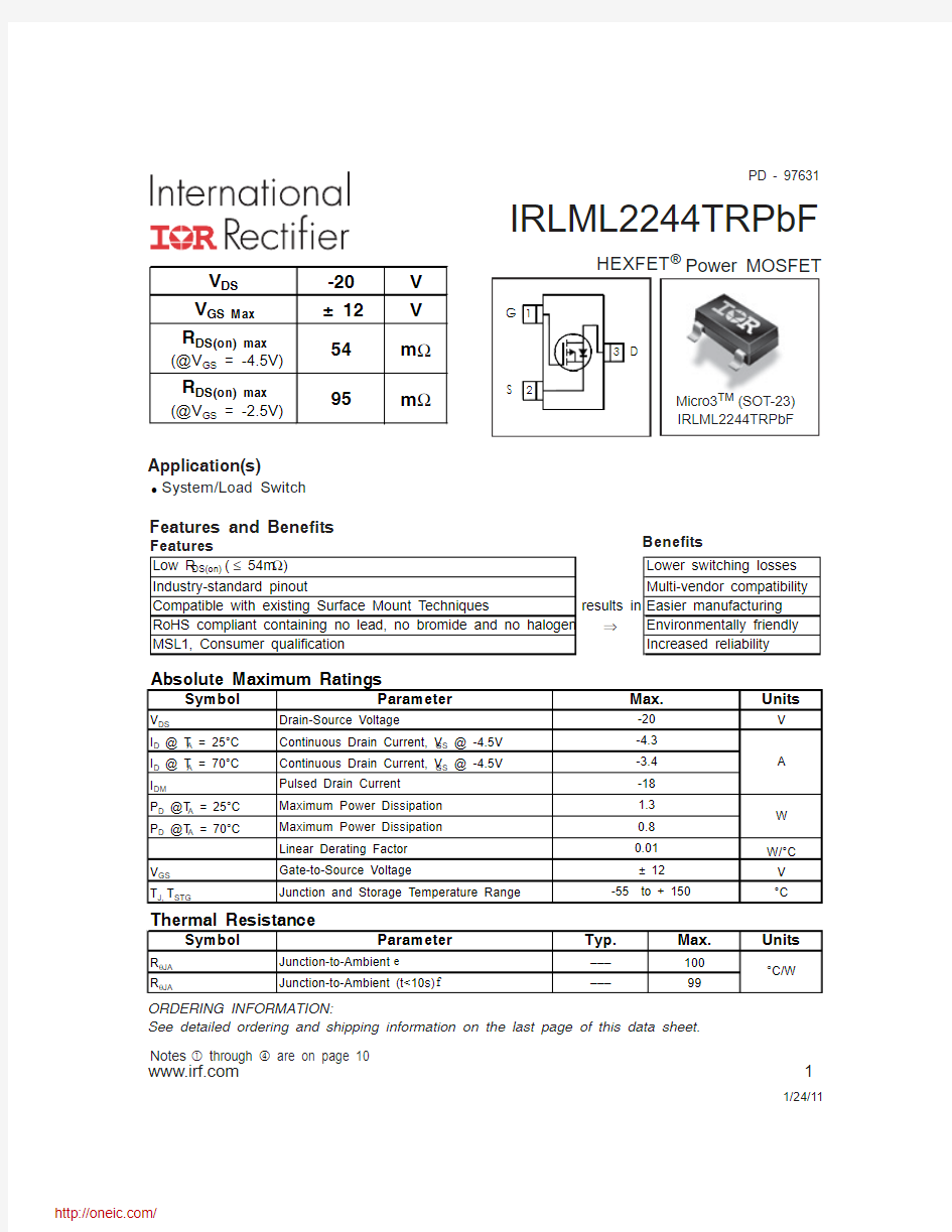
ORDERING INFORMATION:
See detailed ordering and shipping information on the last page of this data sheet.
Notes through are on page 10
Features and Benefits
Benefits
Application(s)
? System/Load Switch
results in ?
IRLML2244TRPbF
https://www.doczj.com/doc/0513860024.html,
IRLML2244TRPbF
https://www.doczj.com/doc/0513860024.html, 3
Fig 2. Typical Output Characteristics
Fig 1. Typical Output Characteristics
Fig 4. Normalized On-Resistance
Vs. Temperature
-V DS , Drain-to-Source Voltage (V)
0.1
1
10
100
-V DS , Drain-to-Source Voltage (V)
-I D , D r a i n -t o -S o u r c e C u r r e n t (A )
T J , Junction Temperature (°C)
R D S (o n ) , D r a i n -t o -S o u r c e O n R e s i s t a n c e
IRLML2244TRPbF
https://www.doczj.com/doc/0513860024.html,
Fig 6. Typical Gate Charge Vs.
Gate-to-Source Voltage
Fig 5. Typical Capacitance Vs.
Drain-to-Source Voltage Fig 8. Maximum Safe Operating Area
Fig 7. Typical Source-Drain Diode
Forward Voltage
1
10
100
-V DS , Drain-to-Source Voltage (V)
10
100
1000
10000
C , C a p a c i t a n c e (p F )
-V SD , Source-to-Drain Voltage (V)
0.1
1
10
100-I S D , R e v e r s e D r a i n C u r r e n t (A )
1
10
100
-V DS , Drain-to-Source Voltage (V)
0.01
0.1
1
10
100
-I D , D r a i n -t o -S o u r c e C u r r e n t (A
)
048121620
Q G
, Total Gate Charge (nC)
2468101214
-V G S , G a t e -t o -S o u r c e V o l t a g e (V )
IRLML2244TRPbF
https://www.doczj.com/doc/0513860024.html, 5
Fig 11. Typical Effective Transient Thermal Impedance, Junction-to-Ambient
Fig 9. Maximum Drain Current Vs.
Ambient Temperature
Fig 10b. Switching Time Waveforms
Fig 10a. Switching Time Test Circuit
25
50
75
100
125
150
T A , Ambient Temperature (°C)
01
2
3
45
-I D , D r a i n C u r r e n t (A
)
t 1 , Rectangular Pulse Duration (sec)
R D
V DD
V DS
V t t t t
https://www.doczj.com/doc/0513860024.html,
Fig 13. Typical On-Resistance Vs. Drain
Current
Fig 12. Typical On-Resistance Vs. Gate
Voltage
Fig 14b. Gate Charge Test Circuit
Fig 14a. Basic Gate Charge Waveform 2
4
6
8
10
12
-V GS, Gate -to -Source Voltage (V)
20
40
60
80
100
120
R D S (o n ), D r a i n -t o -S o u r c e O n R e s i s t a n c e (m Ω
)
5
10
15
20
25
30
35
-I D , Drain Current (A)
040
80
120
160
200
R D S (o n ), D r a i n -t o -S o u r c e O n R e s i s t a n c e (m Ω)
Vgs = -4.5V
Id
Qgs1
Qgs2Qgd Qgodr 0
https://www.doczj.com/doc/0513860024.html, 7
Fig 15. Typical Threshold Voltage Vs.
Junction Temperature
Fig 16. Typical Power Vs. Time
T J , Temperature ( °C )
-V G S (t h ), G a t e t h r e s h o l d V o l t a g e (V )
Time (sec)
P o w e r (W )
IRLML2244TRPbF
https://www.doczj.com/doc/0513860024.html,
Micro3 (SOT-23/TO-236AB) Part Marking Information
Micro3 (SOT-23) Package Outline
Dimensions are shown in millimeters (inches)
Note: For the most current drawing please refer to IR website at: https://www.doczj.com/doc/0513860024.html,/package/
c
F =DA T E C E =X = D =C =B =A =W = (1-26) IF PRECEDED BY LAST DI
G IT O F C ALENDA R YEA R
H =G =K
H G F E D C B 20062003200220052004200820072010
2009J Y 51292830
C B D
52Z
Note: A line a bove the work we e k
(a s s how n he re ) indic a tes Le a d - Fre e.
I =J = IRLML2030L = IRLML0060M = IRLML0040K = IRLML0100N = IRLML2060P = IRLML9301R = IRLML9303
C u HALOG PA
IRLML2244TRPbF
https://www.doczj.com/doc/0513860024.html, 9
Micro3? Tape & Reel Information
Dimensions are shown in millimeters (inches)
2.05 ( .080 )1.95 ( .077 )
TR
FEED DIRECTION
4.1 ( .161 )3.9 ( .154 )
1.6 ( .062 )1.5 ( .060 )
1.85 ( .072 )1.65 ( .065 )
3.55 ( .139 )3.45 ( .136 )
1.1 ( .043 )0.9 ( .036 )4.1 ( .161 )3.9 ( .154 )
0.35 ( .013 )0.25 ( .010 )
8.3 ( .326 )7.9 ( .312 )
1.32 ( .051 )1.12 ( .045 )
9.90 ( .390 )8.40 ( .331 )
178.00( 7.008 ) MAX.
NOTES:
1. CONTROLLING DIMENSION : MILLIMETER.
2. OUTLINE CONFORMS TO EIA-481 & EIA-541.
Note: For the most current drawing please refer to IR website at: https://www.doczj.com/doc/0513860024.html,/package/
IRLML2244TRPbF
https://www.doczj.com/doc/0513860024.html,
Data and specifications subject to change without notice.
IR WORLD HEADQUARTERS: 233 Kansas St., El Segundo, California 90245, USA Tel: (310) 252-7105
TAC Fax: (310) 252-7903
Visit us at https://www.doczj.com/doc/0513860024.html, for sales contact information .01/2011
Qualification standards can be found at International Rectifier’s web site https://www.doczj.com/doc/0513860024.html,/product-info/reliability
Higher qualification ratings may be available should the user have such requirements. Please contact your International Rectifier sales representative for further information: https://www.doczj.com/doc/0513860024.html,/whoto-call/salesrep/
Applicable version of JEDEC standard at the time of product release.
Notes:
Repetitive rating; pulse width limited by max. junction temperature. Pulse width ≤ 400μs; duty cycle ≤ 2%. Surface mounted on 1 in square Cu board Refer to application note #AN-994.
Qualification information ?
分销商库存信息: IR
IRLML2244TRPBF