Surface Mount Bi-Color Chip LEDs MSL-155XX SERIES Description Package Dimensions
The MSL-155xx , a series of bi-color Chip LED device ,
is designed in an industry standard package suitable for
SMT assembly method . This series contain different
combinations of Red & Green chips to provide broad
range choices in wavelength and intensity . They are
all molded in water clear epoxy package.
Features
l Small Size
l Industry Standard Footprint
l Compatible with IR Solder process
l Availalble in 8 mm Tape on 7"(178mm)
Diameter Reels
l Dual color
Applications
l Push-button backlighting
l LCD backlighting
l Symbol backlighting
l Front panel indicator
Absolute Maximum Ratings
@ T A=25o C
Parameter Symbol Units Peak Forward Current I
FP
mA DC Forward Current(1)I F mA
Power Dissipation P
D
mW
Reverse Voltage ( I R = 100 μA )V
R
V
Operating Temperature Range T
OPR
o C
Storage Temperature Range T
STG
o C Notes:
1. Derate linearly as shown in figure 4 for temperatures above 25o C
25
80
Maximum Rating
-30 to + 100
5
-20 to + 80
65
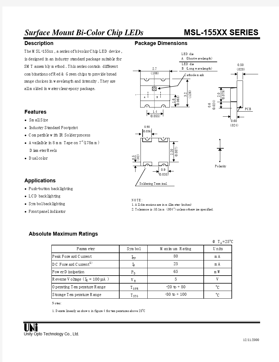
NOTE:
1. All dimensions are in millimeter (inches)
2. Tolerance is ± 0.1mm (.004") unless otherwise specified.
LED die
A (Short wavelength)
0.50
LED die
Polarity
(.024)
Optical-Electrical Characteristics
Luminous
Forward
Viewing Part Intensity Peak Voltage
Angle Number Color
I V (mcd )Wavelength
V F (Volts ) 2 θ 1/2MSL-@ I F = 20 mA
(1)
λpeak
(nm )
@ I F = 20mA Degrees (2)
Min.
Typ.Typ.Typ.Max.Typ.Orange /Yellow Green High eff Red /Yellow Green Super Red /Yellow Green Orange /Pure Green AlGaAs Red /Pure Green Notes:
1.The luminous intensity, IV, is measured at the peak of the spatial radiation pattern which may not be aligned with the mechanical axis of the lamp package.
2. 2θ1/2 is the off-axis angle where the luminous intensity is 1/2 of the peak intensity.
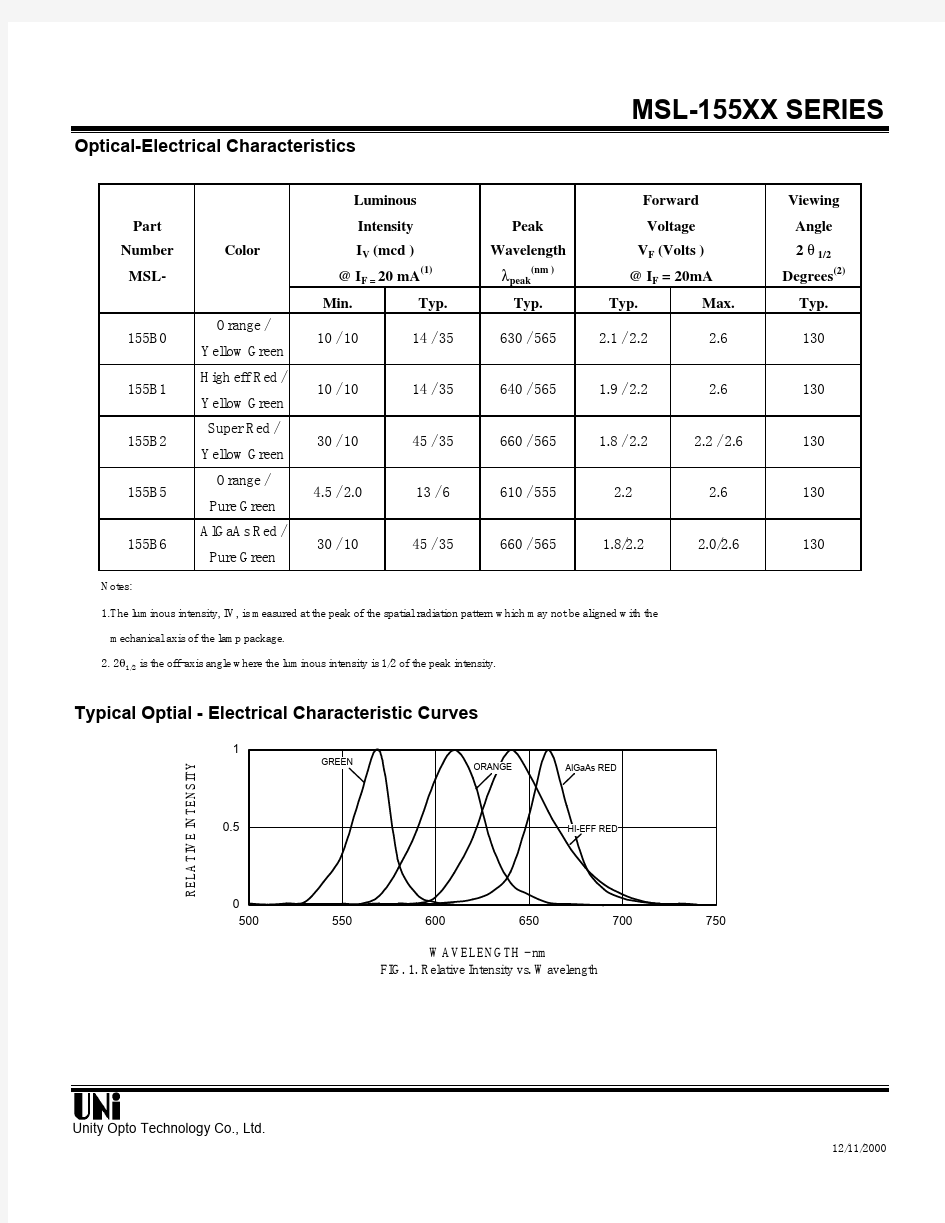
Typical Optial - Electrical Characteristic Curves
1.8/
2.2
2.0/2.6
130
30 / 10
45 / 35
155B6
660 / 565
1301301301302.62.62.2 / 2.62.62.1 / 2.21.9 / 2.21.8 / 2.22.2630 / 565640 / 565660 / 565610 / 55514 / 3514 / 3545 / 3513 / 610 / 1010 / 1030 / 104.5 / 2.0155B0155B1155B2
155B500.5
1
500
550600650700750
WAVELENGTH - nm
FIG. 1. Relative Intensity vs. Wavelength
R E L A T I V E I N T E N S I T Y
Recommended Solder Patterns
Typical Optical - Electrical Characteristic Curves
l DC - DC Forward Current - mA
FIG. 3 RELATIVE LUMINOUS INTENSITY
VS.DC FORWARD CURRENT.
R
e
l
a
t
i
v
e
L
u
m
i
n
o
u
s
I
n
t
e
n
s
i
t
y
(
N
o
r
m
a
l
i
z
e
d
A
t
2
m
A
)
TA - Ambient Temperature - o C
FIG. 4 MAXIMUM DC CURRENT
VS. AMBIENT TEMPERATURE
I
F
-
F
o
r
w
a
r
d
C
u
r
r
e
n
t
-
m
A
20o
30
10o
20o
30
010o
1
.6
.2
N
o
r
m
a
l
i
z
e
d
I
n
t
e
n
s
i
t
y
FIG 5. RADIATION DIAGRAM 0
5
10
15
20
25
30
35
40
020*********
l
F
-
F
o
r
w
a
r
d
C
u
r
r
e
n
t
-
m
A
5
10
15
20
25
30
0.0 1.0 2.0 3.0 4.0
V F - Forward Voltage - V
FIG.2 FORWARD CURRENT
VS. FORWARD VOLTAGE.
0.2
0.4
0.6
0.8
1
1.2
1.4
1.6
0510152025