Features and Benefits
High accuracy relative pressure sensor (+/-1.5%FSO)
Ratiometric Analog Output or digital SENT
output
Fully integrated IC: MEMS, analog front end
circuitry, 16 bit microcontroller, analog back end circuitry, voltage regulators
Large automotive temperature range (-40°C to
150°C)
Automotive qualified and automotive
diagnostic features (clamping levels, broken track diagnostics, multiple internal fault diagnostics)
Factory calibrated and/or fully programmable
through the connector for customized calibration curves
Back side exposed relative pressure sensor
for higher resistance to common automotive media
Assembled in a robust easy to seal package Application Examples
Automotive applications
Vacuum measurement Clogged filter detection Industrial applications
Vacuum sensor Process monitoring
Fluid pressure (low pressure/high
accuracy)
Consumer/Home appliance applications
Filter monitoring
Dispensing/metering systems White goods
Ordering Information
Part No. Temperature Code Package Code Option code MLX90809 L (-40°C to 150°C)
XG EAD-000-RE
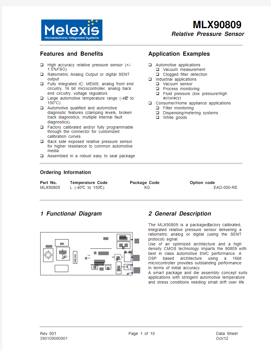
1 Functional Diagram
2 General Description
The MLX90809 is a packaged, factory calibrated, integrated relative pressure sensor delivering a ratiometric analog or digital (using the SENT protocol) signal.
Use of an optimized architecture and a high density CMOS technology imparts the 90809 with best in class automotive EMC performance. A DSP based architecture using a 16bit microcontroller provides outstanding performance in terms of initial accuracy.
A smart package and die assembly concept suits applications with stringent automotive temperature and stress conditions needing small drift over life.
3 Glossary of Terms
Bar: Pressure unit (1bar = 100kPa)
ADC: Analog to Digital Converter
DAC: Digital to Analog Converter
DSP: Digital Signal Processor
EMC: Electro Magnetic Compatibility
SENT: Single Edge Nibble Transmission
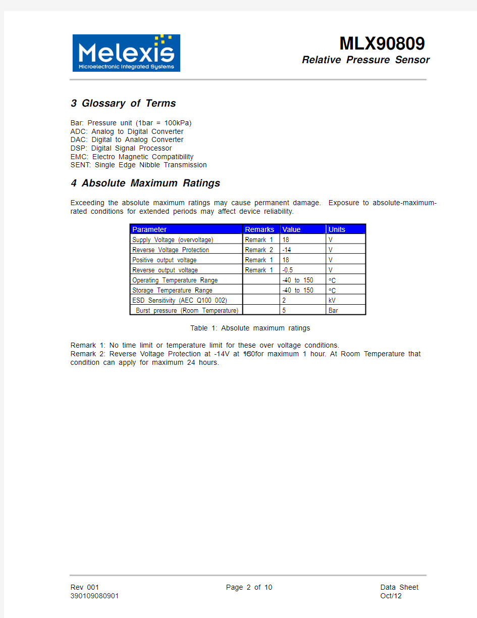
4 Absolute Maximum Ratings
Exceeding the absolute maximum ratings may cause permanent damage. Exposure to absolute-maximum-rated conditions for extended periods may affect device reliability.
Parameter Remarks Value Units
Supply Voltage (overvoltage) Remark 1 18 V
Reverse Voltage Protection Remark 2 -14 V
Positive output voltage Remark 1 18 V
Reverse output voltage Remark 1 -0.5 V
Operating Temperature Range -40 to 150 °C
Storage Temperature Range -40 to 150 °C
ESD Sensitivity (AEC Q100 002) 2 kV
Burst pressure (Room Temperature) 5 Bar
Table 1: Absolute maximum ratings
Remark 1: No time limit or temperature limit for these over voltage conditions.
Remark 2: Reverse Voltage Protection at -14V at 150°C for maximum 1 hour. At Room Temperature that
condition can apply for maximum 24 hours.
5 Pin Definitions and Descriptions
Function / Description YYWW MLXVVVVV-vvv ZZZZZZZZZZ YYWW MLXVVVVV-vvv
ZZZZZZZZZZ
Symbol
VVVVV-vvv
Device used- design revision
YY Year of assembly WW Calendar week of assembly
ZZZZZZZZZZ
Wafer lot number
Figure 1: Package marking and pin out (Top view: left; Bottom view: right)
Pin number Description Pin number Description 1 SENT output 16 SENT output 2 SENT output 15 SENT output 3 Supply Input 14 Supply Input 4 Test pin 13 Test pin 5 Not connected 12 Not connected 6 Ground 11 Ground 7 Analog output 10 Analog output 8 Analog output 9 Analog output
Table 2: Pin out definitions and descriptions
Only one of the application pins needs to be connected: one of the Supply Input pins (3 or 14), one of the Ground pins (6 or 11) and one of the selected (either analog (7,8,9,10) or SENT(1,2,15,16)) output pins. See section 9 for the detailed information on the application pins connections.
Symbol Function / Description VVVVV-vvv Device used- design revision
YY Year of assembly WW
Calendar week of assembly
ZZZZZZZZZZ Wafer lot number
Table 3: Package label definition
6 General Electrical Specifications
DC Operating Parameters T A = -40o C to 150o C, V DD = 5V (unless otherwise specified)
Parameter Symbol Remarks Min Typ Max Units Nominal supply voltage Vdd 4.5 5
5.5 V Nominal supply current Idd No output load connected 7 8 mA Load resistance Rload Pull up or Pull down 4.7 kOhm Capacitive load Cload 2.2 470 nF Diagnostic limits Diag low Pull up > 4.7kOhm
2 %Vdd Diag high Pull down>4.7kOhm 96 %Vdd Diag high Pull down>10kOhm 98
%Vdd Clamping levels Clamp low Programmable range with 8 bit resolution for the low clamping level, 9 for the high (for the default
programmed levels see section 8 and application note Advanced Configuration Settings), +/-10mV accuracy
on the programmed clamping level
25 %Vdd Clamp high 50
100 %Vdd Analog saturation output level Vsat high 97 %Vdd Vsat low
2 %Vdd Power up time Time from reaching minimum allowed supply voltage of 4.5V till having the output within specification 5.5 msec Response time
Time needed for the output to react to a pressure change from 10% to 90% of its final value (pressure change corresponding to maximum a 4V output
change); For detailed information on the response time vs filter settings read the application note “Advanced Configuration Settings”
1
msec
Overall accuracy Taking into account the drifts over temperature and over life, for the specified transfer function described in section 8
1.5 %Full Span Programmable pressure spans (Positive pressure on package top side, see remark 3, 5) The pressure spans defined correspond to an analog output span of 4V or to the 12 bit pressure information on the SENT output
0.5
1
bar Relative Programmable pressure spans (vacuum on package top side, see remark 3,5) The pressure spans defined correspond to an analog output span of 4V or to the 12 bit pressure information on the SENT output Remark 4 -0.5
bar Relative Ratiometricity error
0.2 %Vdd Output noise
BW limited to 50kHz. For detailed information on the output noise vs. filter settings read the application note Advanced Configuration Settings
2
mVrms
Table 4: Electrical specifications
Remark 3: The top side of the package is defined as the side with the small hole and readable marking. Remark 4: There are no limitations on the vacuum level that the MLX90809 can measure
Remark 5: The pressure span is defined as being equal to UPL-LPL (upper pressure limit minus lower pressure limit like described for the default calibrated curve in paragraph 8). The atmospheric pressure should always belong to the programmed transfer function.
7 Detailed General Description
The pressure sensing element consists of a square diaphragm realized in the silicon chip by backside etching. The diaphragm reacts to a pressure difference between the top and bottom side of the diaphragm. The internal strain increases, in particular at the border of the diaphragm. Here, the piezo-resistive elements have been implanted into the silicon diaphragm, which act as a transducer.
The electronics front end amplifies the signal from the bridge, performs a coarse offset compensation and an ADC conversion. The DSP performs the compensations over temperature. Furthermore, the digital circuit provides some filtering, the possibility to linearize the pressure signal and also implements the clamping function. The analog back end consists of a 12 bit DAC and an output driver. This chip delivers an analog output proportional to the pressure or a SENT output compliant with SAE J2716 spec dated January 2010.
A broken wire detection block allows actively driving the output to one of the rails in case of a broken supply or ground connection. Extensive protection of the supply lines allows the MLX90809 to handle extreme overvoltage conditions and is immune to severe external disturbances. Several diagnostic functions (over-voltage, under-voltage, overpressure, under pressure detections) have been implemented on the 90809 and can be enabled by programming EEPROM settings. Figure 2 describes MLX90809 block diagram.
Figure 2: MLX90809 block diagram
8 Default programmed settings
The MLX90809 is calibrated at the final manufacturing test step. During the calibration, settings are stored in the on chip (16x32bit) EEPROM to define the pressure transfer curve as well as the output clamping levels. Together with the transfer functions, the IC filter values are set. The default programmed filter settings lead to the noise level and response times described in paragraph 6. For detailed information on the MLX90809 default settings as well as the programmable parameters read the application note Advanced Configuration Settings. The default transfer function calibrated in the MLX90809LXG EAD-000-RE with its corresponding performance level maintained over the full temperature range and over life is described in figure 3.
Figure 3: Transfer Function of MLX90809LXG EAD-000-RE
The MLX90809 can be programmed for pressure spans like those described in paragraph 6 with the atmospheric pressure always inside of the application range.
Contact Melexis for information on the expected accuracy for other ranges than the default programmed one. Contact Melexis if other transfer functions are needed or if the SENT output protocol should be used. Melexis can support customers delivering parts calibrated with other settings or can support customers by delivering the necessary programming hardware, software and documentation to be able to program the transfer function on the customers manufacturing line. To learn how to use the Melexis hardware and software to program the MLX90809 read the application note “MLX90809 PTC04 Software Description”.
9 Application Information
The MLX90809 only needs 2 capacitors in the application, a 47nF decoupling capacitor on the supply line and a 47nF load on the analog output pin. When the SENT output is used a 2.2nF capacitor is recommended.
Figure 4: MLX90809 application schematic in analog mode
When using the analog output, Melexis recommends shorting one of the SENT output pins to Vdd and the
test pin to ground.
Figure 5: MLX90809 application schematic in SENT mode
When using the SENT output Melexis recommends shorting one of the analog output pins to Vdd and the test pin to ground.
Read the application note “System Integration Guidelines” for manufacturing handling as well as sealing recommendations.
10 Standard information regarding manufacturability of Melexis products with different soldering processes
Our products are classified and qualified regarding soldering technology, solderability and moisture sensitivity level according to following test methods:
Reflow Soldering SMD’s (Surface Mount Devices)
?IPC/JEDEC J-STD-020
Moisture/Reflow Sensitivity Classification for Nonhermetic Solid State Surface Mount Devices
(classification reflow profiles according to table 5-2)
?EIA/JEDEC JESD22-A113
Preconditioning of Nonhermetic Surface Mount Devices Prior to Reliability Testing
(reflow profiles according to table 2)
Wave Soldering SMD’s (Surface Mount Devices) and THD’s (Through Hole Devices)
?EN60749-20
Resistance of plastic- encapsulated SMD’s to combined effect of moisture and soldering heat
?EIA/JEDEC JESD22-B106 and EN60749-15
Resistance to soldering temperature for through-hole mounted devices
Iron Soldering THD’s (Through Hole Devices)
?EN60749-15
Resistance to soldering temperature for through-hole mounted devices
Solderability SMD’s (Surface Mount Devices) and THD’s (Through Hole Devices)
?EIA/JEDEC JESD22-B102 and EN60749-21
Solderability
For all soldering technologies deviating from above mentioned standard conditions (regarding peak temperature, temperature gradient, temperature profile etc) additional classification and qualification tests have to be agreed upon with Melexis.
The application of Wave Soldering for SMD’s is allowed only after consulting Melexis regarding assurance of adhesive strength between device and board.
Melexis is contributing to global environmental conservation by promoting lead free solutions. For more information on qualifications of RoHS compliant products (RoHS = European directive on the Restriction Of the use of certain Hazardous Substances) please visit the quality page on our website:
https://www.doczj.com/doc/0b15230189.html,/quality.aspx
11 ESD Precautions
Electronic semiconductor products are sensitive to Electro Static Discharge (ESD).
Always observe Electro Static Discharge control procedures whenever handling semiconductor products.
12 Package Information
Figure 6: MLX90809 package drawing
Table in mm A A1 A2 D D1 D2 E E1 E2 min 2.28 -0.025 2.34 REF 10.19 7.7 3.7 7.45 4.8 1.9 max
2.45 0.075 10.33 8.1 4.1 7.59 5.2 2.3
A: total package thickness (body thickness + stand off) A1: package stand off
Table in mm α c H e b L G1 G2 min 0o 0.2 10.11 1.27 BSC 0.326 0.74 1.5 0.56 max
8o 0.33 10.51
0.486 0.99 1.7 0.96
Table 5: Detailed package dimensions
13 Disclaimer
Devices sold by Melexis are covered by the warranty and patent indemnification provisions appearing in its Term of Sale. Melexis makes no warranty, express, statutory, implied, or by description regarding the information set forth herein or regarding the freedom of the described devices from patent infringement. Melexis reserves the right to change specifications and prices at any time and without notice. Therefore, prior to designing this product into a system, it is necessary to check with Melexis for current information. This product is intended for use in normal commercial applications. Applications requiring extended temperature range, unusual environmental requirements, or high reliability applications, such as military, medical life-support or life-sustaining equipment are specifically not recommended without additional processing by Melexis for each application.
The information furnished by Melexis is believed to be correct and accurate. However, Melexis shall not be liable to recipient or any third party for any damages, including but not limited to personal injury, property damage, loss of profits, loss of use, interrupt of business or indirect, special incidental or consequential damages, of any kind, in connection with or arising out of the furnishing, performance or use of the technical data herein. No obligation or liability to recipient or any third party shall arise or flow out of Melexis’ rendering of technical or other services.
? 2012 Melexis NV. All rights reserved.
For the latest version of this document, go to our website at
https://www.doczj.com/doc/0b15230189.html,
Europe, Africa, Asia: America:
Phone: +32 1367 0495 Phone: +1 248 306 5400
E-mail: sales_europe@https://www.doczj.com/doc/0b15230189.html, E-mail: sales_usa@https://www.doczj.com/doc/0b15230189.html,
ISO/TS 16949 and ISO14001 Certified