
Transistors
Rev.C 1/3
4V Drive Nch MOS FET
RSR025N03
z Structure
Silicon N-channel MOS FET
z Features
1) Low on-resistance.
2) Built-in G-S Protection Diode.
3) Small Surface Mount Package (TSMT3) .
z Application
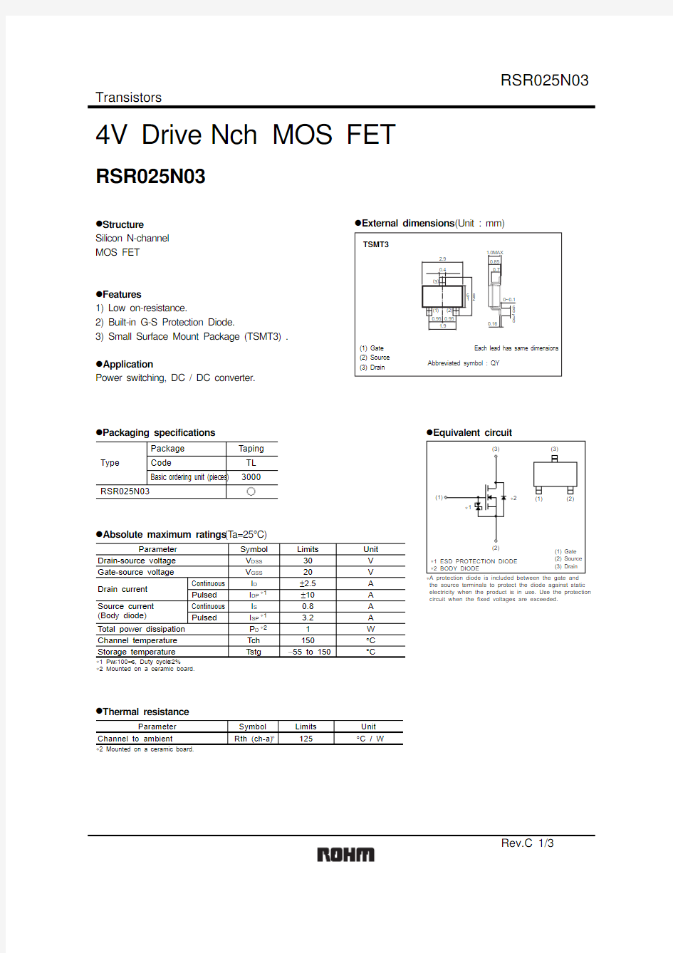
Power switching, DC / DC converter. z External dimensions (Unit : mm)
z Packaging specifications
z Absolute maximum ratings (T a=25°C)
?1?1?2Parameter
V V DSS Symbol 30V V GSS
20A I D A I DP A I S A I SP W P D °C Tch 150°C
Tstg ?55 to 150Limits Unit Drain-source voltage Gate-source voltage Drain current Total power dissipation Channel temperature Storage temperature
Continuous Pulsed Continuous Source current (Body diode)
Pulsed
?1 Pw ≤100μs, Duty cycle ≤2%?2 Mounted on a ceramic board.
±2.5±100.83.21
z Equivalent circuit
the source terminals to protect the diode against static electricity when the product is in use. Use the protection circuit when the fixed voltages are exceeded.
z Thermal resistance
°C / W
Rth (ch-a)125Parameter
Symbol Limits Unit Channel to ambient
?2 Mounted on a ceramic board.
?
Transistors
Rev.C 2/3
z Electrical characteristics (T a=25°C)
z Body diode characteristics (Source-Drain) (T a=25°C)
Forward voltage
V SD ?? 1.2V I S =3.2A, V GS =0V
Parameter
Symbol Min.Typ.
Max.Unit Conditions
?Pulsed
?
Transistors
Rev.C 3/3
z Electrical characteristic curves
DRAIN-SOURCE VOLTAGE : V DS (V)10100
C A P A C I T A N C E : C (p F )
1000
Fig.1 Typical Capacitance
vs. Drain-Source Voltage
DRAIN CURRENT : I D (A)S W I T C H I N G T I M E : t (n s )
Fig.2 Switching Characteristics
TOTAL GATE CHARGE : Qg (nC)
G A T E -S O U R C E V O L T A G E : V G S (V )
Fig.3 Dynamic Input Characteristics
GATE-SOURCE VOLTAGE : V GS (V)D R A I N C U R R E N T : I D (A )
Fig.4 Typical Transfer Characteristics
GATE-SOURCE VOLTAGE : V GS (V)S T A T I C D R A I N -S O U R C E O N -S T A T E R E S I S T A N C E : R D S (o n ) (m ?)
Fig.5 Static Drain-Source
On-State Resistance vs.
Gate-Source Voltage
SOURCE-DRAIN VOLTAGE : V SD (V)
S O U R C E C U R R E N T : I s (A )
Fig.6 Source Current vs.
Source-Drain Voltage
DRAIN CURRENT : I D (A)
S T A T I C D R A I N -S O U R C E O N -S T A T E R E S I S T A N C E : R D S (o n ) (m ?)
Fig.7 Static Drain-Source
On-State Resistance vs. Drain Current (Ι)
DRAIN CURRENT : I
D (A)S T A T I C D R A I N -S O U R C
E O N -S T A T E R E S I S T A N C E : R D S (o n ) (m ?)
Fig.8 Static Drain-Source
On-State Resistance vs. Drain Current (ΙΙ)
DRAIN CURRENT : I
D (A)
S T A T I C D R A I N -S O U R C E O N -S T A T E R E S I S T A N C E : R D S (o n ) (m ?)
Fig.9 Static Drain-Source
On-State Resistance vs. Drain Current (ΙΙΙ)
Appendix
About Export Control Order in Japan
Products described herein are the objects of controlled goods in Annex 1 (Item 16) of Export T rade Control
Order in Japan.
In case of export from Japan, please confirm if it applies to "objective" criteria or an "informed" (by MITI clause)
on the basis of "catch all controls for Non-Proliferation of Weapons of Mass Destruction.
Appendix1-Rev1.1