
4Ω Switch Connection between Two Ports
Minimal Propagation Delay through the Switch Low I CC
Zero Bounce in Flow-through Mode
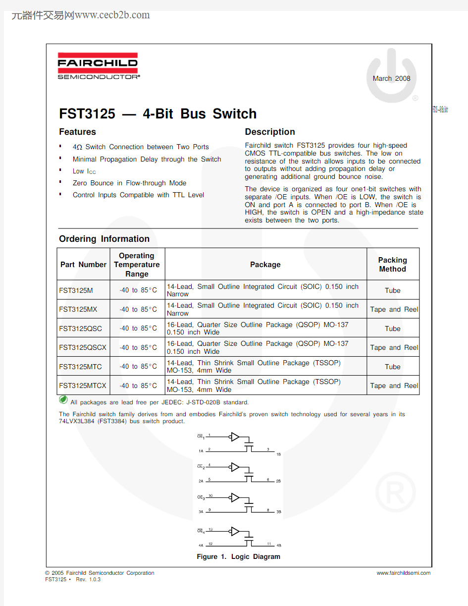
Control Inputs Compatible with TTL Level Fairchild switch FST3125 provides four high-speed CMOS TTL-compatible bus switches. The low on resistance of the switch allows inputs to be connected to outputs without adding propagation delay or generating additional ground bounce noise.
The device is organized as four one1-bit switches with separate /OE inputs. When /OE is LOW, the switch is ON and port A is connected to port B. When /OE is HIGH, the switch is OPEN and a high-impedance state exists between the two ports.
Ordering Information
Part Number
Operating
Temperature
Range
Package
Packing
Method
FST3125M -40 to 85°C 14-Lead, Small Outline Integrated Circuit (SOIC) 0.150 inch
Narrow
Tube
FST3125MX -40 to 85°C 14-Lead, Small Outline Integrated Circuit (SOIC) 0.150 inch
Narrow
Tape and Reel
FST3125QSC -40 to 85°C 16-Lead, Quarter Size Outline Package (QSOP) MO-137
0.150 inch Wide
Tube
FST3125QSCX -40 to 85°C 16-Lead, Quarter Size Outline Package (QSOP) MO-137
0.150 inch Wide
Tape and Reel
FST3125MTC -40 to 85°C 14-Lead, Thin Shrink Small Outline Package (TSSOP)
MO-153, 4mm Wide
Tube
FST3125MTCX -40 to 85°C 14-Lead, Thin Shrink Small Outline Package (TSSOP)
MO-153, 4mm Wide
Tape and Reel
All packages are lead free per JEDEC: J-STD-020B standard.
The Fairchild switch family derives from and embodies Fairchild’s proven switch technology used for several years in its 74LVX3L384 (FST3384) bus switch product.
Figure 1. Logic Diagram
FST3125 — 4-Bit Bus Switch
1A
1B
/OE 22A
2B GND
/OE 44A
4B
/OE 3
3A
3B
13
12
11109823
4
5
6
7
/OE 11A
1B /OE 2
2A
2B
GND /OE 44A
4B
/OE 33A
3B
NC
15
14
1312
11
10
923
45
6
7
8
Figure 2. SOIC and TSSOP Pin Assignments
Figure 3. QSOP Pin Assignments
Pin Descriptions
Pin Names
Description
/OE 1, /OE 2, /OE 3, /OE 4
Bus Switch Enables
1A, 2A, 3A, 4A Bus A 1B, 2B, 3B, 4B
Bus B
NC Not Connected
V CC Supply Voltage
GND Ground
Truth Table
Inputs
Inputs/Outputs
FST3125 — 4-Bit Bus Switch
Max.
Unit
Symbol Parameter Min.
Voltage -0.5 7.0 V
V CC Supply
V S DC Switch Voltage -0.5 7.0 V
V
7.0
V IN DC Input Voltage(1) -0.5
I IK DC Input Current -50 mA
I OUT DC Output Sink Current 128 mA
V CC / GND Current ±100 mA
I CC / I GND DC
T STG Storage Temperature Range -65 +150 °C
Note:
1. The input and output negative voltage ratings may be exceeded if the input and output diode current ratings are
observed.
Recommended Operating Conditions
The Recommended Operating Conditions table defines the conditions for actual device operation. Recommended
operating conditions are specified to ensure optimal performance to the datasheet specifications. Fairchild does not
recommend exceeding them or designing to Absolute Maximum Ratings.
Unit
Symbol Parameter Min.
Max.
V CC Power Supply Operating 4.0 5.5 V
Voltage 0 5.5 V
V IN Input
Voltage 0 5.5 V
V OUT Output
Switch Control Input(2) 0 5
ns/V
t r, t f Input Rise and Fall Time
Switch I/O 0 DC
T A Operating Temperature, Free Air -40 +85 °C
Note:
2. Unused control inputs must be held HIGH or LOW. They may not float.
FST3125 — 4-Bit Bus Switch
V IK Clamp Diode Voltage I IN = -18mA 4.5 -1.2 V V IH High-Level Input Voltage 4.0 to 5.5 2.0 V V IL Low-Level Input Voltage
4.0 to
5.5
0.8
V
I IN Input Leakage Current 0 ≤ V IN ≤ 5.5 5.5 ±1.0 μA
I OZ
Off-state Leakage Current
0 ≤ A, B ≤ V CC 5.5 ±1.0 μA V IN = 0V, I IN = 64mA
4.5 4 7 V IN = 0V, I IN = 30mA 4.5 4 7 V IN = 2.4V, I IN = 15mA 4.5 8 15 R ON Switch On Resistance (3)
V IN = 2.4V, I IN = 15mA 4.0
11
20
Ω
I CC Quiescent Supply Current V IN = V CC or GND,
I OUT = 0
5.5 3 μA ΔI CC
Increase in I CC per Input
One Input at 3.4V, Other Inputs at V CC or GND
5.5 2.5 mA
Note :
3. Measured by the voltage drop between A and B pins at the indicated current through the switch. On resistance
is determined by the lower of the voltages on the A or B pins.
AC Electrical Characteristics
T A = -40 to +85°C, C L = 50pF, and R U = R D = 500Ω.
V CC = 4.5 – 5.5V V CC = 4.0V
Symbol Parameter Conditions Min. Max. Min. Max.
Units Figure
t PHL , t PLH
Propagation Delay
Bus-to-Bus (4)
V IN = Open
0.25
0.25
ns
Figure 4Figure 5
t PZH ,t PZL
Output Enable Time
V IN = 7V for t PZL V IN = Open for t PZH
1.0 5.0 5.5 ns
Figure 4
Figure 5 t PHZ , t PLZ Output Disable Time
V IN = 7V for t PLZ V IN = Open for t PHZ
1.5 5.3 5.6 ns
Figure 4
Figure 5
Note :
4. This parameter is guaranteed by design, but is not tested. The bus switch contributes no propagation delay
other than the RC delay of the typical on resistance of the switch and the 50pF load capacitance when driven by an ideal voltage source (zero output impedance).
FST3125 — 4-Bit Bus Switch AC Loadings and Waveforms
Notes: Input driven by 50Ω source terminated in 50Ω.
C L includes load and stray capacitance.
Input PRR = 1.0MHz, t w = 500ns.
Figure 4. AC Test Circuit
Figure 5. AC Waveforms
LAND PATTERN RECOMMENDATION
NOTES: UNLESS OTHERWISE SPECIFIED
A) THIS PACKAGE CONFORMS TO JEDEC MS-012, VARIATION AB, ISSUE C,
B) ALL DIMENSIONS ARE IN MILLIMETERS.
C) DIMENSIONS DO NOT INCLUDE MOLD
FLASH OR BURRS.
D) LANDPATTERN STANDARD: SOIC127P600X145-14M
E) DRAWING CONFORMS TO ASME Y14.5M-1994
F) DRAWING FILE NAME: M14AREV13
PIN ONE INDICATOR
8°0°
SEATING PLANE
DETAIL A
SCALE: 20:1
GAGE PLANE 0.25
X 45°10.10C C
B C A
7
M
SEE DETAIL A
1.70 1.27
3.80
(0.33)
1.270.510.35
1.75 MAX
1.501.25
0.250.10
0.250.19
(1.04)
0.900.500.36R0.10
R0.100.500.25
Figure 6. 14-Lead, Small-Outline Integrated Circuit (SOIC) 0.150-inch Narrow
SIDE VIEW
TOP VIEW
DETAIL A
END VIEW
LAND PATTERN RECOMMENDATION
Figure 7. 16-Lead, Quarter-Size Outline Package (QSOP), MO-1370.150-inch Wide
C. DIMENSIONS ARE EXCLUSIVE OF BURRS, MOLD FLASH, AND TIE BAR EXTRUSIONS
F. DRAWING FILE NAME: MTC14REV6
R0.09 min
12.00°TOP & BOTTOM
1.00
D. DIMENSIONING AND TOLERANCES PER ANSI Y14.5M, 1982
R0.09min
E. LANDPATTERN STANDARD: SOP65P640X110-14M 6.10
1.65
0.45
A. CONFORMS TO JEDEC REGISTRATION MO-153, VARIATION AB, REF NOTE 6
B. DIMENSIONS ARE IN MILLIMETERS
Figure 8. 14-Lead, Thin Shrink Small Outline Package (TSSOP) MO-153, 4mm Wide
FST3125 — 4-Bit Bus Switch