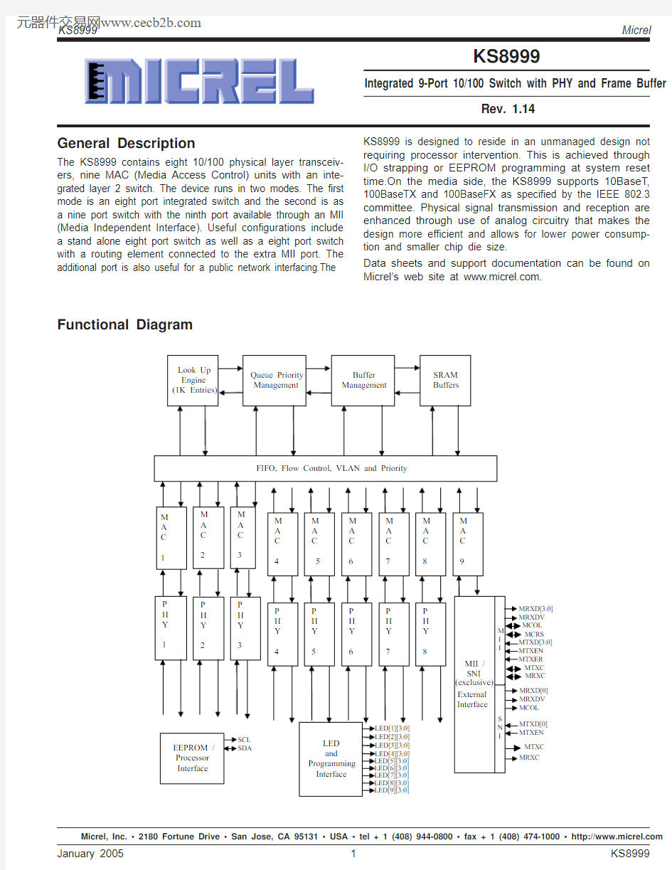
General Description
The KS8999 contains eight 10/100 physical layer transceiv-ers, nine MAC (Media Access Control) units with an inte-grated layer 2 switch. The device runs in two modes. The first
mode is an eight port integrated switch and the second is as a nine port switch with the ninth port available through an MII (Media Independent Interface). Useful configurations include a stand alone eight port switch as well as a eight port switch with a routing element connected to the extra MII port. The additional port is also useful for a public network interfacing.The
Micrel, Inc. ? 2180 Fortune Drive ? San Jose, CA 95131 ? USA ? tel + 1 (408) 944-0800 ? fax + 1 (408) 474-1000 ? https://www.doczj.com/doc/0612033703.html,
Functional Diagram
MRXC KS8999 is designed to reside in an unmanaged design not requiring processor intervention. This is achieved through I/O strapping or EEPROM programming at system reset time.On the media side, the KS8999 supports 10BaseT,100BaseTX and 100BaseFX as specified by the IEEE 802.3committee. Physical signal transmission and reception are enhanced through use of analog circuitry that makes the design more efficient and allows for lower power consump-tion and smaller chip die size.
Data sheets and support documentation can be found on Micrel’s web site at https://www.doczj.com/doc/0612033703.html,.
Features
?9 port (8+1) 10/100 integrated switch with eight physical layer transceivers and one MII/SNI interface ?Advanced Ethernet Switch with internal frame buffer –128K Byte of SRAM on chip for frame buffering
–2.0Gbps high performance memory bandwidth
–Wire speed reception and transmission
–Integrated address look-up engine, supports 1K absolute MAC addresses
–Automatic address learning, address aging and address migration
?Advanced Switch Features
–Supports 802.1p priority and port based priority
–Supports port based VLAN
–Supports 1536 byte frame for VLAN tag
–Supports DiffServ priority, 802.1p based priority or port based priorityo broadcast storm protection ?Proven transceiver technology for UTP and fiber operation
–10BaseT, 100BaseTX and 100BaseFX modes of operation
–Supports for UTP or fiber on all 8-ports
–Indicators for link, activity, full/half-duplex and speed –Hardware based 10/100, full/half, flow control and auto-negotiation
–Individual port forced modes (full duplex, 100BaseTX) when auto-negotiation is disabled
–Full duplex IEEE 802.3x flow control
–Half-duplex back pressure flow control
?Supports MDI/MDI-X auto crossover
?External MAC interface (MII or 7-wire) for router applications
?Unmanaged operation via strapping or EEPROM at system reset time (see Reset Reference Circuit section)?Comprehensive LED support
?Single 2.0V power supply with options for 2.5V and
3.3V I/O
?900 mA (1.80W) including physical transmit drivers ?Supports both commercial and industry temperature –Commercial temperature range:0°C to +70°C
(KS8999)
–Industrial temperature range:–40°C to +85°C
(KS8999I)
?Supports lead free products:
–Commercial temperature range: 0°C to +70°C
(KSZ8999)
–Industrial temperature range: –40°C to +85°C
(KSZ8999I)
?Available in 208-pin PQFP package Ordering Information
Part Number Temperature Range Package KS89990°C to +70°C208-Pin PQFP KS8999I–40°C to +85°C208-Pin PQFP KSZ89990°C to +70°C208-Pin PQFP KSZ8999I–40°C to +85°C208-Pin PQFP
Revision History
Revision Date Summary of Changes
1.0011/27/00Preliminary Release
1.0103/30/01Update maximum frame size
Update EEPROM priority descriptions
Update I/O pin definitionUpdate I/O descriptions
Update Electrical Characteristics
1.0204/20/01Correct timing information
1.0305/11/01Add MDI/MDI-X description
1.0406/22/01Change electrical requirements
1.050/6/25/01Correct I/O descriptions
1.0607/25/01Update PLL clock information
Update timing information
1.0708/09/01Correct LED[6][1:0] to float configuration
Add reverse and forward timing
Correct optional CPU timing
1.081/14/02Update Optional CPU interface
Correct I/O description for MCOL and MCRS
Correct pin 174 and 175 description
1.096/18/02Correct default to floating for pin 174
Change pin 87 TEST[3] to AUTOMDIX for enable/disable of auto MDI-MDIX function
1.102/27/03Add KS8999I industrial temperature
Update non-periodic blinking in Mode 1 of LED[1:9][0]
Add MRXD[0] description
1.115/12/03Changed Vcc from
2.00 to 2.10 (typical) Added FEF disable to T[4] pin #173
1.128/29/03Convert to new format.
1.131/19/05Correct pin type description. Correct selection of reference oscillator/crystal spec. Insert recommended
reset circuit.
1.141/31/05Added lead free and Industrial temperature packages.
Table of Contents
System Level Applications (6)
Pin Description (7)
I/O Grouping (13)
I/O Descriptions (13)
Pin Configuration (19)
Functional Overview:Physical Layer Transceiver (20)
100BaseTX Transmit (20)
100BaseTX Receive (20)
PLL Clock Synthesizer (20)
Scrambler/De-scrambler (100BaseTX only) (20)
100BaseFX Operation (20)
100BaseFX Signal Detection (20)
100BaseFX Far End Fault (20)
10BaseT Transmit (20)
10BaseT Receive (20)
Power Management (21)
Power Save Mode (21)
MDI/MDI-X Auto Crossover (21)
Auto-Negotiation (21)
Functional Overview:Switch Core (22)
Address Look-Up (22)
Learning (22)
Migration (22)
Aging (22)
Forwarding (22)
Switching Engine (22)
MAC Operation (22)
Inter Packet Gap (IPG) (22)
Backoff Algorithm (23)
Late Collision (23)
Illegal Frames (23)
Flow Control (23)
Half-Duplex Back Pressure (23)
Broadcast Storm Protection (23)
MII Interface Operation (24)
SNI Interface (7-wire) Operation (26)
Prorammable Features (26)
Priority Schemes (26)
Per Port Method (26)
802.1p Method (26)
IPv4 DSCP Method (26)
Other Priority Considerations (26)
VLAN Operation (27)
Station MAC Address (27)
EEPROM Operation (28)
Optional CPU Interface (28)
EEPROM Memory Map (29)
General Conrol Register (29)
Priority Classification Control:802.1p Tag Field (29)
Port 1 Control Register (29)
Port 2 Control Register (30)
Port 3 Control Register (30)
Port 4 Control Register (30)
Port 5 Control Register (31)
Port 6 Control Register (31)
Port 7 Control Register (32)
Port 8 Control Register (32)
Port 9 Control Register (32)
Port 1 VLAN Mask Register (33)
Port 2 VLAN Mask Register (33)
Port 3 VLAN Mask Register (34)
Port 4 VLAN Mask Register (34)
Port 5 VLAN Mask Register (35)
Port 6 VLAN Mask Register (35)
Port 7 VLAN Mask Register (36)
Port 8 VLAN Mask Register (36)
Port 9 VLAN Mask Register (37)
Port 1 VLAN Tag Insertion Value Registers (37)
Port 2 VLAN Tag Insertion Value Registers (37)
Port 3 VLAN Tag Insertion Value Registers (37)
Port 4 VLAN Tag Insertion Value Registers (37)
Port 5 VLAN Tag Insertion Value Registers (38)
Port 6 VLAN Tag Insertion Value Registers (38)
Port 7 VLAN Tag Insertion Value Registers (38)
Port 8 VLAN Tag Insertion Value Registers (38)
Port 9 VLAN Tag Insertion Value Registers (38)
Diff Serve Code Point Registers (38)
Station MAC Address Registers (38)
Absolute Maximum Ratings (39)
Operating Ratings (39)
Electrical Characteristics (KS8999) (39)
Electrical Characteristics (KS8999I) (41)
Timing Diagrams (42)
Reference Circuit (47)
4B/5B Coding (49)
MLT Coding (50)
MAC Frame (50)
Selection of Isolation Transformers (51)
Selection of Reference Oscillator/Crystal (51)
Qualified Magnetic Lists (51)
Package Information (52)
System Level Applications
The KS8999 can be configured to fit either in an eight port 10/
100 application or as a nine port 10/100 network interface with an extra MII/7-wire port. This MII/7-wire port can be connected to an external processor and used for routing
purposes or public network access. The major benefits of using the KS8999 are the lower power consumption,unmanaged operation, flexible configuration, built in frame buffering, VLAN abilities and traffic priority control. Two such applications are depicted below.
Or
MII or SNI
Figure 1.System Applicastions
Pin Description
Pin Number Pin Name Type(Note 1)Port Pin Function
1VDD_RX Pwr 2.0V for equalizer
2GND_RX GND Ground for equalizer
3GND_RX GND Ground for equalizer
4VDD_RX Pwr 2.0V for equalizer
5RXP[3]I3Physical receive signal + (differential)
6RXM[3]I3Physical receive signal - (differential)
7AOUT2O Factory test output
8DOUT2O Factory test output
9TXP[3]O3Physical transmit signal + (differential)
10TXM[3]O3Physical transmit signal - (differential)
11QH[5]Opd Factory test pin – leave open for normal operation 12QH[4]Opd Factory test pin – leave open for normal operation 13QH[3]Opd Factory test pin – leave open for normal operation 14QH[2]Opd Factory test pin – leave open for normal operation 15GND_TX GND Ground for transmit circuitry
16VDD_TX Pwr 2.0V for transmit circuitry
17VDD_TX Pwr 2.0V for transmit circuitry
18GND-ISO GND Analog ground
19TXP[4]O4Physical transmit signal + (differential)
20TXM[4]O4Physical transmit signal - (differential)
21GND_TX GND Ground for transmit circuitry
22RXP[4]I4Physical receive signal + (differential)
23RXM[4]I4Physical receive signal - (differential)
24GND_RX GND Ground for equalizer
25VDD_RX Pwr 2.0V for equalizer
26ISET Set physical transmit output current
27GND-ISO GND Analog ground
28VDD_RX Pwr 2.0V for equalizer
29GND_RX GND Ground for equalizer
30RXP[5]I5Physical receive signal + (differential)
31RXM[5]I5Physical receive signal - (differential)
32GND_TX GND Ground for transmit circuitry
33TXP[5]O5Physical transmit signal + (differential)
34TXM[5]O5Physical transmit signal - (differential)
Note 1.Pwr = power supply
GND = ground
I = input
O = output
I/O = bi-directional
Ipu = input w/ internal pull-up
Ipd = input w/ internal pull-down
Opu = output w/ internal pull-up
Opd = output w/ internal pull-down
Ipd/O = input w/ internal pull-down during reset, output pin otherwise
Ipu/O = input w/ internal pull-up during reset, output pin otherwise
Pin Number Pin Name Type(Note 1)Port Pin Function
35GND-ISO GND Analog ground
36VDD_TX Pwr 2.0V for transmit circuitry
37VDD_TX Pwr 2.0V for transmit circuitry
38GND_TX GND Ground for transmit circuitry
39QL[2]Opd Factory test pin – leave open for normal operation 40QL[3]Opd Factory test pin – leave open for normal operation 41QL[4]Opd Factory test pin – leave open for normal operation 42QL[5]Opd Factory test pin – leave open for normal operation 43TXP[6]O6Physical transmit signal + (differential)
44TXM[6]O6Physical transmit signal - (differential)
45DOUT O Factory test output – leave open for normal operation 46AOUT O Factory test output – leave open for normal operation 47RXP[6]I6Physical receive signal + (differential)
48RXM[6]I6Physical receive signal - (differential)
49VDD_RX Pwr 2.0V for equalizer
50GND_RX GND Ground for equalizer
51GND_RX GND Ground for equalizer
52VDD_RX Pwr 2.0V for equalizer
53GND-ISO GND Analog ground
54RXP[7]I7Physical receive signal + (differential)
55RXM[7]I7Physical receive signal - (differential)
56GND_TX GND Ground for transmit circuitry
57TXP[7]O7Physical transmit signal + (differential)
58TXM[7]O7Physical transmit signal - (differential)
59VDD_TX Pwr 2.0V for transmit circuitry
60VDD_TX Pwr 2.0V for transmit circuitry
61TXP[8]O8Physical transmit signal + (differential)
62TXM[8]O8Physical transmit signal - (differential)
63GND_TX GND Ground for transmit circuitry
64RXP[8]I8Physical receive signal + (differential)
65RXM[8]I8Physical receive signal - (differential)
66GND_RX GND Ground for equalizer
67VDD_RX Pwr 2.0V for equalizer
68FXSD[5]Ipd5Fiber signal detect
69FXSD[6]Ipd6Fiber signal detect
Note 1.Pwr = power supply
GND = ground
I = input
O = output
I/O = bi-directional
Ipu = input w/ internal pull-up
Ipd = input w/ internal pull-down
Opu = output w/ internal pull-up
Opd = output w/ internal pull-down
Ipd/O = input w/ internal pull-down during reset, output pin otherwise
Ipu/O = input w/ internal pull-up during reset, output pin otherwise
Pin Number Pin Name Type(Note 1)Port Pin Function
70FXSD[7]Ipd7Fiber signal detect
71FXSD[8]Ipd8Fiber signal detect
72GND_RCV GND Ground for clock recovery circuit
73GND_RCV GND Ground for clock recovery circuit
74VDD_RCV Pwr 2.0V for clock recovery circuit
75VDD_RCV Pwr 2.0V for clock recovery circuit
76GND_RCV GND Ground for clock recovery circuit
77GND_RCV GND Ground for clock recovery circuit
78VDD_RCV Pwr 2.0V for clock recovery circuit
79VDD_RCV Pwr 2.0V for clock recovery circuit
80BTOUT2O Factory test pin – leave open for normal operation
81CTOUT2O Factory test pin – leave open for normal operation
82RLPBK I Enable loop back for testing – pull-down/float for normal operation 83MUX[1]I Factory test pin – float for normal operation
84MUX[2]I Factory test pin – float for normal operation
85TEST[1]I Factory test pin – float for normal operation
86TEST[2]I Factory test pin – float for normal operation
87AUTOMDIX I Auto MDI/MDIX enable and disable – pull-up/float enable; pull-down
disable
88T[1]Ipu Factory test pin – float for normal operation
89T[2]Ipd Factory test pin – float for normal operation
90T[3]Ipd Factory test pin – float for normal operation
91EN1P Ipd Enable 802.1p for all ports
92SDA Ipd/O Serial data from EEPROM or processor
93SCL Ipd/O Clock for EEPROM or from processor
94VDD Pwr 2.0V for core digital circuitry
95GND GND Ground for digital circuitry
96MTXEN Ipd9MII transmit enable
97MTXD[3]Ipd9MII transmit bit 3
98MTXD[2]Ipd9MII transmit bit 2
99MTXD[1]Ipd9MII transmit bit 1
100MTXD[0]Ipd9MII transmit bit 0
101MTXER Ipd9MII transmit error
102MTXC Ipd/O9MII transmit clock
103MCOL Ipd/O9MII collision detected
104MCRS Ipd/O9MII carrier sense
Note 1.Pwr = power supply
GND = ground
I = input
O = output
I/O = bi-directional
Ipu = input w/ internal pull-up
Ipd = input w/ internal pull-down
Opu = output w/ internal pull-up
Opd = output w/ internal pull-down
Ipd/O = input w/ internal pull-down during reset, output pin otherwise
Ipu/O = input w/ internal pull-up during reset, output pin otherwise
Pin Number Pin Name Type(Note 1)Port Pin Function
105VDD-IO Pwr 2.0V, 2.5V or 3.3V for I/O circuitry
106GND GND Ground for digital circuitry
107GND GND Ground for digital circuitry
108VDD Pwr 2.0V for core digital circuitry
109BIST Ipd Built in self test – tie low for normal operation 110RST#I Reset – active low
111LED[1][3]Ipu/O1LED indicator 3
112LED[1][2]Ipu/O1LED indicator 2
113LED[1][1]Ipu/O1LED indicator 1
114LED[1][0]Ipu/O1LED indicator 0
115LED[2][3]Ipu/O2LED indicator 3
116LED[2][2]Ipu/O2LED indicator 2
117LED[2][1]Ipu/O2LED indicator 1
118LED[2][0]Ipu/O2LED indicator 0
119MRXDV Opd9MII receive data valid
120MRXD[3]Opu9MII receive bit 3
121MRXD[2]Opu9MII receive bit 2
122MRXD[1]Opu9MII receive bit 1
123MRXD[0]Opu9MII receive bit 0
124MRXC Ipu/O9MII receive clock
125VDD-IO Pwr 2.0V, 2.5V or 3.3V for I/O circuitry
126GND GND Ground for digital circuitry
127LED[3][3]Ipu/O3LED indicator 3
128LED[3][2]Ipu/O3LED indicator 2
129LED[3][1]Ipu/O3LED indicator 1
130LED[3][0]Ipu/O3LED indicator 0
131LED[4][3]Ipu/O4LED indicator 3
132LED[4][2]Ipu/O4LED indicator 2
133LED[4][1]Ipu/O4LED indicator 1
134LED[4][0]Ipu/O4LED indicator 0
135VDD Pwr 2.0V for core digital circuitry
136GND GND Ground for digital circuitry
137LED[5][3]Ipu/O5LED indicator 3
138LED[5][2]Ipu/O5LED indicator 2
139LED[5][1]Ipu/O5LED indicator 1
Note 1.Pwr = power supply
GND = ground
I = input
O = output
I/O = bi-directional
Ipu = input w/ internal pull-up
Ipd = input w/ internal pull-down
Opu = output w/ internal pull-up
Opd = output w/ internal pull-down
Ipd/O = input w/ internal pull-down during reset, output pin otherwise
Ipu/O = input w/ internal pull-up during reset, output pin otherwise
Pin Number Pin Name Type(Note 1)Port Pin Function
140LED[5][0]Ipu/O5LED indicator 0
141LED[6][3]Ipu/O6LED indicator 3
142LED[6][2]Ipu/O6LED indicator 2
143LED[6][1]Ipu/O6LED indicator 1
144LED[6][0]Ipu/O6LED indicator 0
145LED[7][3]Ipu/O7LED indicator 3
146LED[7][2]Ipu/O7LED indicator 2
147LED[7][1]Ipu/O7LED indicator 1
148VDD-IO Pwr 2.0V, 2.5V or 3.3V for I/O circuitry
149LED[7][0]Ipu/O7LED indicator 0
150LED[8][3]Ipu/O8LED indicator 3
151LED[8][2]Ipu/O8LED indicator 2
152LED[8][1]Ipu/O8LED indicator 1
153LED[8][0]Ipu/O8LED indicator 0
154GND GND Ground for digital circuitry
155GND GND Ground for digital circuitry
156IO_SWM Ipu Factory test pin – tie high for normal operation
157VDD Pwr 2.0V for core digital circuitry
158LED[9][3]Ipu/O9LED indicator 3
159LED[9][2]Ipu/O9LED indicator 2
160LED[9][1]Ipu/O9LED indicator 1
161LED[9][0]Ipu/O9LED indicator 0
162MIIS[1]Ipd9MII mode select bit 1
163MIIS[0]Ipd9MII mode select bit 0
164MODESEL[3]Ipd Selects LED and test modes
165MODESEL[2]Ipd Selects LED and test modes
166MODESEL[1]Ipd Selects LED and test modes
167MODESEL[0]Ipd Selects LED and test modes
168TESTEN Ipd Factory test pin – tie low for normal operation
169SCANEN Ipd Factory test pin – tie low for normal operation
170PRSV Ipd Reserve 6KB buffer for priority frames
171CFGMODE Ipu Configures programming interface for EEPROM or processor 172T[5]I Factory test pin – float for normal operation
173T[4]Ipdthevillage F/D = normal operation (default)
U = disable FEF
174Reserve I Reserved – floating for normal operation
Note 1.Pwr = power supply
GND = ground
I = input
O = output
I/O = bi-directional
Ipu = input w/ internal pull-up
Ipd = input w/ internal pull-down
Opu = output w/ internal pull-up
Opd = output w/ internal pull-down
Ipd/O = input w/ internal pull-down during reset, output pin otherwise
Ipu/O = input w/ internal pull-up during reset, output pin otherwise
Pin Number Pin Name Type(Note 1)Port Pin Function
175Reserve I Reserved - floating for normal operation
176X1I Crystal or clock input
177X2O Connect to crystal
178VDD_PLLTX Pwr 2.0 V for phase locked loop circuit
179GND_PLLTX GND Ground for phase locked loop circuit
180CTOUT O Factory test pin – leave open for normal operation 181BTOUT O Factory test pin – leave open for normal operation 182VDD_RCV Pwr 2.0V for clock recovery circuit
183VDD_RCV Pwr 2.0V for clock recovery circuit
184GND_RCV GND Ground for clock recovery circuit
185GND_RCV GND Ground for clock recovery circuit
186VDD_RCV Pwr 2.0V for clock recovery circuit
187VDD_RCV Pwr 2.0V for clock recovery circuit
188GND_RCV GND Ground for clock recovery circuit
189GND_RCV GND Ground for clock recovery circuit
190FXSD[1]Ipd1Fiber signal detect
191FXSD[2]Ipd2Fiber signal detect
192FXSD[3]Ipd3Fiber signal detect
193FXSD[4]Ipd4Fiber signal detect
194VDD_RX Pwr 2.0V for equalizer
195GND_RX GND Ground for equalizer
196RXP[1]I1Physical receive signal + (differential)
197RXM[1]I1Physical receive signal - (differential)
198GND_TX GND Ground for transmit circuitry
199TXP[1]O1Physical transmit signal + (differential)
200TXM[1]O1Physical transmit signal - (differential)
201VDD_TX Pwr 2.0V for transmit circuitry
202VDD_TX Pwr 2.0V for transmit circuitry
203TXP[2]O2Physical transmit signal + (differential)
204TXM[2]O2Physical transmit signal - (differential)
205GND_TX GND Ground for transmit circuitry
206RXP[2]I2Physical receive signal + (differential)
207RXM[2]I2Physical receive signal - (differential)
208GND-ISO GND Analog ground
Note 1.Pwr = power supply
GND = ground
I = input
O = output
I/O = bi-directional
Ipu = input w/ internal pull-up
Ipd = input w/ internal pull-down
Opu = output w/ internal pull-up
Opd = output w/ internal pull-down
Ipd/O = input w/ internal pull-down during reset, output pin otherwise
Ipu/O = input w/ internal pull-up during reset, output pin otherwise
I/O Grouping
Group Name Description
PHY Physical Interface
MII Media Independent Interface
SNI Serial Network Interface
IND LED Indicators
UP Unmanaged Programmable
CTRL Control and Miscellaneous
TEST Test (Factory)
PWR Power and Ground
I/O Descriptions
Group I/O Names Active Status Description
PHY RXP[1:8]Analog Differential inputs (receive) for connection to media (transformer or fiber module) RXM[1:8]
TXP[1:8]Analog Differential outputs (transmit) for connection to media (transformer or fiber module)
TXM[1:8]
FXSD[1:8]H Fiber signal detect – connect to fiber signal detect output on fiber module with
appropriate voltage divider if needed. Tie low for copper mode.
ISET Analog Transmit Current Set. Connecting an external reference resistor to set transmitter
output current. This pin connects to a 3K? 1% resistor to ground if a transformer with
1:1 turn ratio is used.
MII MRXD[0:3]H Four bit wide data bus for receiving MAC frames
MRXDV H Receive data valid
MCOL H Receive collision detection
MCRS H Carrier sense
MTXD[0:3]H Four bit wide data bus for transmitting MAC frames
MTXEN H Transmit enable
MTXER H Transmit error
MRXC Clock MII receive clock
MTXC Clock MII transmit clock
SNI MTXD[0]H Serial transmit data
MTXEN H Transmit enable
MRXD[0]H Serial receive data
MRXDV H Receive carrier sense/data valid
MCOL H Collision detection
MRXC Clock SNI receive clock
MTXC Clock SNI transmit clock
IND LED[1:9][0]L Output (after reset)
Mode 0:Speed (on = 100/off = 10)
Mode 1:10/100 + link + activity
10Mb link activity = slow blink (non-periodic blinking)
100Mb link activity = fast blink (non-periodic blinking)
Mode 2:Collision (on = collision/off = no collision)
Mode 3:Speed (on = 100/off = 10)
Group I/O Names Active Status Description(Note 1)
LED[1:9][1]L Output (after reset)
Mode 0:Full Duplex (on = full/off = half)
Mode 1:Full Duplex (on = full/off = half)
Mode 2:Full Duplex (on = full/off = half)
Mode 3:Reserved
LED[1:9][2]L Output (after reset)
Mode 0:Collision (on = collision/off = no collision)
Mode 1:Transmit Activity (on during transmission)
Mode 2:Link activity (10Mb mode)
Mode 3:Full Duplex + Collision
(constant on = full duplex;intermittent on = collision;off = half-duplex with no collision) LED[1:9][3]L Output (after reset)
Mode 0:Link + Activity
When LED is solid “on”, it indicates the link is on for both 10 or 100BaseTX, but no
data is transmitting or receiving.
When LED is solid “off”, it indicates the link is off.
When LED is blinking, it indicates data is transmitting or receiving for either 10 or 100
BaseTX
Mode 1:Receive Activity (on = receiving/off = not receiving)
Mode 2:Link activity (100Mb mode)
Mode 3:Link + Activity (see description above)
Note:Mode is set by MODESEL[3:0] ; please see description in UP (unmanaged
programming) section.
UP MODESEL[3:0]H Mode select at reset time. LED mode is selected by using the table below. Note that
under normal operation MODESEL[3:2] must be tied low.
MODESEL
3210Operation
0000LED mode 0
0001LED mode 1
0010LED mode 2
0011LED mode 3
0100Used for factory testing
0101Used for factory testing
0110Used for factory testing
0111Used for factory testing
1000Used for factory testing
1001Used for factory testing
1010Used for factory testing
1011Used for factory testing
1100Used for factory testing
1101Used for factory testing
1110Used for factory testing
1111Used for factory testing
LED[1][3]Programs auto-negotiation on port 1
D = Disable auto-negotiation, F/U = Enable auto-negotiation (default)
LED[1][2]Programs auto-negotiation on port 2
D = Disable auto-negotiation, F/U = Enable auto-negotiation (default)
LED[1][1]Programs auto-negotiation on port 3
D = Disable auto-negotiation, F/U = Enable auto-negotiation (default)
Note 1.All unmanaged programming takes place at reset time only. For unmanaged programming:F = Float, D = Pull-down, U = Pull-up.
See “Reference Circuits” section.
Group I/O Names Active Status Description(Note 1)
LED[1][0]Programs auto-negotiation on port 4
D = Disable auto-negotiation, F/U = Enable auto-negotiation (default)
LED[2][3]Programs auto-negotiation on port 5
D = Disable auto-negotiation, F/U = Enable auto-negotiation (default)
LED[2][2]Programs auto-negotiation on port 6
D = Disable auto-negotiation, F/U = Enable auto-negotiation (default)
LED[2][1]Programs auto-negotiation on port 7
D = Disable auto-negotiation, F/U = Enable auto-negotiation (default)
LED[2][0]Programs auto-negotiation on port 8
D = Disable auto-negotiation, F/U = Enable auto-negotiation (default)
LED[3][3]Programs port speed on port 1. This is only effective if auto-negotiation is disabled.
D = 10Mbps, F/U = 100Mbps (default)
LED[3][2]Programs port speed on port 2. This is only effective if auto-negotiation is disabled.
D = 10Mbps, F/U = 100Mbps (default)
LED[3][1]Programs port speed on port 3. This is only effective if auto-negotiation is disabled.
D = 10Mbps, F/U = 100Mbps (default)
LED[3][0]Programs port speed on port 4. This is only effective if auto-negotiation is disabled.
D = 10Mbps, F/U = 100Mbps (default)
LED[4][3]Programs port speed on port 5. This is only effective if auto-negotiation is disabled.
D = 10Mbps, F/U = 100Mbps (default)
LED[4][2]Programs port speed on port 6. This is only effective if auto-negotiation is disabled.
D = 10Mbps, F/U = 100Mbps (default)
LED[4][1]Programs port speed on port 7. This is only effective if auto-negotiation is disabled.
D = 10Mbps, F/U = 100Mbps (default)
LED[4][0]Programs port speed on port 8. This is only effective if auto-negotiation is disabled.
D = 10Mbps, F/U = 100Mbps (default)
LED[5][3]Programs port duplex (full/ half) on port 1. This is only effective if auto-negotiation is
disabled or if this end has auto- negotiation enabled and the far end has auto
negotiation disabled.
D = Full-duplex, F/U = Half-duplex (default)
LED[5][2]Programs port duplex (full/ half) on port 2. This is only effective if auto-negotiation is
disabled or if this end has auto-negotiation enabled and the far end has auto-
negotiation disabled.
D = Full-duplex, F/U = Half-duplex (default)
LED[5][1]Programs port duplex (full/ half) on port 3. This is only effective if auto-negotiation is
disabled or if this end has auto-negotiation enabled and the far end has auto-
negotiation disabled.
D = Full-duplex, F/U = Half-duplex (default)
LED[5][0]Programs port duplex (full/ half) on port 4. This is only effective if auto-negotiation is
disabled or if this end has auto-negotiation enabled and the far end has auto-
negotiation disabled.
D = Full-duplex, F/U = Half-duplex (default)
LED[9][3]Programs port duplex (full/ half) on port 5. This is only effective if auto-negotiation is
disabled or if this end has auto-negotiation enabled and the far end has auto
negotiation disabled.
D = Full-duplex, F/U = Half-duplex (default)
LED[9][2]Programs port duplex (full/ half) on port 6. This is only effective if auto-negotiation is
disabled or if this end has auto-negotiation enabled and the far end has auto-
negotiation disabled.
D = Full-duplex, F/U = Half-duplex (default)
Note 1.All unmanaged programming takes place at reset time only. For unmanaged programming:F = Float, D = Pull-down, U = Pull-up.
See “Reference Circuits” section.
Group I/O Names Active Status Description(Note 1)
LED[9][1]Programs port duplex (full / half) on port 7. This is only effective if auto-negotiation is
disabled or if this end has auto-negotiation enabled and the far end has auto-
negotiation disabled.
D = Full-duplex, F/U = Half-duplex (default)
LED[9][0]Programs port duplex (full / half) on port 8. This is only effective if auto-negotiation is
disabled or if this end has auto-negotiation enabled and the far end has auto-
negotiation disabled.
D = Full-duplex, F/U = Half-duplex (default)
LED[6][3]Programs back-off aggressiveness for half-duplex mode
D = Less aggressive back-off, F/U = More aggressive back-off (default)
LED[6][2]Programs retries for frames that encounter collisions.
D = Drop frame after 16 collisions, F/U = Continue sending frame regardless of the
number of collisions (default)
LED[6][1:0]Reserved – use float configuration
LED[7][3]Programs flow control
D = No flow control, F/U = Flow control enabled (default)
LED[7][2]Programs broadcast storm protection.
D = 5% broadcast frames allowed, F/U = Unlimited broadcast frames (default)
LED[7][1]Programs buffer sharing feature.
D = Equal amount of buffers per port (113 buffers), F/U = Share buffers up to 512
buffers on a single port (default)
LED[7][0]Reserved – use float configuration
LED[8][3]Programs address aging.
D = Aging disabled, F/U = Enable 5 minute aging (default)
LED[8][2]Programs frame length enforcement.
D = Max length for VLAN is 1522 bytes and without VLAN is 1518 bytes
F/U = Max length is 1536 bytes (default)
LED[8][1]Reserved
LED[8][0]Programs half-duplex back pressure.
D = No half-duplex back pressure, F/U = Half-duplex back pressure enabled (default)
MRXD[3]Programs port 9 speed
D = 10Mbps, F/U = 100Mbps (default)
MRXD[2]Programs port 9 duplex
D = Half-duplex, F/U = Full duplex (default)
MRXD[1]Programs port 9 flow control
D = Flow control, F/U = No flow control (default)
MRXD[0] D = reserved, F/U = normal operation (default)
CTRL EN1P H Enable 802.1p for all ports – this enables QoS based on the priority field in the layer
2 header.
0 = 802.1p selected by port in EEPROM
1 = Use 802.1p priority field unless disabled in EEPROM
Note: This is also controlled by the EEPROM registers (registers 4-12 bit 4). The values
in the EEPROM supercede this pin. Also, if the priority selection is unaltered in the
EEPROM registers (register 3 bits 0-7) then values above 3 are considered high priorty
and less than 4 are low priority.
MIIS[1:0]H MII mode selection – allows the MII to run in the following modes
MIIS Operating mode
10
00Disable MII interface
01Reverse MII
10Forward MII
117 wire mode (SNI)
Note 1.All unmanaged programming takes place at reset time only. For unmanaged programming:F = Float, D = Pull-down, U = Pull-up.
See “Reference Circuits” section.
Group I/O Names Active Status Description(Note 1)
PRSV H Priority buffer reserve – reserves 6KB of buffer space for the priority traffic if enabled.
0 = No priority reserve
1 = Reserve 6KB for priority traffic
Note: This is also controlled by the EEPROM registers (register 2 bit 1). The value in
the EEPROM supercedes this pin.
CFGMODE H Selects between EEPROM or processor for programming interface.
0 = Processor interface
1 = EEPROM interface or not programmed on this interface (SCL / SDA not used)
X1Clock External crystal or clock input
X2Clock Used when other polarity of crystal is needed. This is unused for a normal clock input.
SCL Clock Clock for EEPROM
SDA I/O Serial data for EEPROM
RST#L System reset
TEST TESTEN H Factory test input – tie low for normal operation
SCANEN H Factory test input – tie low for normal operation
MUX[1:2]H Factory test input – leave open for normal operation
AOUT H Factory test output – leave open for normal operation
DOUT H Factory test output – leave open for normal operation
AOUT2H Factory test output – leave open for normal operation
DOUT2H Factory test output – leave open for normal operation
BTOUT H Factory test output – leave open for normal operation
CTOUT H Factory test output – leave open for normal operation
BTOUT2H Factory test output – leave open for normal operation
CTOUT2H Factory test output – leave open for normal operation
TEST[1:2]H Factory test inputs – leave open for normal operation
AUTOMDIX H F/U = Enable Auto MDI/MDIX (normal operation)
D = Disable Auto MDI/MDIX
T[1:3] & T[5]H Factory test inputs – leave open (float) for normal operation
T[4]H F/D = normal operation (default)
U = Disable FEF
QH[2:5]H Factory test outputs – leave open for normal operation
QL[2:5]H Factory test outputs – leave open for normal operation
IO_SWM H Factory test input – tie high for normal operation
RLPBK H Factory test input – tie low for normal operation
BIST H Factory test input – tie low for normal operation
PWR VDD_RX 2.0V for equalizer
GND_RX Ground for equalizer
VDD_TX 2.0V for transmit circuitry
GND_TX Ground for transmit circuitry
VDD_RCV 2.0V for clock recovery circuitry
GND_RCV Ground for clock recovery
VDD_PLLTX 2.0V for phase locked loop circuitry
Note 1.All unmanaged programming takes place at reset time only. For unmanaged programming:F = Float, D = Pull-down, U = Pull-up.
See “Reference Circuits” section.
Group I/O Names Active Status Description
GND_PLLTX Ground for phase locked loop circuitry
GND-ISO Analog ground
VDD 2.0V for core digital circuitry
VDD-IO 2.0V, 2.5V or 3.3V for I/O circuitry
GND Ground for digital circuitry
Pin Configuration
MCRS MCOL MTXC MTXER MTXD[0]MTXD[1]MTXD[2]MTXD[3]MTXEN GND VDD SCL SDA EN1P T[3]T[2]T[1]
AUTOMDIX TEST[2]TEST[1]MUX[2]MUX[1]RLPBK CTOUT2BTOUT2VDD_RCV VDD_RCV GND_RCV GND_RCV VDD_RCV VDD_RCV GND_RCV GND_RCV FXSD[8]FXSD[7]FXSD[6]FXSD[5]VDD_RX GND_RX RXM[8]RXP[8]GND_TX TXM[8]TXP[8]VDD_TX VDD_TX TXM[7]TXP[7]GND_TX RXM[7]RXP[7]GND_ISO
VDD LED[9][3]LED[9][2]LED[9][1]LED[9][0]MIIS[1]MIIS[0]MODESEL[3]MODESEL[2]MODESEL[1]MODESEL[0]
TESTEN SCANEN PRSV CFGMODE
T[5]T[4]
RESERVE RESERVE
X1X2
VDD_PLLTX GND_PLLTX
CTOUT BTOUT VDD_RCV VDD_RCV GND_RCV GND_RCV VDD_RCV VDD_RCV GND_RCV GND_RCV FXSD[1]FXSD[2]FXSD[3]FXSD[4]VDD_RX GND_RX RXP[1]RXM[1]GND_TX TXP[1]TXM[1]VDD_TX VDD_TX TXP[2]TXM[2]GND_TX RXP[2]RXM[2]GND_ISO
V D D _R X G N D _R X G N D _R X V D D _R X R X P [3]R X M [3]A O U T 2D O U T [2]T X P [3]T X M [3]Q H [5]Q H [4]Q H [3]Q H [2]G N D _T X V D D _T X V D D _T X G N D _I S O T X P [4]T X M [4]G N D _T X R X P [4]R X M [4]G N D _R X V D D _R X I S E T G N D _I S O V D D _R X G N D _R X R X P [5]R X M [5]G N D _T X T X P [5]T X M [5]G N D _I S O V D D _T X V D D _T X G N D _T X Q L [2]Q L [3]Q L [4]Q L [5]T X P [6]T X M [6]D O U T A O U T R X P [6]R X M [6]V D D _R X G N D _R X G N D _R X V D D _R X
I O _S W M
G N D G N D L E D [8][0]L E D [8][1]L E D [8][2]L E D [8][3]L E D [7][0]V D D _I O L E D [7][1]L E D [7][2]L E D [7][3]L E D [6][0]L E D [6][1]L E D [6][2]L E D [6][3]L E D [5][0]L E D [5][1]L E D [5][2]L E D [5][3]G N D V D D L E D [4][0]L E D [4][1]L E D [4][2]L E D [4][3]L E D [3][0]L E D [3][1]L E D [3][2]L E D [3][3]G N D V D D _I O M R X C M R X D [0]M R X D [1]M R X D [2]M R X D [3]M R X D V L E D [2][0]L E D [2][1]L E D [2][2]L E D [2][3]L E D [1][0]L E D [1][1]L E D [1][2]L E D [1][3]R S T #B I S T V D D G N D G N D V D D _I O
208-Pin PQFP (PQ)
Functional Overview:Physical Layer Transceiver
100BaseTX Transmit
The 100BaseTX transmit function performs parallel to serial conversion, 4B/5B coding, scrambling, NRZ to NRZI conver-sion, MLT3 encoding and transmission. The circuit starts with a parallel to serial conversion, which converts the data from the MAC into a 125MHz serial bit stream. The data and control stream is then converted into 4B/5B coding followed by a scrambler. The serialized data is further converted from NRZ to NRZI format, then transmitted in MLT3 current output. The output current is set by an external 1% 3.01k? resistor for the 1:1 transformer ratio. It has a typical rise/fall time of 4 ns and complies to the ANSI TP-PMD standard regarding amplitude balance, overshoot and timing jitters. The wave-shaped 10BaseT output is also incorporated into the 100BaseTX transmitter.
100BaseTX Receive
The 100BaseTX receiver function performs adaptive equalization, DC restoration, MLT3 to NRZI conversion, data and clock recovery, NRZI to NRZ conversion, de-scrambling, 4B/5B decoding and serial to parallel conversion. The receiving side starts with the equalization filter to compensate inter-symbol interference (ISI) over the twisted pair cable. Since the amplitude loss and phase distortion is a function of the length of the cable, the equalizer has to adjust its characteristics to optimize the performance. This is an ongoing process and can self adjust to the environmental changes such as tempera-ture variations. The equalized signal then goes through a DC restoration and data conversion block. The DC restoration circuit is used to compensate for the effect of base line wander and improve the dynamic range. The differential data conversion circuit converts the MLT3 format back to NRZI. The slicing threshold is also adaptive. The clock recovery circuit extracts the 125MHz clock from the edges of the NRZI signal. This recovered clock is then used to convert the NRZI signal into the NRZ format. The signal is then sent through the de-scrambler followed by the 4B/5B decoder. Finally, the NRZ serial data is provided as the input data to the MAC.
PLL Clock Synthesizer
The KS8999 generates 125MHz, 62.5MHz, 25MHz and 10MHz clocks for system timing. Internal clocks are generated from an external 25MHz crystal.
Scrambler/De-scrambler (100BaseTX only)
The purpose of the scrambler is to spread the power spectrum of the signal in order to reduce EMI and baseline wander. The data is scrambled by the use of an 11-bit wide linear feedback shift register (LFSR). This can generate a 2047-bit non-repetitive sequence. The receiver will then de-scramble the incoming data stream with the same sequence at the transmitter.
100BaseFX Operation
100BaseFX operation is very similar to 100BaseTX operation with the differences being that the scrambler/de-scrambler and MLT3 encoder/decoder are bypassed on transmission and reception. In this mode the auto-negotiation feature is bypassed since there is no standard that supports fiber auto-negotiation.
100BaseFX Signal Detection
The physical port runs in 100BaseFX mode if FXSDx >0.6V. FXSDx is considered ‘low’ when 0.6V
100BaseFX Far End Fault
Far end fault occurs when the signal detection is logically false from the receive fiber module which occurs when FXSDx is below 1.2V and above 0.6V. When this occurs, the transmission side signals the other end of the link by sending 84 1’s followed by a zero in the idle period between frames.
10BaseT Transmit
The output 10BaseT driver is incorporated into the 100BaseT driver to allow transmission with the same magnetics. They are internally wave-shaped and pre-emphasized into outputs with a typical 2.3V amplitude.
10BaseT Receive
On the receive side, input buffer and level detecting squelch circuits are employed. A differential input receiver circuit and a PLL perform the decoding function. The Manchester-encoded data stream is separated into clock signal and NRZ data. A squelch circuit rejects signals with levels less than 400mV or with short pulse widths in order to prevent noises at the RXP or RXM input from falsely triggering the decoder. When the input exceeds the squelch limit, the PLL locks onto the incoming signal and the KS8999 decodes a data frame. The receiver clock is maintained active during idle periods in between data reception.