
1
680412f
For more information www.linear .com/L TC6804-1
TYPICAL APPLICATION
FEATURES
DESCRIPTION
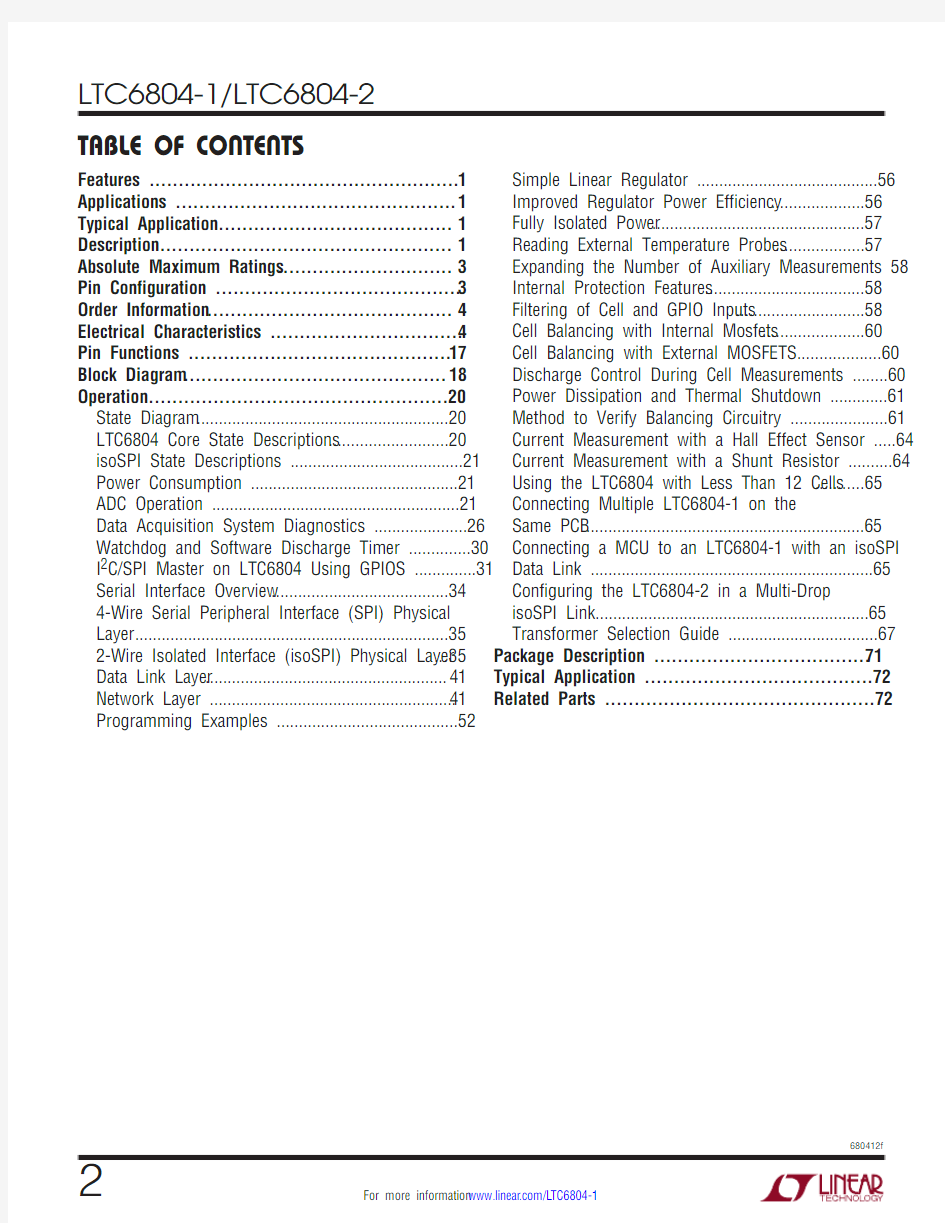
The L TC ?6804 is a 3rd generation multicell battery stack monitor that measures up to 12 series connected battery cells with a total measurement error of less than 1.2mV. The cell measurement range of 0V to 5V makes the LTC6804 suitable for most battery chemistries. All 12 cell voltages can be captured in 290μs, and lower data acquisition rates can be selected for high noise reduction.
Multiple LTC6804 devices can be connected in series, permitting simultaneous cell monitoring of long, high volt-age battery strings. Each LTC6804 has an isoSPI interface for high speed, RF-immune, local area communications. Using the LTC6804-1, multiple devices are connected in a daisy-chain with one host processor connection for all devices. Using the LTC6804-2, multiple devices are con-nected in parallel to the host processor, with each device individually addressed.
Additional features include passive balancing for each cell, an onboard 5V regulator, and 5 general purpose I/O lines. In sleep mode, current consumption is reduced to 4μA. The LTC6804 can be powered directly from the battery, or from an isolated supply.
L , L T, L TC , L TM, Linear Technology and the Linear logo are registered and isoSPI is a trademark of Linear Technology Corporation. All other trademarks are the property of their respective owners.
Total Measurement Error
vs Temperature of 5 Typical Units
APPLICATIONS
n
Measures Up to 12 Battery Cells in Series n Stackable Architecture Supports 100s of Cells n Built-In isoSPI? Interface:
1Mbps Isolated Serial Communications
Uses a Single T wisted Pair, Up to 100 Meters Low EMI Susceptibility and Emissions n 1.2mV Maximum Total Measurement Error n 290μs to Measure All Cells in a System
n Synchronized Voltage and Current Measurement n 16-Bit Delta-Sigma ADC with Frequency Programmable 3rd Order Noise Filter
n Engineered for ISO26262 Compliant Systems n Passive Cell Balancing with Programmable Timer n 5 General Purpose Digital I/O or Analog Inputs: Temperature or other Sensor Inputs Configurable as an I 2C or SPI Master n 4μA Sleep Mode Supply Current n 48-Lead SSOP Package
n
Electric and Hybrid Electric Vehicles n Backup Battery Systems
n
Grid Energy Storage
n
High Power Portable Equipment
12S1P
+
+
++
++
TEMPERATURE (°C)
M E A S U R E M E N T E R R O R (m V )
1.5
680412 TA01b
0–1.0–1.5–2.0
2.01.00.5–0.5
TABLE OF CONTENTS
Features (1)
Applications (1)
Typical Application (1)
Description (1)
Absolute Maximum Ratings (3)
Pin Configuration (3)
Order Information (4)
Electrical Characteristics (4)
Pin Functions (17)
Block Diagram (18)
Operation (20)
State Diagram (20)
LTC6804 Core State Descriptions (20)
isoSPI State Descriptions (21)
Power Consumption (21)
ADC Operation (21)
Data Acquisition System Diagnostics (26)
Watchdog and Software Discharge Timer (30)
I2C/SPI Master on LTC6804 Using GPIOS (31)
Serial Interface Overview (34)
4-Wire Serial Peripheral Interface (SPI) Physical Layer (35)
2-Wire Isolated Interface (isoSPI) Physical Layer (35)
Data Link Layer (41)
Network Layer (41)
Programming Examples (52)
Simple Linear Regulator (56)
Improved Regulator Power Efficiency (56)
Fully Isolated Power (57)
Reading External Temperature Probes (57)
Expanding the Number of Auxiliary Measurements 58 Internal Protection Features (58)
Filtering of Cell and GPIO Inputs (58)
Cell Balancing with Internal Mosfets (60)
Cell Balancing with External MOSFETS (60)
Discharge Control During Cell Measurements (60)
Power Dissipation and Thermal Shutdown (61)
Method to Verify Balancing Circuitry (61)
Current Measurement with a Hall Effect Sensor (64)
Current Measurement with a Shunt Resistor (64)
Using the LTC6804 with Less Than 12 Cells (65)
Connecting Multiple LTC6804-1 on the
Same PCB (65)
Connecting a MCU to an LTC6804-1 with an isoSPI Data Link (65)
Configuring the LTC6804-2 in a Multi-Drop isoSPI Link (65)
Transformer Selection Guide (67)
Package Description (71)
Typical Application (72)
Related Parts (72)
2680412f
For more information https://www.doczj.com/doc/0211123155.html,/L TC6804-1
3
680412f
For more information www.linear .com/L TC6804-1
ABSOLUTE MAXIMUM RATINGS
Total Supply Voltage V + to V –....................................75V Input Voltage (Relative to V –)
C0 .........................................................–0.3V to 0.3V C12 ........................................................–0.3V to 75V C(n) .....................................–0.3V to MIN (8 ? n, 75V) S(n) .....................................–0.3V to MIN (8 ? n, 75V) IPA, IMA, IPB, IMB ....................–0.3V to V REG + 0.3V DRIVE Pin ................................................–0.3V to 7V All Other Pins ...........................................–0.3V to 6V Voltage Between Inputs (Note 2)
C(n) to C(n – 1) ........................................–0.3V to 8V S(n) to C(n – 1) ........................................–0.3V to 8V C12 to C8 ...............................................–0.3V to 25V C8 to C4 .................................................–0.3V to 25V C4 to C0 .................................................–0.3V to 25V
(Note 1)
PIN CONFIGURATION
Current In/Out of Pins
All Pins Except V REG , IPA, IMA, IPB, IMB, S(n) ..10mA IPA, IMA, IPB, IMB .............................................30mA Operating Temperature Range
LTC6804I .............................................–40°C to 85°C LTC6804H ..........................................–40°C to 125°C Specified Temperature Range
LTC6804I .............................................–40°C to 85°C LTC6804H ..........................................–40°C to 125°C Junction Temperature ...........................................150°C Storage Temperature..............................–65°C to 150°C Lead Temperature (Soldering, 10sec)....................300°C
4
680412f
For more information www.linear .com/L TC6804-1
ORDER INFORMATION
ELECTRICAL CHARACTERISTICS
SYMBOL
PARAMETER
CONDITIONS
MIN TYP MAX UNITS ADC DC Specifications
Measurement Resolution l
0.1
mV/bit ADC Offset Voltage (Note 2)l 0.1mV ADC Gain Error
(Note 2)
l
0.01 0.02% %Total Measurement Error (TME) in Normal Mode
C(n) to C(n – 1), GPIO(n) to V – = 0±0.2mV
C(n) to C(n – 1) = 2.0
±0.1±0.8mV C(n) to C(n – 1), GPIO(n) to V – = 2.0l
±1.4mV C(n) to C(n – 1) = 3.3
±0.2±1.2mV C(n) to C(n – 1), GPIO(n) to V – = 3.3l ±2.2mV C(n) to C(n – 1) = 4.2
±0.3±1.6mV C(n) to C(n – 1), GPIO(n) to V – = 4.2l ±2.8mV C(n) to C(n – 1), GPIO(n) to V – = 5.0±1mV Sum of Cells
l ±0.2±0.75
%Internal Temperature, T = Maximum Specified Temperature ±5°C
V REG Pin l ±0.1±0.25%V REF2 Pin
l ±0.02±0.1%Digital Supply Voltage V REGD
l ±0.1
±1
%
The l denotes the specifications which apply over the full operating
temperature range, otherwise specifications are at T A = 25°C. The test conditions are V + = 39.6V, V REG = 5.0V unless otherwise noted.
LEAD FREE FINISH TAPE AND REEL PART MARKING*PACKAGE DESCRIPTION SPECIFIED TEMPERATURE RANGE LTC6804IG-1#PBF LTC6804IG-1#TRPBF LTC6804G-148-Lead Plastic SSOP –40°C to 85°C LTC6804HG-1#PBF LTC6804HG-1#TRPBF LTC6804G-148-Lead Plastic SSOP –40°C to 125°C LTC6804IG-2#PBF LTC6804IG-2#TRPBF LTC6804G-248-Lead Plastic SSOP –40°C to 85°C LTC6804HG-2#PBF
LTC6804HG-2#TRPBF
LTC6804G-2
48-Lead Plastic SSOP
–40°C to 125°C
Consult L TC Marketing for parts specified with wider operating temperature ranges. *The temperature grade is identified by a label on the shipping container. Consult L TC Marketing for information on nonstandard lead based finish parts.
For more information on lead free part marking, go to: https://www.doczj.com/doc/0211123155.html,/leadfree/
For more information on tape and reel specifications, go to: https://www.doczj.com/doc/0211123155.html,/tapeandreel/
ELECTRICAL CHARACTERISTICS
SYMBOL PARAMETER CONDITIONS MIN TYP MAX UNITS
Total Measurement Error (TME) in Filtered Mode C(n) to C(n – 1), GPIO(n) to V– = 0±0.1mV C(n) to C(n – 1) = 2.0±0.1±0.8mV C(n) to C(n – 1), GPIO(n) to V– = 2.0l±1.4mV C(n) to C(n – 1) = 3.3±0.2±1.2mV C(n) to C(n – 1), GPIO(n) to V– = 3.3l±2.2mV C(n) to C(n – 1) = 4.2±0.3±1.6mV C(n) to C(n – 1), GPIO(n) to V– = 4.2l±2.8mV C(n) to C(n – 1), GPIO(n) to V– = 5.0±1mV Sum of Cells l±0.2±0.75% Internal Temperature, T = Maximum
Specified Temperature
±5°C V REG Pin l±0.1±0.25% V REF2 Pin l±0.02±0.1% Digital Supply Voltage V REGD l±0.1±1%
Total Measurement Error (TME) in Fast Mode C(n) to C(n – 1), GPIO(n) to V– = 0±2mV C(n) to C(n – 1), GPIO(n) to V– = 2.0l±4mV C(n) to C(n – 1), GPIO(n) to V– = 3.3l±4.7mV C(n) to C(n – 1), GPIO(n) to V– = 4.2l±8.3mV C(n) to C(n – 1), GPIO(n) to V– = 5.0±10mV Sum of Cells l±0.3±1% Internal Temperature, T = Maximum
Specified Temperature
±5°C V REG Pin l±0.3±1% V REF2 Pin l±0.1±0.25% Digital Supply Voltage V REGD l±0.2±2%
Input Range C(n), n = 1 to 12l C(n – 1)C(n – 1) + 5V
C0l0
GPIO(n), n = 1 to 5l05V
I L Input Leakage Current When Inputs
Are Not Being Measured C(n), n = 0 to 12l10±250nA GPIO(n), n = 1 to 5l10±250nA
Input Current When Inputs Are Being Measured C(n), n = 0 to 12±2μA GPIO(n), n = 1 to 5±2μA
Input Current During Open Wire Detection
l70100130μA The l denotes the specifications which apply over the full operating
temperature range, otherwise specifications are at T A = 25°C. The test conditions are V+ = 39.6V, V REG = 5.0V unless otherwise noted.
5680412f
For more information https://www.doczj.com/doc/0211123155.html,/L TC6804-1
ELECTRICAL CHARACTERISTICS
SYMBOL PARAMETER CONDITIONS MIN TYP MAX UNITS
I VP V+ Supply Current
(See Figure 1: LTC6804 Operation
State Diagram)State: Core = SLEEP, isoSPI = IDLE V REG = 0V 3.86μA
V REG = 0V l 3.810μA
V REG = 5V 1.63μA
V REG = 5V l 1.65μA State: Core = STANDBY183250μA
l103260μA State: Core = REFUP or MEASURE 0.40.550.7mA
l0.3750.550.725mA
I REG(CORE)V REG Supply Current
(See Figure 1: LTC6804 Operation
State diagram)State: Core = SLEEP, isoSPI = IDLE V REG = 5V 2.24μA
V REG = 5V l 2.26μA State: Core = STANDBY103560μA
l63565μA State: Core = REFUP0.20.450.7mA
l0.150.450.75mA State: Core = MEASURE10.811.512.2mA
l10.711.512.3mA
I REG(isoSPI)Additional V REG Supply Current if
isoSPI in READY/ACTIVE States
Note: ACTIVE State Current
Assumes t CLK = 1μs, (Note 3)LTC6804-2: ISOMD = 1,
R B1 + R B2 = 2k
READY l 3.9 4.8 5.8mA
ACTIVE l 5.1 6.17.3mA LTC6804-1: ISOMD = 0,
R B1 + R B2 = 2k
READY l 3.7 4.6 5.6mA
ACTIVE l 5.7 6.88.1mA LTC6804-1: ISOMD = 1,
R B1 + R B2 = 2k
READY l 6.57.89.5mA
ACTIVE l10.211.313.3mA LTC6804-2: ISOMD = 1,
R B1 + R B2 = 20k
READY l 1.3 2.13mA
ACTIVE l 1.6 2.5 3.5mA LTC6804-1: ISOMD = 0,
R B1 + R B2 = 20k
READY l 1.1 1.9 2.8mA
ACTIVE l 1.5 2.3 3.3mA LTC6804-1: ISOMD = 1,
R B1 + R B2 = 20k
READY l 2.1 3.3 4.9mA
ACTIVE l 2.7 4.1 5.8mA The l denotes the specifications which apply over the full operating
temperature range, otherwise specifications are at T A = 25°C. The test conditions are V+ = 39.6V, V REG = 5.0V unless otherwise noted.
6680412f
For more information https://www.doczj.com/doc/0211123155.html,/L TC6804-1
ELECTRICAL CHARACTERISTICS
t CYCLE (Figure 3)Measurement + Calibration Cycle
Time When Starting from the
REFUP State in Normal Mode
Measure 12 Cells l212023352480μs
Measure 2 Cells l365405430μs
Measure 12 Cells and 2 GPIO Inputs l284531333325μs Measurement + Calibration Cycle
Time When Starting from the
REFUP State in Filtered Mode
Measure 12 Cells l183201.3213.5ms
Measure 2 Cells l30.5433.635.64ms
Measure 12 Cells and 2 GPIO Inputs l244268.4284.7ms Measurement + Calibration Cycle
Time When Starting from the
REFUP State in Fast Mode
Measure 12 Cells l101011131185μs
Measure 2 Cells l180201215μs
Measure 12 Cells and 2 GPIO Inputs l142015641660μs
t SKEW1 (Figure 6)Skew Time. The Time Difference
between C12 and GPIO2
Measurements, Command =
ADCVAX
Fast Mode l189208221μs
Normal Mode l493543576μs
t SKEW2 (Figure 3)Skew Time. The Time
Difference between C12 and C0
Measurements, Command = ADCV
Fast Mode l211233248μs
Normal Mode l609670711μs
t WAKE Regulator Start-Up Time V REG Generated from Drive Pin (Figure 28)l100300μs
t SLEEP Watchdog or Software Discharge
Timer SWTEN Pin = 0 or DCTO[3:0] = 0000l 1.82 2.2sec SWTEN Pin = 1 and DCTO[3:0] ≠ 00000.5120min
t REFUP (Figure 1, Figures 3 to 7)Reference Wake-Up Time State: Core = STANDBY l 2.7 3.5 4.4ms
State: Core = REFUP l0ms
f S ADC Clock Frequency l 3.0 3.3 3.5MHz SPI Interface DC Specifications
V IH(SPI)SPI Pin Digital Input Voltage High Pins CSB, SCK, SDI l 2.3V V IL(SPI)SPI Pin Digital Input Voltage Low Pins CSB, SCK, SDI l0.8V V IH(CFG)Configuration Pin Digital
Input Voltage High
Pins ISOMD, SWTEN, GPIO1 to GPIO5, A0 to A3l 2.7V
V IL(CFG)Configuration Pin Digital
Input Voltage Low Pins ISOMD, SWTEN, GPIO1 to GPIO5, A0 to A3l 1.2V The l denotes the specifications which apply over the full operating
temperature range, otherwise specifications are at T A = 25°C. The test conditions are V+ = 39.6V, V REG = 5.0V unless otherwise noted.
7680412f
For more information https://www.doczj.com/doc/0211123155.html,/L TC6804-1
ELECTRICAL CHARACTERISTICS
SYMBOL PARAMETER CONDITIONS MIN TYP MAX UNITS I LEAK(DIG)Digital Input Current Pins CSB, SCK, SDI, ISOMD, SWTEN,
A0 to A3
l±1μA V OL(SDO)Digital Output Low Pin SDO Sinking 1mA l0.3V isoSPI DC Specifications (See Figure 16)
V BIAS Voltage on IBIAS Pin READY/ACTIVE State
IDLE State l 1.9 2.0
2.1V
V
I B Isolated Interface Bias Current R BIAS = 2k to 20k l0.1 1.0mA
A I
B Isolated Interface Current Gain V A ≤ 1.6V I B = 1mA
I B = 0.1mA l
l
18
18
20
20
22
24.5
mA/mA
mA/mA
V A T ransmitter Pulse Amplitude V A = |V IP – V IM|l 1.6V V ICMP Threshold-Setting Voltage on ICMP
Pin
V TCMP = A TCMP ? V ICMP l0.2 1.5V I LEAK(ICMP)Input Leakage Current on ICMP Pin V ICMP = 0V to V REG l±1μA I LEAK(IP/IM)Leakage Current on IP and IM Pins IDLE State, V IP or V IM = 0V to V REG l±1μA A TCMP Receiver Comparator Threshold
Voltage Gain
V CM = V REG/2 to V REG – 0.2V, V ICMP = 0.2V to 1.5V l0.40.50.6V/V V CM Receiver Common Mode Bias IP/IM Not Driving(V REG – V ICMP/3 – 167mV)V R IN Receiver Input Resistance Single-Ended to IPA, IMA, IPB, IMB l273543kΩisoSPI Idle/Wakeup Specifications (See Figure 21)
V WAKE Differential Wake-Up Voltage t DWELL = 240ns l200mV t DWELL Dwell Time at V WAKE Before Wake
Detection
V WAKE = 200mV l240ns t READY Startup Time After Wake Detection l10μs t IDLE Idle Timeout Duration l 4.3 5.5 6.7ms isoSPI Pulse Timing Specifications (See Figure 19)
t1/2PW(CS)Chip-Select Half-Pulse Width l120150180ns t INV(CS)Chip-Select Pulse Inversion Delay l200ns t1/2PW(D)Data Half-Pulse Width l405060ns t INV(D)Data Pulse Inversion Delay l70ns SPI Timing Requirements (See Figure 15 and Figure 20)
t CLK SCK Period (Note 4)l1μs t1SDI Setup Time before SCK Rising
Edge
l25ns
t2SDI Hold Time after SCK Rising
Edge
l25ns t3SCK Low t CLK = t3 + t4 ≥ 1μs l200ns t4SCK High t CLK = t3 + t4 ≥ 1μs l200ns t5CSB Rising Edge to CSB Falling
Edge
l0.65μs
t6SCK Rising Edge to CSB Rising
Edge
(Note 4)l0.8μs
t7CSB Falling Edge to SCK Rising
Edge (Note 4)l1μs The l denotes the specifications which apply over the full operating
temperature range, otherwise specifications are at T A = 25°C. The test conditions are V+ = 39.6V, V REG = 5.0V unless otherwise noted.
8680412f
For more information https://www.doczj.com/doc/0211123155.html,/L TC6804-1
9
680412f
For more information www.linear .com/L TC6804-1
ELECTRICAL CHARACTERISTICS
SYMBOL PARAMETER
CONDITIONS MIN TYP MAX UNITS
isoSPI Timing Specifications (See Figure 19)
t 8SCK Falling Edge to SDO Valid (Note 5)
l 60ns t 9SCK Rising Edge to Short ±1 T ransmit
l 50ns t 10CSB T ransition to Long ±1 T ransmit l 60ns t 11CSB Rising Edge to SDO Rising (Note 5)l 200
ns t RTN Data Return Delay
l 430525ns t DSY(CS)Chip-Select Daisy-Chain Delay l 150200ns t DSY(D)Data Daisy-Chain Delay l 300360ns t LAG Data Daisy-Chain Lag (vs Chip-Select)
l 035
70ns t 6(GOV)
Data to Chip-Select Pulse Governor
l
0.8
1.05
μs
The l denotes the specifications which apply over the full operating
temperature range, otherwise specifications are at T A = 25°C. The test conditions are V + = 39.6V, V REG = 5.0V unless otherwise noted.
Note 1: Stresses beyond those listed under Absolute Maximum Ratings may cause permanent damage to the device. Exposure to any Absolute Maximum Rating condition for extended periods may affect device reliability and lifetime.
Note 2: The ADC specifications are guaranteed by the Total Measurement Error specification.
Note 3: The ACTIVE state current is calculated from DC measurements. The ACTIVE state current is the additional average supply current into V REG when there is continuous 1MHz communications on the isoSPI ports with 50% data 1’s and 50% data 0’s. Slower clock rates reduce the supply current. See Applications Information section for additional details.
Note 4: These timing specifications are dependent on the delay through the cable, and include allowances for 50ns of delay each direction. 50ns corresponds to 10m of CAT-5 cable (which has a velocity of propagation of 66% the speed of light). Use of longer cables would require derating these specs by the amount of additional delay.
Note 5: These specifications do not include rise or fall time of SDO. While fall time (typically 5ns due to the internal pull-down transistor) is not a concern, rising-edge transition time t RISE is dependent on the pull-up resistance and load capacitance on the SDO pin. The time constant must be chosen such that SDO meets the setup time requirements of the MCU.Note 6: V + needs to be greater than or equal to the highest C(n) voltage for accurate measurements. See the graph Top Cell Measurement Error vs V +.
10
680412f
For more information www.linear .com/L TC6804-1
Measurement Error vs Input, Normal Mode
Measurement Error vs Input, Filtered Mode
Measurement Error vs Input, Fast Mode
Measurement Error vs Temperature
Measurement Error Due to IR Reflow
Measurement Error Long- Term Drift
TYPICAL PERFORMANCE CHARACTERISTICS
Measurement Noise vs Input, Normal Mode
Measurement Noise vs Input, Filtered Mode
Measurement Noise vs Input, Fast Mode
T A = 25°C, unless otherwise noted.
TEMPERATURE (°C)
M E A S U R E M E N T E R R O R (m V )
1.5680412 G010–1.0–1.5
–2.0
2.01.0
0.5–0.5CHANGE IN GAIN ERROR (ppm)
N U M B E R O F P A R T S
202530
680412 G02
15105
35TIME (HOURS)
0M E A S U R E M E N T E R R O R (p p m )
305251520100
680412 G03
3000
100020002500500
1500INPUT (V)
M E A S U R E M E N T E R R O R (m V )
–0.500.53
680412 G04
–1.0–1.5–2.0
1.01.5
2.0INPUT (V)
M E A S U R E M E N T E R R O R (m V )
–0.500.53
5
680412 G05
–1.0–1.5
–2.0
1
24
1.01.5
2.0INPUT (V)
M E A S U R E M E N T E R R O R (m V )
2610680412 G06
–2–6048–4–8–10
INPUT (V)
P E A K N O I S E (m V )
0.60.81.04
680412 G07
0.40.20.50.70.90.30.101
2
35
INPUT (V)
P E A K N O I S E (m V )
0.60.8
1.04
680412 G08
0.40.20.50.70.90.30.101
2
35
INPUT (V)
P E A K N O I S E (m V )
68104
680412 G09
425793101
2
3
11
680412f
For more information www.linear .com/L TC6804-1
TYPICAL PERFORMANCE CHARACTERISTICS
Measurement Gain Error Hysteresis, Hot
Measurement Gain Error Hysteresis, Cold
Noise Filter Response
Measurement Error vs V REG
Measurement Error V + PSRR vs Frequency
Measurement Error V REG PSRR vs Frequency
T A = 25°C, unless otherwise noted.
CHANGE IN GAIN ERROR (ppm)
–50N U M B E R O F P A R T S
15
2025
–20030
680412 G1010
5
–40–30–101020
CHANGE IN GAIN ERROR (ppm)
N U M B E R O F P A R T S
5
101520680412 G11
25
30INPUT FREQUENCY (Hz)
10
N O I S E R E J E C T I O N (d B )
0–50–10–30–20–40–70
–60680412 G121M
1k 100k 100
10k FIL TERED
2kHz
3kHz
ADC MODE:
NORMAL 15kHz FAST V REG (V)
M E A S U R E M E N T E R R O R (m V )
00.51.0
680412 G13
–0.5–1.0–2.0
–1.5
2.01.5FREQUENCY (Hz)
P S R R (d B )
–60–50–40680412 G14
–70–80–65–55–45–75–85
–90
FREQUENCY (Hz)
–20–10068412 G15
–30–40–50–60
–70P S R R (d B )
Cell Measurement Error vs Input RC Values
GPIO Measurement Error vs Input RC Values
INPUT RESISTOR, R (Ω)
1
C E L L M E A S U R E M E N T E R R O R (m V )
051010000
680412 G16
–5–10–20
101001000
–152015INPUT RESISTANCE, R (Ω)
1
M E A S U R E M E N T E R R O R (m V )
261010000680412 G17
–2–6048–4–8–10
10100
1000100000680412 G18
12
680412f
For more information www.linear .com/L TC6804-1
TYPICAL PERFORMANCE CHARACTERISTICS
Cell Measurement Error vs Common Mode Voltage
Cell Measurement CMRR vs Frequency
Measurement Error vs V +
Sleep Supply Current vs V +
Standby Supply Current vs V +
REFUP Supply Current vs V +
T A = 25°C, unless otherwise noted.
C11 VOLTAGE (V)
–1.0
C E L L 12 M E A S U R E M E N T E R R O R (m V )
–0.8–0.4–0.201.00.410
20
680412 G19
–0.60.6
0.80.2
30
FREQUENCY (Hz)
100
–90R E J E C T I O N (d B )
–80–60–50–4010k
1M
10M
0680412 G20
–701k
100k –30–20
–10V + (V)
5
M E A S U R E M E N T E R R O R (m V )
1.520680412 G21
0–1.010
15
25–1.5–2.0
2.01.00.5–0.530
35
40
V + (V)
2S L E E P S U P P L Y C U R R E N T (μA )
4
7
680412 G223
6
5
V + (V)
15
5
40S T
A N D
B Y S U P P L Y
C U R R E N T (μA )
50
80
25
55
680412 G2370
60
35
65
V + (V)
15
5
850
R E F U P S U P P L Y C U R R E N T (μA )
1000
25
55
680412 G24
950
900
35
65
Measure Mode Supply Current vs V +
Measurement Time vs Temperature
Internal Die Temperature
Measurement Error vs Temperature
V + (V)
M E A S U R E M O D E S U P P L Y C U R R E N T (m A )
12.0012.25
12.50680412 G2511.7511.5011.2511.00
TEMPERATURE (°C)
M E A S U R E M E N T T I M E (μs )
2420680412 G26236023202300
2280
2440240023802340TEMPERATURE (°C)
–50
–10T
E M P E R A T U R E M E A S U R E M E N T E R R O R (D E G )
–8
–4–2010405075
100680412 G27
–6682–25
25125
13
680412f
For more information www.linear .com/L TC6804-1
TYPICAL PERFORMANCE CHARACTERISTICS
V REF2 vs Temperature
V REF2 Load Regulation
V REF2 V + Line Regulation
V REF2 V REG Line Regulation
V REF2 Hysteresis, Hot
V REF2 Power-Up
V REF2 Hysteresis, Cold
V REF2 Long-Term Drift
V REF2 Change Due to IR Reflow
T A = 25°C, unless otherwise noted.
TEMPERATURE (°C)
–50V R E F 2 (V )
3.0013.0023.0032575680412 G283.0002.999–25
2.9982.997
I OUT (mA)
0.01
C H A N G E I N V R E F 2 (p p m )
–600
–400680412 G29
–800
–1000
0–200
V + (V)
5
C H A N G E I N V R E F 2 (p p m )
150******** G30
0–10015
25
45–150
–200
200
10050–50
55
65
75
V REG (V)
4.5
–150
C H A N G E I N V R E F 2 (p
p m )
–100–50
050100150 4.75
5 5.25 5.5
680412 G31
V R E F 2 (V )
C S B
1.5
2.5
3.5680412 G32
0.551.02.03.00
0–5
1ms/DIV
TIME (HOURS)
0C H A N G E I N V R E F 2 (p p m )
0680412 G33
–50
–100
50050100–25–75
25753000
CHANGE IN REF2 (ppm)
N U M B E R O F P A R T S
15
2025
680412 G34
105
0CHANGE IN REF2 (ppm)
N U M B E R O F P A R T S
812680412 G35
40
–200–150166102
14
CHANGE IN REF2 (ppm)
0N U M B E R O F P A R T S
1020305
1525–500–300–100100
680412 G36
300
–700
14
680412f
For more information www.linear .com/L TC6804-1
TYPICAL PERFORMANCE CHARACTERISTICS
Drive and V REG Pin Power-Up
V REF1 Power-Up
V REF1 vs Temperature
Internal Die Temperature Increase vs Discharge Current
isoSPI Current (READY) vs Temperature
isoSPI Current (READY/ACTIVE) vs isoSPI Clock Frequency
Discharge Switch On-Resistance vs Cell Voltage
Drive Pin Load Regulation
Drive Pin Line Regulation
T A = 25°C, unless otherwise noted.
CELL VOLTAGE (V)
0D I S C H A R G E S W I T C H O N -R E S I S T A N C E (Ω)
515202550351
2
680412 G37
104045303
45
I LOAD (mA)
0.01
C H A N G E I N
D R I V
E P I N V O L T A G E (m V )
–60
–401
680412 G38
–80
–100
0–20
V + (V)
5
15
–15
C H A N G E I N
D R I V
E P I N V O L T A G E (m V )
–5
10
25
4555
680412 G39
–10
5
35
65
75
456
32100μs/DIV
1
0–1
V D R I V E A N D V R E G (V )
V R E F 1 (V )
C S B
1.5
2.5
3.50.5
5–5
1.02.03.00TEMPERATURE (°C)
–50
3.145
V R
E F 1 (V )
3.146
3.148
3.1493.1503.1553.15205075
100680412 G42
3.1473.153
3.1543.151–25
25125
INTERNAL DISCHARGE CURRENT (mA PER CELL)
I N C R E A S E I N D I E T E M P E R A T U R E (°C )
51520255035680412 G43
1040
453060
isoSPI CLOCK FREQUENCY (kHz)101214680412 G45
8642
i s o S P I C U R
R E N T (m A )
TEMPERATURE (°C)
4
i s o S P I C U R R E N T (m A )
6
9
680412 G445
87
100
15
680412f
For more information www.linear .com/L TC6804-1
TYPICAL PERFORMANCE CHARACTERISTICS
isoSPI Driver Current Gain (Port A/PortB) vs Temperature
isoSPI Driver Common Mode Voltage (Port A/Port B) vs Pulse Amplitude
isoSPI Comparator Threshold Gain (Port A/Port B) vs Common Mode
isoSPI Comparator Threshold Gain (Port A/Port B) vs ICMP Voltage
Typical Wake-Up Pulse Amplitude (Port A) vs Dwell Time
I BIAS Voltage vs Temperature
I BIAS Voltage Load Regulation
isoSPI Driver Current Gain (Port A/PortB) vs Bias Current
T A = 25°C, unless otherwise noted.
TEMPERATURE (°C)
1.98
I B I A S P I N V O L T A G E (V )
1.99
2.002.012.02
680412 G46
BIAS CURRENT (μA)
0I B I A S P I N V O L T A G E (V )2.000
2.005
800408912 G47
1.995
1.990
200
400
6001000
2.010
BIAS CURRENT (μA)
C U R R E N T G A I N (m A /m A )
21
22
23
680412 G48
2019
18
TEMPERATURE (°C)
18C U R R E N T G A I N (m A /m A )
20
23
680412 G4919
22
21
100
PULSE AMPLITUDE (V)
2.5
D R I V
E R C O M M O N M O D E (V )
3.03.5
4.04.5
5.0
5.50.5 1.0 1.5 2.0
680412 G50
COMMON MODE VOLTAGE (V)
0.44
C O M P A R A T O R T H R E S H O L
D G A I N (V /V )0.460.480.500.520.56 3.0
680412 G51
0.54
ICMP VOLTAGE (V)
00.44
C O M P A R A T O R T H R E S H O L
D G A I N (V /V )
0.460.480.500.52680412 G520.540.56
WAKE-UP DWELL TIME, t DWELL (ns)
W A K E -U P P U L S E A M P L I T U D E , V W A K E (m V )
150
200600
680412 G53
100
50
150300450
300250
16
680412f
For more information www.linear .com/L TC6804-1
TYPICAL PERFORMANCE CHARACTERISTICS
T A = 25°C, unless otherwise noted.Write Command to a Daisy-Chained Device (ISOMD = 0)
Data Read-Back from a Daisy-Chained Device (ISOMD = 0)
Write Command to a Daisy-Chained Device (ISOMD = 1)
Data Read-Back from a Daisy-Chained Device (ISOMD = 1)
CSB
5V/DIV SDI 5V/DIV SCK 5V/DIV SDO 5V/DIV IPB-IMB 2V/DIV (PORT B)
1μs/DIV
680412 G54
ISOMD = V
–
BEGINNING OF A COMMAND
PORT A
IPB-IMB 1V/DIV (PORT B)
IPA-IMA 1V/DIV (PORT A)
1μs/DIV
680412 G55
ISOMD = V REG
BEGINNING OF A COMMAND
CSB
5V/DIV SDI 5V/DIV
SCK 5V/DIV SDO 5V/DIV IPB-IMB 2V/DIV (PORT B)
PORT A
1μs/DIV
680412 G56
ISOMD = V –
END OF A READ COMMAND
IPB-IMB 1V/DIV (PORT B)
IPA-IMA 1V/DIV (PORT A)
1μs/DIV
680412 G57
ISOMD = V REG
END OF A READ COMMAND
PIN FUNCTIONS
C0 to C12: Cell Inputs.
S1 to S12: Balance Inputs/Outputs. 12 N-MOSFETs are connected between S(n) and C(n – 1) for discharging cells. V+: Positive Supply Pin.
V–: Negative Supply Pins. The V– pins must be shorted together, external to the IC.
V REF2: Buffered 2nd reference voltage for driving multiple 10k thermistors. Bypass with an external 1μF capacitor. V REF1: ADC Reference Voltage. Bypass with an external 1μF capacitor. No DC loads allowed.
GPIO[1:5]: General Purpose I/O. Can be used as digital inputs or digital outputs, or as analog inputs with a mea-surement range from V– to 5V. GPIO [3:5] can be used as an I2C or SPI port.
SWTEN: Software Timer Enable. Connect this pin to V REG to enable the software timer.
DRIVE: Connect the base of an NPN to this pin. Connect the collector to V+ and the emitter to V REG.
V REG: 5V Regulator Input. Bypass with an external 1μF capacitor.
ISOMD:Serial Interface Mode. Connecting ISOMD to V REG configures Pins 41 to 44 of the LTC6804 for 2-wire isolated interface (isoSPI) mode. Connecting ISOMD to V– configures the LTC6804 for 4-wire SPI mode. WDT: Watchdog Timer Output Pin. This is an open drain NMOS digital output. It can be left unconnected or con-nected with a 1M resistor to V REG. If the LTC6804 does not receive a valid command within 2 seconds, the watchdog timer circuit will reset the LTC6804 and the WDT pin will go high impedance.Serial Port Pins
LTC6804-1
(DAISY-CHAINABLE)
LTC6804-2
(ADDRESSABLE)
ISOMD = V REG ISOMD = V–ISOMD = V REG ISOMD = V–PORT B
(Pins 45
to 48)
IPB IPB A3A3
IMB IMB A2A2
ICMP ICMP A1A1
IBIAS IBIAS A0A0 PORT A
(Pins 41
to 44)
(NC)SDO IBIAS SDO
(NC)SDI ICMP SDI
IPA SCK IPA SCK
IMA CSB IMA CSB CSB, SCK, SDI, SDO: 4-Wire Serial Peripheral Interface (SPI). Active low chip select (CSB), serial clock (SCK), and serial data in (SDI) are digital inputs. Serial data out (SDO) is an open drain NMOS output pin. SDO requires a 5k pull-up resistor.
A0 to A3: Address Pins. These digital inputs are connected to V REG or V– to set the chip address for addressable se-rial commands.
IPA, IMA:Isolated 2-Wire Serial Interface Port A. IPA (plus) and IMA (minus) are a differential input/output pair. IPB, IMB:Isolated 2-Wire Serial Interface Port B. IPB (plus) and IMB (minus) are a differential input/output pair. IBIAS:Isolated Interface Current Bias. Tie IBIAS to V– through a resistor divider to set the interface output current level. When the isoSPI interface is enabled, the IBIAS pin voltage is 2V. The IPA/IMA or IPB/IMB output current drive is set to 20 times the current, I B, sourced from the IBIAS pin.
ICMP: Isolated Interface Comparator Voltage Threshold Set. Tie this pin to the resistor divider between IBIAS and V– to set the voltage threshold of the isoSPI receiver comparators. The comparator thresholds are set to 1/2 the voltage on the ICMP pin.
17680412f
For more information https://www.doczj.com/doc/0211123155.html,/L TC6804-1
BLOCK DIAGRAM
LTC6804-1
18680412f
For more information https://www.doczj.com/doc/0211123155.html,/L TC6804-1
BLOCK DIAGRAM
LTC6804-2
19680412f
For more information https://www.doczj.com/doc/0211123155.html,/L TC6804-1
20
680412f
For more information www.linear .com/L TC6804-1
OPERATION
STATE DIAGRAM
The operation of the LTC6804 is divided into two separate sections: the core circuit and the isoSPI circuit. Both sec-tions have an independent set of operating states, as well as a shutdown timeout.
LTC6804 CORE STATE DESCRIPTIONS SLEEP State
The reference and ADCs are powered down. The watchdog timer (see Watchdog and Software Discharge Timer) has timed out. The software discharge timer is either disabled or timed out. The supply currents are reduced to minimum levels. The isoSPI ports will be in the IDLE state.If a WAKEUP signal is received (see Waking Up the Serial Interface), the LTC6804 will enter the STANDBY state.STANDBY State
The reference and the ADCs are off. The watchdog timer and/or the software discharge timer is running. The DRIVE pin powers the V REG pin to 5V through an external transistor. (Alternatively, V REG can be powered by an external supply).When a valid ADC command is received or the REFON bit is set to 1 in the Configuration Register Group, the IC pauses for t REFUP to allow for the reference to power up and then enters either the REFUP or MEASURE state. Otherwise, after t SLEEP (when both the watchdog and software dis-charge timer have expired) the LTC6804 returns to the
Figure 1. LTC6804 Operation State Diagram
SLEEP state. If the software discharge timer is disabled, only the watchdog timer is relevant.REFUP State
To reach this state the REFON bit in the Configuration Reg-ister Group must be set to 1 (using the WRCFG command, see Table 36). The ADCs are off. The reference is powered up so that the LTC6804 can initiate ADC conversions more quickly than from the STANDBY state.
When a valid ADC command is received, the IC goes to the MEASURE state to begin the conversion. Otherwise, the LTC6804 will return to the STANDBY state when the REFON bit is set to 0, either manually (using WRCFG command) or automatically when the watchdog timer expires. (The LTC6804 will then move straight into the SLEEP state if both timers are expired).MEASURE State
The LTC6804 performs ADC conversions in this state. The reference and ADCs are powered up.
After ADC conversions are complete the LTC6804 will transition to either the REFUP or STANDBY states, de-pending on the REFON bit. Additional ADC conversions can be initiated more quickly by setting REFON = 1 to take advantage of the REFUP state.
Note: Non-ADC commands do not cause a Core state tran-sition. Only an ADC conversion or diagnostic commands will place the Core in the MEASURE state.
680412 F01
isoSPI PORT
CORE L TC6804
(REFON = 1)
WAKEUP SIGNAL (CORE = STANDBY)(t READY )
X )
(t