TEM characterization of super-hydrophilic Ni –Ti thin ?lm
Kotekar P.Mohanchandra a ,?,Youngjae Chun a ,Sergey V.Prikhodko b ,Gregory P.Carman a
a Mechanical and Aerospace Engineering Department,University of California,Los Angeles,CA 90095,USA b
Materials Science and Engineering Department,University of California,Los Angeles,CA 90095,USA
a b s t r a c t
a r t i c l e i n f o Article history:
Received 25August 2010Accepted 15January 2011
Available online 25January 2011Keywords:TEM
Sputter deposition Bio-materials
Super-hydrophilic
A super-hydrophilic Ni –Ti thin ?lm is evaluated using cross-sectional transmission electron microscopy (TEM).Following sputter deposition and annealing,the Ni –Ti thin ?lms are chemically treated with buffered oxide etchant,nitric acid and 30%hydrogen peroxide solution to produce a 100-nm-thick surface oxide layer.The fabricated Ni –Ti thin ?lms show a 10-to 15-nm TiO 2thick layer on its surface with a ~67°wetting angle.For the surface treated sample,a porous oxide 100nm TiO layer is found with a b 5°.It is believed that TiOOH (H 2O)n complex forms on the surface to produce the observed super-hydrophilic behavior.
Published by Elsevier B.V.
Bulk equiatomic nickel –titanium (Ni –Ti)alloy is used in many biomedical applications,such as endovascular stents,guide-wires and various prosthetic devices because of its biocompatibility [1–3].More recently,researchers have proposed using thin ?lm Ni –Ti in vascular implants [4,5].The biocompatibility of both the bulk and thin ?lm Ni –Ti is attributed to 10-to 15-nm-thick native titanium oxide which forms on the surface.Several researchers studied the composition and structure of the native oxides in both the bulk and thin ?lm Ni –Ti [6–8].A large number of studies con ?rmed that the native oxide layer consists of TiO 2,while a few studies reveal the presence of both TiO and TiO 2in the surface oxide layer.To improve the biocompatibility,researchers have modi ?ed the surface oxide layer by electro-polishing,ultraviolet radiation exposure,thermal and chemical [9–12]treatment which provide thicker surface oxide layers and in many instances change the hydrophilic nature of the Ni –Ti surface.In general,hydrophilic surfaces are more desirable in some applications such as biomedical.
Transmission electron microscopy (TEM)is a useful technique for evaluating crystallinity and morphology of multiphase structure.TEM studies typically focuses on a planar surface analysis,whereas information concerning thickness variation is absent due to sample preparation dif ?culties.Typically,only cross-sectional studies provide information regarding types,structures and thickness dimensions present through the thickness.Recently,Potapov et https://www.doczj.com/doc/0b10641380.html,ed cross-sectional TEM to characterize native oxide layers on the surface of Ni –Ti tubing and reported the presence of a thin TiO 2?lm layer [13].In regards to thin ?lm Ni –Ti materials there are relatively few TEM studies on native surface oxides of thin ?lm Ni –Ti [14].Therefore,a
need exists to better understand the native oxide as well as those intentionally produced in thin ?lm Ni –Ti materials.Furthermore,there is an absence of cross-sectional TEM studies on thin ?lm Ni –Ti.The few TEM studies available on thin ?lm Ni –Ti report the presence of TiO 2or a mixture of TiO 2and TiO with an absence of any reporting purely a TiO layer [15].Since different Ti oxides can signi ?cantly affect hydrophilic response of Ni –Ti devices their controlled fabrication is a subject of practical importance.
In this letter,we report results on cross-sectional TEM character-ization of morphology and crystallinity of thin Ni –Ti ?lm surface after chemical treatment.The chemical treatment of thin ?lm Ni –Ti was previously reported to produce a super-hydrophilic surface with zero wetting angle [16].However,an explanation for this phenomenon was not presented.TEM results indicate that the native oxides produced on Ni –Ti thin ?lm has a 5-to 10-nm-thick rutile TiO 2layer,while the chemical treatment of the thin ?lm Ni –Ti has a 100-nm-thick porous TiO layer.When compared to TiO 2,TiO is capable of forming a complex of TiOOH(H 2O)n which is postulated to lead to the observed super-hydrophilicity.
Ni –Ti thin ?lms in this study were produced by a DC sputtering technique coupled with a hot target method using a near equiatomic Ni –Ti alloy target under ultra-high vacuum atmosphere.A 5-μm-thick Ni –Ti ?lm was deposited on a silicon (100)substrate with a 0.5-μm-thick thermal oxide layer.The ?lms were annealed and crystallized on the wafer at 500°C for 1h in a vacuum better than 10?7Torr.More details of the ?lm fabrication method are reported in earlier publications [17].Differential scanning calorimetric measurements were performed to determine phase transformation temperatures of the Ni –Ti ?lms.Measured transformation temperatures were mar-tensite ?nish M f =?32°C,martensite start M s =?10°C,austenite start A s =12°C and austenite ?nish A f =36°C.All results reported in this manuscript are for Ni –Ti ?lms in the fully austenite state.
Materials Letters 65(2011)1184–1187
?Corresponding author.Tel.:+13108509014;fax:+13102062302.E-mail address:kpmohan@https://www.doczj.com/doc/0b10641380.html, (K.P.
Mohanchandra).0167-577X/$–see front matter.Published by Elsevier B.V.doi:
10.1016/j.matlet.2011.01.037
Contents lists available at ScienceDirect
Materials Letters
j o u r na l ho m e p a g e :w w w.e l s ev i e r.c o m /l o c a t e /m a t l e t
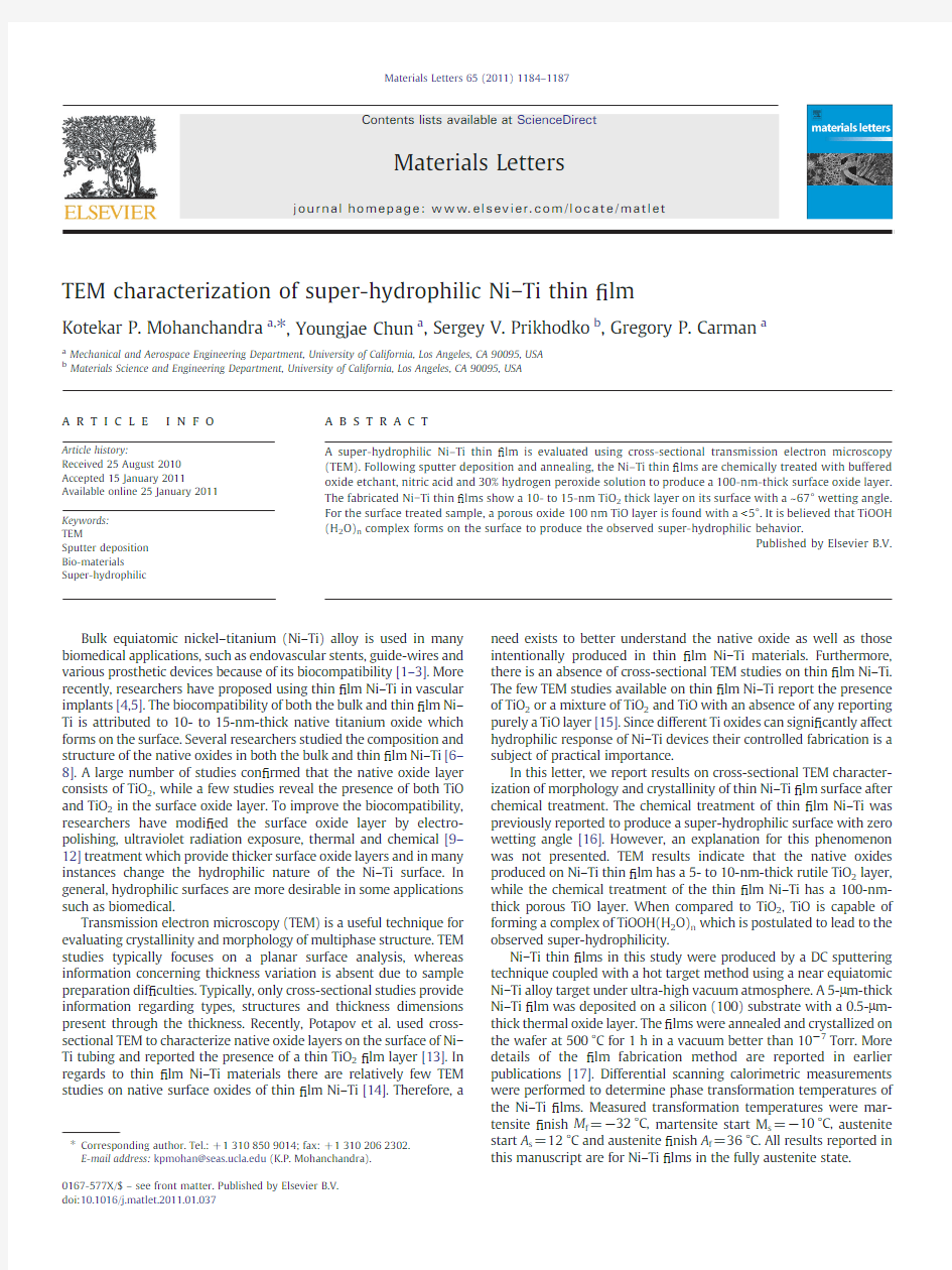
Following sputter deposition and annealing,the Ni –Ti thin ?lms were chemically treated as follows.First,the samples were immersed in buffered oxide etchant (BOE:aqueous NH 4-HF etchant)for 10min to remove the native oxide layer on the ?lm surface.The ?lms were subsequently treated by nitric acid (HNO 3)for 40min to remove excess nickel.Finally,the ?lms were immersed in 30%hydrogen peroxide (H 2O 2)solution for 14h.During the H 2O 2process it was observed that gas evolved and the ?lm surface color changed slowly to a slight yellowish tinge.This chemical treatment process produces a super-hydrophilic surface as described by Chun et al .[16].In this study,hydrophilicity of the samples was determined by measuring the wetting angles produced by water droplet on the ?lm surface.Fig.1shows the wetting angle measurements in either annealed or chemically treated Ni –Ti thin ?lms.The wetting angle for the annealed sample is 67°while for the chemically treated sample it is less than 5°.It has been previously reported that increases in hydrophilicity due to various surface treatments in Ni –Ti are attributed to the attachment of hydroxyl group (―OH)to the surface oxide layer [18].However,little information is available concerning the structure of the surface oxide layer and thus understanding the surface oxide characteristic is a critical concern.
Cross-sectional TEM samples are prepared from four different Ni –Ti thin ?lms:1)as annealed Ni –Ti thin ?lm (sample UT),2)after BOE (sample T1),3)after HNO 3(sample T2)and,4)after H 2O 2(sample T3)treatments.Samples were prepared by “lift-out ”method [13,19]using Nova 600dual-beam system (FEI).To protect the samples surface layers from the high energy focused Ga ion beam,a 0.1-μm-thick Pt was deposited on the Ni –Ti thin ?lm by electron beam deposition followed by a 0.9-μm-thick Pt deposited using ion beam.Ion milling produces a thin cross-sectional sample of size 10μm (length)×2μm (width)×7μm (depth)consisting of Ni –Ti/Oxide/Pt.After ?nal milling,the sample is lifted out with a needle-like probe and is subsequently attached to a TEM grid.The sample on the TEM grid is further thinned down from 2μm width to electron transpar-ency,less than 70nm,using a low ion beam current of 30pA.The entire sample preparation procedure was monitored using the secondary electron imaging mode inside Nova 600.Prepared samples were examined using scanning/transmission electron microscope(S/TEM)Titan (FEI)operating at accelerating voltage 300keV coupled with energy dispersive spectrometer (EDS)used for the elemental analysis.
The TEM micrographs of the four samples i.e.,annealed (UT)and three chemically treated Ni –Ti thin ?lms (T1,T2and T3),are shown in Fig.2a –d.The Pt surface protection layer is present in all the four
samples and visible on the right side of each image.Selective area electron diffraction (SAED)of the Si substrate was used to orient each sample in the TEM uniformly with the sample surface perpendicular to [100]zone axis.Fig.2a –c is procured at the same magni ?cation while Fig.2d is at a slightly lower magni ?cation.
Fig.2a shows the high resolution TEM (HRTEM)image of the surface oxide region of the UT sample.Beneath the Pt layer a 10-to 15-nm-thick polycrystalline native oxide layer is observed.The inset in Fig.2a shows the SAED ring pattern obtained from a 50nm diameter circular region containing the native oxide region,the Ni –Ti region,and the Pt coating.The indexed SAED pattern identi ?ed the oxide layer as rutile TiO 2#1-1292(JCPDS),tetragonal P42/mnm with a =4.58A,b =4.58and C =2.95A.The SAED ring pattern shows fundamental re ?ections from the {101},{111},{200},{211}and {002}planes in the TiO 2.The SAED pattern also shows fundamental re ?ections {200}and {220}of Pt and the {100}of parent Ni –Ti.SAED obtained from the parent Ni –Ti grain (not shown here)reveals a B2type structure.The parent Ni –Ti phase observed in all four sample studied (Fig.2a –d)in this paper is identical and is not discussed further.
Fig.2b –d represents TEM images of the samples taken after each of the three steps in the surface treatment to produce a super-hydrophilic layer.Fig.2b shows sample T1(following BOE etch to remove the 10-to 15-nm TiO 2)has a 10-nm-thick region directly adjacent to the Pt layer.This region was void of any spots or rings in the SAED indicating an amorphous structure.Based on STEM/EDS results the region closest to the Pt in Fig.2b contains relatively larger amount of Ni compared to the parent phase i.e.the Ni to Ti ratio (at %)changes from 1.22at the top surface (just below Pt)to 1.09at approximately 80nm from the top surface.We attribute this to the native oxide that formed following removal of the TiO 2layer reducing the Ti content.Fig.2c shows a TEM micrograph of sample T2(following HNO 3etch to remove Ni)with three distinct thin layers next to the Pt region.Since the sample T2was exposed to atmosphere following etching,a 2-nm-thick oxide layer forms on the sample.Beneath the oxide layer,one can observe two additional thin layers identi ?ed by different contrast.The lighter contrast indicates Ti rich region while the darker contrast indicates Ni rich region.Fig.2d shows sample T3(following H 2O 2to grow an oxide layer)has a 100-nm-thick layer next to the Pt region.This region is substantially larger than the surface regions observed in any of the previous TEM micrographs (Fig.2a –c).
A closer examination of the region in Fig.2d reveals the presence of TiO as explained below.Fig.3a is a SEM micrograph of the sample T3showing a 100-nm-thick porous layer beneath the Pt layers.Chu et al .[20]attributed submicron pores in bulk Ni –Ti alloy to chemical polish prior to H 2O 2treatment.In contrast,our study shows the submicron pores in the oxide layer formed after H 2O 2treatment on the Ni –Ti thin ?lm i.e.,not due to chemical polishing.HRTEM image of the surface oxide for sample T3is shown in Fig.3b.The image shows ?ne grains with sizes varying from 2to 5nm.The d-spacing is measured using a Digital-Micrograph software in conjunction with Fast Fourier Transform (FFT)dot patterns acquired at the individual grains along with the FFT ring pattern (inset of Fig.3b)acquired in a 20nm×20nm area.The d-spacing values measured corresponds to JCPDS data (#2-1196)for cubic TiO (space group:Fm3m,a =0.4235nm)as shown in Table 1.In addition,the SAED ring pattern shown in the inset of Fig.3b of this region also shows several diffraction rings.These diffraction rings also correspond to fundamental re ?ections from {200},{220},{222}and {311}of cubic TiO.
The TEM results show that the chemically treated Ni –Ti thin ?lms have a cubic TiO layer on its surface whereas the as annealed Ni –Ti thin ?lms have rutile TiO 2layer.The 0.3026nm spacing between the Ti atoms in the cubic TiO is nearly equal to the lattice spacing of Ni –Ti in the B2phase i.e.,0.3010nm.In contrast the 0.546nm spacing between nearest Ti atoms in rutile TiO 2is much larger than the lattice parameter of the B2phase.Therefore,we believe that the growth of cubic TiO
(100)
Fig. 1.Wetting angle measurements (a)before treatment,θ~67°,and (b)after treatment,θb 5.
1185
K.P.Mohanchandra et al./Materials Letters 65(2011)1184–1187
lattice parallel to the (100)lattice of B2is energetically more favorable at low temperature due to lattice matching [13].While this is postulated,we were unable to con ?rm epitaxial growth of TiO on Ni –Ti using HRTEM even though we were able to con ?rm the presence of TiO.In our study we used H 2O 2as an oxidizing agent to form a TiO layer on the Ni –Ti thin ?lms.The oxidization reaction proceeds by decomposition of H 2O 2into water and oxygen in the presence of Ti on the Ni –Ti thin ?lm surface.The gas that was observed during
the
Fig.2.TEM micrographs of (a)UT,(b)T1,(c)T2,and (d)T3
samples.
Fig.3.(a)SEM micrograph of sample T3.(b)HRTEM micrograph at the porous region.
1186K.P.Mohanchandra et al./Materials Letters 65(2011)1184–1187
immersion of Ni–Ti thin?lm into the H2O2solution suggests the oxygen production.The oxygen reacting with Ti produces TiO as con?rmed with TEM results.It is well established that H2O2reacts with Ti and also forms hydroxyl radicals(OH.).Highly reactive and short lived hydroxyl radicals further decompose the H2O2and produce more oxygen and water.This in turn produces a yellow colored TiOOH(H2O)n(i.e.as observed)complex as an end product and has been suggested previously for H2O2interaction with H2O2 [21].We believe that the yellow colored surface is a TiOOH(H2O)n complex on the Ni–Ti thin?lm surface and that this complex produces a surface exhibiting super-hydrophilic behavior.
Acknowledgment
This work is supported by the National Institutes of Health under award number1RC1HL099445-01.The authors have no con?icts of interest to disclose.References
[1]Stoeckel D.Min Invas Ther Allied Technol2000;9:81–8.
[2]Gil FJ,Planell JA.Proceedings of the Institution of Mechanical Engineers,Part H.J
Eng Med1998;212:473–88.
[3]Danilov A,Tuukkanen T,Tuukkanen J,J?ms?T.J Biomed Mater Res A2007;82:
810–919.
[4]Barras CDJ,Myers KA.Eur J Vasc Endovasc Surg2000;19:564–9.
[5]Shabalovskaya SA.Biomed Mater Eng2002;12:60–109.
[6]Michiardi A,Aparicio C,Planell JA,Gil FJ.J Biomed Mater Res Part B2006;77B:
249–56.
[7]Miyauchi M,Kieda N,Hishita S,Mitsuhashi T,Nakajima A,Watanabe T,et al.Surf
Sci2002;511:401–7.
[8]Maitz FM,Pham M,Wieser E,Tsyganov I.J Biomater Appl2003;17:303–18.
[9]Wu W,Liu X,Han H,Yang D,Lu S.J Mater Sci Technol2008;24:926–30.
[10]Chu CL,Want R,Yin L,Pu P,Dong YS,Guo C,et al.Trans Nonferrous Met Soc China
2009;19:575–80.
[11]Chu CL,Hu T,Wu SL,Dong YS,Yin LH,Yin YP,et al.Acta Biomater2007;3:795–806.
[12]Sun F,Sask KN,Brash JL,Zhitomirsky I.Colloids Surf,B2008;67:132--9.
[13]Potaov PL,Tirry W,Schryvers D,Sivel VGM,Wu Meng-Yue,Aslanidis D,et al.
J Mater Sci Mater Med2007;18:483–92.
[14]Wang X,Lai A,Vlassak JJ,Bellouard Y.Mater Res Soc Symp Proc2004;795PP
U8.201.1-6.
[15]Li YH,Li LM,Meng FL,Zheng WT,Zhao J,Wang YM.J Electron Spectrosc Relat
Phenom2006;15:144–8.
[16]Chun Y,Levi DS,Mohanchandra KP,Carman GP.Mater Sci Eng,C2009;29:
2436–42.
[17]Mohanchandra KP,Ho KK,Carman GP.Mater Lett2008;62:3481–3.
[18]Karuppuchamy S,Jeong JM.Materials science communication.Mater Chem Phys
2005;93:251–4.
[19]Tian H,Schryvers D,Shabalovskaya S,Van Humbeeck J.Microsc Microanal
2009;15:62–70.
[20]Chu CL,Chung CY,Chu PK.Mater Sci Eng,A2006;417:104–9.
[21]Tengvall P,Lundstrom I,Sjoqvist L,Elwing H.Biomaterials1989;10:166–75.
Table1
d-spacing and(h k l)indices from both FFT and SAED patterns.
d-spacing,nm (FFT)d-spacing,nm
(JCPDS:#2-1196)
(h k l)
from FFT
(dot pattern)
(h k l)
from FFT
ring pattern
(h k l)
from SAED
pattern
0.245±0.0030.245(111)
0.212±0.0020.212(200)(200)(200) 0.150±0.0040.150(220)(220)(220) 0.128±0.0020.128(311)(311) 0.122±0.0030.122(222)(222)1187
K.P.Mohanchandra et al./Materials Letters65(2011)1184–1187