________________General Description
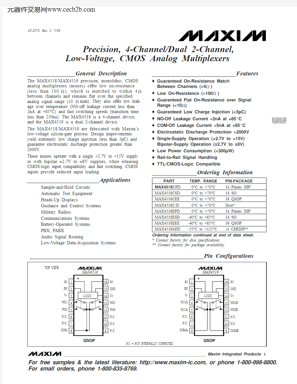
The MAX4518/MAX4519 precision, monolithic, CMOS analog multiplexers (muxes) offer low on-resistance (less than 100?), which is matched to within 4?between channels and remains flat over the specified analog signal range (10?max). They also offer low leak-age over temperature (NO-off leakage current less than 2nA at +85°C) and fast switching speeds (transition time less than 250ns). The MAX4518 is a 4-channel device,and the MAX4519 is a dual 2-channel device.
The MAX4518/MAX4519are fabricated with Maxim’s low-voltage silicon-gate process. Design improvements yield extremely low charge injection (less than 5pC) and guarantee electrostatic discharge protection greater than 2000V.
These muxes operate with a single +2.7V to +15V supply or with bipolar ±2.7V to ±8V supplies, while retaining CMOS-logic input compatibility and fast switching. CMOS inputs provide reduced input loading.
________________________Applications
Sample-and-Hold Circuits Automatic Test Equipment Heads-Up Displays
Guidance and Control Systems Military Radios
Communications Systems Battery-Operated Systems PBX, PABX
Audio Signal Routing
Low-Voltage Data-Acquisition Systems
____________________________Features
o Guaranteed On-Resistance Match Between Channels (<4?)o Low On-Resistance (<100?)
o Guaranteed Flat On-Resistance over Signal Range (<10?)
o Guaranteed Low Charge Injection (<5pC)o NO-Off Leakage Current <2nA at +85°C o COM-Off Leakage Current <5nA at +85°C o Electrostatic Discharge Protection >2000V o Single-Supply Operation (+2.7V to +15V)Bipolar-Supply Operation (±2.7V to ±8V)o Low Power Consumption (<300μW)o Rail-to-Rail Signal Handling o TTL/CMOS-Logic Compatible
_______________Ordering Information
* Contact factory for dice specifications.** Contact factory for package availability.
MAX4518/MAX4519
Precision, 4-Channel/Dual 2-Channel,Low-Voltage, CMOS Analog Multiplexers
________________________________________________________________Maxim Integrated Products
1
__________________________________________________________Pin Configurations
19-1070; Rev. 1; 5/98
For free samples & the latest literature: https://www.doczj.com/doc/055371902.html,, or phone 1-800-998-8800.For small orders, phone 1-800-835-8769.
M A X 4518/M A X 4519
Precision, 4-Channel/Dual 2-Channel,Low-Voltage, CMOS Analog Multiplexers 2_______________________________________________________________________________________
ABSOLUTE MAXIMUM RATINGS
ELECTRICAL CHARACTERISTICS—Dual Supplies
(V+ = +4.5V to +5.5V, V- = -4.5V to -5.5V, GND = 0V, V AH = V ENH = 2.4V, V AL = V ENL = 0.8V, T A = T MIN to T MAX , unless otherwise noted.)
Stresses beyond those listed under “Absolute Maximum Ratings” may cause permanent damage to the device. These are stress ratings only, and functional operation of the device at these or any other conditions beyond those indicated in the operational sections of the specifications is not implied. Exposure to absolute maximum rating conditions for extended periods may affect device reliability.
(Voltage Referenced to GND)
V+...........................................................................-0.3V to +17V V-............................................................................+0.3V to -17V V+ to V-...................................................................-0.3V to +17V Voltage into NO_, NC_ (Note 1).......(V- - 0.3V) to (V+ + 0.3V) or
30mA (whichever occurs first)
Voltage into EN, A0, A1 (Note 1)............(V- - 0.3V) to (V- + 17V)Current into Any Terminal...................................................30mA Peak Current, Any Terminal
(pulsed at 1ms, 10% duty cycle max)............................40mA
Continuous Power Dissipation (T A = +70°C)
Plastic DIP (derate 10.0mW/°C above +70°C)............800mW Narrow SO (derate 8.0mW/°C above +70°C)..............640mW QSOP (derate 9.52mW/°C above +70°C)....................762mW CERDIP (derate 9.09mW/°C above +70°C).................727mW Operating Temperature Ranges
MAX4518C_ _ /MAX4519C_ _............................0°C to +70°C MAX4518E_ _ /MAX4519E_ _..........................-40°C to +85°C MAX4518MJD/MAX4519MJD........................-55°C to +125°C Storage Temperature Range.............................-65°C to +150°C Lead Temperature (soldering, 10sec).............................+300°C
Note 1:Signals on any terminal exceeding V+ or V- are clamped by internal diodes. Limit forward current to maximum current ratings.
MAX4518/MAX4519
Precision, 4-Channel/Dual 2-Channel,Low-Voltage, CMOS Analog Multiplexers
_______________________________________________________________________________________3
ELECTRICAL CHARACTERISTICS—Dual Supplies (continued)
(V+ = +4.5V to +5.5V, V- = -4.5V to -5.5V, GND = 0V, V AH = V ENH = 2.4V, V AL = V ENL = 0.8V, T A = T MIN to T MAX , unless otherwise noted.)
M A X 4518/M A X 4519
Precision, 4-Channel/Dual 2-Channel,Low-Voltage, CMOS Analog Multiplexers 4_______________________________________________________________________________________
ELECTRICAL CHARACTERISTICS—Single +5V Supply
(V+ = +4.5V to +5.5V, V- = 0V, GND = 0V, V AH = V ENH = 2.4V, V AL = V ENL = 0.8V, T A = T MIN to T MAX , unless otherwise noted.)
MAX4518/MAX4519 Precision, 4-Channel/Dual 2-Channel, Low-Voltage, CMOS Analog Multiplexers
_______________________________________________________________________________________5
Note 2:The algebraic convention, where the most negative value is a minimum and the most positive value a maximum, is used in this data sheet.
Note 3:Guaranteed by design.
Note 4:?R ON= R ON(max) - R ON(min).
Note 5:Flatness is defined as the difference between the maximum and minimum value of on-resistance as measured over the specified analog signal ranges; i.e., V NO= 3V to 0V and 0V to -3V.
Note 6:Leakage parameters are 100% tested at maximum rated hot operating temperature, and guaranteed by correlation at +25°C.
Note 7:Worst-case isolation is on channel 4 because of its proximity to the COM pin. Off isolation = 20log V COM/V NO, V COM= output, V NO= input to off switch.
Note 8:Leakage testing at single supply is guaranteed by correlation testing with dual supplies.
ELECTRICAL CHARACTERISTICS—Single +5V Supply (continued)
(V+ = +4.5V to +5.5V, V- = 0V, GND = 0V, V AH= V ENH= 2.4V, V AL= V ENL= 0.8V, T A= T MIN to T MAX, unless otherwise noted.)
ELECTRICAL CHARACTERISTICS—Single +3V Supply
(V+ = +2.7V to +3.3V, V- = 0V, GND = 0V, V AH= V ENH= 2.4V, V AL= V ENL= 0.8V, T A= T MIN to T MAX, unless otherwise noted.)
M A X 4518/M A X 4519
Precision, 4-Channel/Dual 2-Channel,Low-Voltage, CMOS Analog Multiplexers 6_______________________________________________________________________________________
__________________________________________Typical Operating Characteristics
(T A = +25°C, unless otherwise noted.)
11030
-5-31
ON-RESISTANCE vs. V COM
(DUAL SUPPLIES)
5090
V COM (V)
R O N (?)
-1
3
701004080
605
-40
-22
4
11030
-5-31
ON-RESISTANCE vs. V COM
AND TEMPERATURE (DUAL SUPPLIES)
5090
V COM (V)
R O N (?)
-13
701004080
605
-40
-22
4
300
50
2
ON-RESISTANCE vs. V COM
(SINGLE SUPPLY)
100
200V COM (V)
R O N (?)
4
150250275225
751751251
5
3
1800
2
ON-RESISTANCE vs. V
COM AND TEMPERATURE (SINGLE SUPPLY)
100V COM (V)
R O N (?)
4
601401601208040
1
5
3
-5-31
CHARGE INJECTION vs. V
COM
-5
54321-1-2-3-4V COM (V)
Q j (p C )
-1
3
05
-40
-22
4
0.1
OFF-LEAKAGE vs.TEMPERATURE
1000
TEMPERATURE (°C)
O F F -L E A K A G E (p A )
10
1
100-50
125
25-25
07550
100
0.1
ON-LEAKAGE vs.TEMPERATURE
100010,000TEMPERATURE (°C)
O N -L E A K A G E (p A )
101
100
-50
125
25-25
07550100
0.1
SUPPLY CURRENT vs.
TEMPERATURE
10TEMPERATURE (°C)
I +, I - (n A )
1
-50
125
25-25
07550100
1
3
V+ SUPPLY CURRENT vs. LOGIC INPUT VOLTAGE
0.00001
100
LOGIC INPUT VOLTAGE (V)
V + S U P P L Y C U R R E N T (μA )
2
4
110
0.10.010.0010.0001
5
MAX4518/MAX4519
Precision, 4-Channel/Dual 2-Channel,Low-Voltage, CMOS Analog Multiplexers
_______________________________________________________________________________________7
______________________________________________________________Pin Description
M A X 4518/M A X 4519
__________Applications Information
Operation with Supply Voltages
Other than ±5V
Using supply voltages less than ±5V reduces the analog signal range. The MAX4518/MAX4519 muxes operate with ±2.7V to ±8V bipolar supplies or with a +2.7V to +15V single supply. Connect V- to GND when operating with a single supply. Both device types can also operate with unbalanced supplies, such as +10V and -5V. The Typical Operating Characteristics graphs show typical on-resistance with ±3V, ±5V, +3V and +5V supplies.(Switching times increase by a factor of two or more for operation at 5V.)
Overvoltage Protection
Proper power-supply sequencing is recommended for all CMOS devices. Do not exceed the absolute maxi-mum ratings, because stresses beyond the listed rat-ings can cause permanent damage to the devices.Always sequence V+ on first, then V-, followed by the logic inputs, NO, or COM. If power-supply sequencing is not possible, add two small signal diodes (D1, D2) in series with supply pins for overvoltage protection (Figure 1). Adding diodes reduces the analog signal range to one diode drop below V+ and one diode drop
above V-, but does not affect the devices’ low switch resistance and low leakage characteristics. Device operation is unchanged, and the difference between V+ and V- should not exceed 17V. These protection diodes are not recommended when using a single supply.
Precision, 4-Channel/Dual 2-Channel,Low-Voltage, CMOS Analog Multiplexers 8
_______________________________________________________________________________________
______________________________________________Test Circuits/Timing Diagrams
Figure 1. Overvoltage Protection Using External Blocking Diodes
Figure 2. Transition Time
MAX4518/MAX4519
Precision, 4-Channel/Dual 2-Channel,Low-Voltage, CMOS Analog Multiplexers
_______________________________________________________________________________________9
Figure 3. Enable Switching Time
_________________________________Test Circuits/Timing Diagrams (continued)
Figure 4. Break-Before-Make Interval
M A X 4518/M A X 4519
Precision, 4-Channel/Dual 2-Channel,Low-Voltage, CMOS Analog Multiplexers 10
______________________________________________________________________________________
Figure 5. Charge Injection
_________________________________Test Circuits/Timing Diagrams (continued)
Figure 6. Off Isolation, On Loss, Crosstalk
Figure 7. NO/COM Capacitance
MAX4518/MAX4519
Precision, 4-Channel/Dual 2-Channel,Low-Voltage, CMOS Analog Multiplexers
______________________________________________________________________________________
11
__________________________________________Functional Diagrams/Truth Tables
_____________________________________________Pin Configurations (continued)
M A X 4518/M A X 4519
Precision, 4-Channel/Dual 2-Channel,Low-Voltage, CMOS Analog Multiplexers Maxim cannot assume responsibility for use of any circuitry other than circuitry entirely embodied in a Maxim product. No circuit patent licenses are implied. Maxim reserves the right to change the circuitry and specifications without notice at any time.
12____________________Maxim Integrated Products, 120 San Gabriel Drive, Sunnyvale, CA 94086 408-737-7600?1998 Maxim Integrated Products
Printed USA
is a registered trademark of Maxim Integrated Products.
_Ordering Information (continued)
* Contact factory for dice specifications.** Contact factory for package availability.
__________________________________________________________Chip Topographies
NO4
NO3V+
NO1NO2
0.063"(1.6mm)
0.081"(2.05mm)
COM N.C.
V-EN
A0
A1GND
MAX4518
NO2B
NO1B V+
NO1A NO2A
0.063"(1.6mm)0.081"(2.05mm)
COMA COMB
MAX4519
SUBSTRATE CONNECTED TO V+
TRANSISTOR COUNT: 86SUBSTRATE CONNECTED TO V+