General Description
The MAX4460/MAX4461/MAX4462 are instrumentation amplifiers with precision specifications, low-power con-sumption, and excellent gain-bandwidth product.Proprietary design techniques allow ground-sensing capability combined with ultra-low input current and increased common-mode rejection performance. These Rail-to-Rail ?output instrumentation amplifiers are offered in fixed or adjustable gains and the option for either a shutdown mode or a pin to set the output voltage relative to an external reference (see Ordering Information and Selector Guide ).
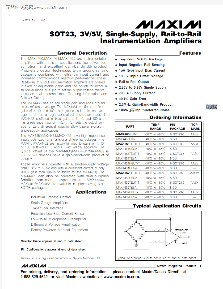
The MAX4460 has an adjustable gain and uses ground as its reference voltage. The MAX4461 is offered in fixed gains of 1, 10, and 100, uses ground as its reference volt-age, and has a logic-controlled shutdown input. The MAX4462 is offered in fixed gains of 1, 10, and 100 and has a reference input pin (REF). REF sets the output volt-age for zero differential input to allow bipolar signals in single-supply applications.
The MAX4460/MAX4461/MAX4462 have high-impedance inputs optimized for small-signal differential voltages. The MAX4461/MAX4462 are factory trimmed to gains of 1, 10,or 100 (suffixed U, T, and H) with ±0.1% accuracy. The typical offset of the MAX4460/MAX4461/MAX4462 is 100μV. All devices have a gain-bandwidth product of 2.5MHz.
These amplifiers operate with a single-supply voltage from 2.85V to 5.25V and with a quiescent current of only 700μA (less than 1μA in shutdown for the MAX4461). The MAX4462 can also be operated with dual supplies.Smaller than most competitors, the MAX4460/MAX4461/MAX4462 are available in space-saving 6-pin SOT23 packages.
________________________Applications
Industrial Process Control Strain-Gauge Amplifiers Transducer Interface
Precision Low-Side Current Sense Low-Noise Microphone Preamplifier Differential Voltage Amplification Battery-Powered Medical Equipment
Features
o Tiny 6-Pin SOT23 Package o Input Negative Rail Sensing o 1pA (typ) Input Bias Current o 100μV Input Offset Voltage o Rail-to-Rail Output
o 2.85V to 5.25V Single Supply o 700μA Supply Current o ±0.1% Gain Error
o 2.5MHz Gain-Bandwidth Product o 18nV/√Hz Input-Referred Noise
MAX4460/MAX4461/MAX4462
SOT23, 3V/5V , Single-Supply, Rail-to-Rail
Instrumentation Amplifiers
________________________________________________________________Maxim Integrated Products
1
19-2279; Rev 2; 11/02
For pricing, delivery, and ordering information,please contact Maxim/Dallas Direct!at 1-888-629-4642, or visit Maxim’s website at https://www.doczj.com/doc/0f5019785.html,.
Ordering Information
Rail-to-Rail is a registered trademark of Nippon Motorola, Ltd.
Pin Configurations appear at end of data sheet.
Typical Application Circuits
Selector Guide appears at end of data sheet.
M A X 4460/M A X 4461/M A X 4462
SOT23, 3V/5V , Single-Supply, Rail-to-Rail Instrumentation Amplifiers 2_______________________________________________________________________________________
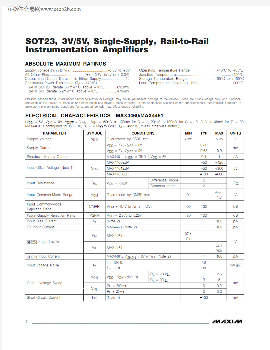
ABSOLUTE MAXIMUM RATINGS
Stresses beyond those listed under “Absolute Maximum Ratings” may cause permanent damage to the device. These are stress ratings only, and functional operation of the device at these or any other conditions beyond those indicated in the operational sections of the specifications is not implied. Exposure to absolute maximum rating conditions for extended periods may affect device reliability.
Supply Voltage (V DD to V SS ) ...................................-0.3V to +6V All Other Pins...................................(V SS - 0.3V) to (V DD + 0.3V)Output Short-Circuit Duration to Either Supply.........................1s Continuous Power Dissipation (T A = +70°C)
6-Pin SOT23 (derate 8.7mW/°C above +70°C)............695mW 8-Pin SO (derate 5.9mW/°C above +70°C)..................470mW
Operating Temperature Range ...........................-40°C to +85°C Junction Temperature......................................................+150°C Storage Temperature Range.............................-65°C to +150°C Lead Temperature (soldering, 10s)....................................300°C
ELECTRICAL CHARACTERISTICS—MAX4460/MAX4461
(V DD = 5V, V CM = 0V, V DIFF = V IN+- V IN-= 50mV to 100mV for G = 1, 20mV to 100mV for G = 10, 2mV to 48mV for G =100,MAX4460 is configured for G = 10, R L = 200k ?to GND, T A = +25°C , unless otherwise noted.)
MAX4460/MAX4461/MAX4462
SOT23, 3V/5V , Single-Supply, Rail-to-Rail
Instrumentation Amplifiers
ELECTRICAL CHARACTERISTICS —MAX4460/MAX4461 (continued)
ELECTRICAL CHARACTERISTICS —MAX4460/MAX4461
M A X 4460/M A X 4461/M A X 4462
SOT23, 3V/5V , Single-Supply, Rail-to-Rail Instrumentation Amplifiers 4_______________________________________________________________________________________
ELECTRICAL CHARACTERISTICS —MAX4460/MAX4461 (continued)
(V DD = 5V, V CM = 0V, V DIFF = V IN+- V IN-= 50mV to 100mV for G = 1, 20mV to 100mV for G = 10, 2mV to 48mV for G = 100,MAX4460 is configured for G = 10, R L = 200k ?to GND, T A = T MIN to T MAX , unless otherwise noted.)
MAX4460/MAX4461/MAX4462
SOT23, 3V/5V , Single-Supply, Rail-to-Rail
Instrumentation Amplifiers
_______________________________________________________________________________________5
ELECTRICAL CHARACTERISTICS —MAX4462
(V DD = 5V, V SS = 0V, V CM = V REF = V DD /2, R L = 100k ?to V DD /2, T A = +25°C , unless otherwise noted. V DIFF = V IN+- V IN-= -100mV
M A X 4460/M A X 4461/M A X 4462
SOT23, 3V/5V , Single-Supply, Rail-to-Rail Instrumentation Amplifiers 6_______________________________________________________________________________________
ELECTRICAL CHARACTERISTICS —MAX4462 (continued)
ELECTRICAL CHARACTERISTICS —MAX4462
MAX4460/MAX4461/MAX4462
SOT23, 3V/5V , Single-Supply, Rail-to-Rail
Instrumentation Amplifiers
_______________________________________________________________________________________7
ELECTRICAL CHARACTERISTICS —MAX4462 (continued)
Specifications section).
Note 2:Guaranteed by design, not production tested.
Note 3:Output swing high is measured only on G = 100 devices. Devices with G = 1 and G = 10 have output swing high limited by
the range of V REF , V CM , and V DIFF (see Output Swing section).
Note 4:Short-circuit duration limited to 1s (see Absolute Maximum Ratings).
Note 5:SOT23 units are 100% production tested at +25°C. Limits over temperature are guaranteed by design.
M A X 4460/M A X 4461/M A X 4462
SOT23, 3V/5V , Single-Supply, Rail-to-Rail Instrumentation Amplifiers 8_______________________________________________________________________________________
Typical Operating Characteristics
(V DD = 5V, V SS = 0V, V IN + = V IN-= V REF = V DD /2, R L = 100k ?to V DD /2, T A = +25°C, unless otherwise noted. V DIFF = V IN+- V IN-= -100mV to +100mV for G = 1 and G = 10, -20mV to +20mV for G = 100.)
10,0001000
10010
10.1
100
1
10
1k
10k
100k
INPUT VOLTAGE NOISE vs. FREQUENCY
M A X 4460 t o c 07
FREQUENCY (Hz)
I N P U T V O L T A G E N O I S E (n V /H z )
PEAK-TO-PEAK NOISE (0.1Hz TO 10Hz)
1s/div
2μV/div
INPUT REFERRED G = 1, 10, OR 100
0.0100.005
0.015
0.0200.0250.0300.0350.0400.04510
100
1k 10k
100k
TOTAL HARMONIC DISTORTION PLUS NOISE vs. FREQUENCY
FREQUENCY (Hz)
T H D + N (%)0
42108612141618-300
-200
-150
-250
-100
-50
50
100
150
200
250
300
VOLTAGE OFFSET HISTOGRAM
VOLTAGE OFFSET (μV)
P E R C E N T A G E O F U N I T S
4261214108160
0.02
0.030.040.050.010.060.070.080.090.10
GAIN-LINEARITY HISTOGRAM
LINEARITY (%)P E R C E N T A G E O F U N I T S
426121410816-5-3-2-10
-412345
VOLTAGE OFFSET DRIFT HISTOGRAM
VOLTAGE OFFSET DRIFT (μV/°C)P E R C E N T A G E O F U N I T S
4
2861012-0.50GAIN ERROR HISTOGRAM
GAIN ERROR (%)
P E R C E N T A G E O F U N I T
S
-0.4-0.2-0.10.10.20.30.40.5
-0.3-130
-120-90-100-110-80-70-60-50-40-30-20
0.1
10
1
100
1k
10k
COMMON-MODE REJECTION RATIO
vs. FREQUENCY
FREQUENCY (Hz)C M R R (d B )
POWER-SUPPLY REJECTION RATIO
VS. FREQUENCY
FREQUENCY (Hz)
0.01101001k 0.1110k
P S R R (d B )
-120
-100-80
-60-20
-40
MAX4460/MAX4461/MAX4462
SOT23, 3V/5V , Single-Supply, Rail-to-Rail
Instrumentation Amplifiers
_______________________________________________________________________________________9
300
65040080075070090095085010002.75 3.503.753.003.25 4.004.254.504.755.00
SUPPLY CURRENT
VS. SUPPLY VOLTAGE
SUPPLY VOLTAGE (V)S U P P L Y C U R R E N T (μA )
6005505004503500
4286121014SHUTDOWN CURRENT VS. SUPPLY VOLTAGE
SUPPLY VOLTAGE (V)
S U P P L Y C U R R E N T (n A )
2.75
3.503.753.003.25
4.004.254.504.75
5.00
00.040.020.080.060.120.10
0.140.180.160.20
0.20.30.40.10.50.60.70.90.8 1.0
MAX4462H
NORMALIZED OUTPUT ERROR vs. COMMON-MODE VOLTAGE
V CM (V)
N O R M A L I Z E D O U T P U T E R R O R (%
)-0.30
-0.16-0.18-0.20-0.22-0.24-0.26-0.28-0.12-0.14-0.08-0.10-0.06-0.02-0.040-2.7-2.1-1.8-2.4-1.5-1.2-0.9-0.60
-0.3MAX4462H
NORMALIZED OUTPUT ERROR vs. COMMON-MODE VOLTAGE
V CM (V)
N O R M A L I Z E D O U T P U T E R R O R (%)
04020
80601201001401801602000
2
3
4
1
5
6
7
9
8
10
OUTPUT SWING HIGH
VS. OUTPUT CURRENT
OUTPUT CURRENT (mA)
V D D - V O U T (m V )
10050200150
300250350450400500
023*********
OUTPUT SWING LOW vs. OUTPUT CURRENT
OUTPUT CURRENT (mA)
V O U T - V S S (m V )
Typical Operating Characteristics (continued)
(V DD = 5V, V SS = 0V, V IN + = V IN-= V REF = V DD /2, R L = 100k ?to V DD /2, T A = +25
°C, unless otherwise noted. V DIFF = V IN+- V IN-= -100mV to +100mV for G = 1 and G = 10, -20mV to +20mV for G = 100.)
-10100
3020
4050GAIN vs. FREQUENCY
FREQUENCY (Hz)G A I N (d B
)
0.01
1
10
0.1
100
1k
10k 22
23
25
24
2627
-4010-15356085GAIN BANDWIDTH vs. TEMPERATURE
TEMPERATURE (°C)
-3d B B A N D W I D T H (k H z )
SETTLING TIME (GAIN = 100)
MAX4460 toc18
40μs/div
INPUT 10mV/div
OUTPUT 500mV/div
OUTPUT 10mV/div
M A X 4460/M A X 4461/M A X 4462
SOT23, 3V/5V , Single-Supply, Rail-to-Rail Instrumentation Amplifiers 10______________________________________________________________________________________
Typical Operating Characteristics (continued)
(V DD = 5V, V SS = 0V, V IN + = V IN-= V REF = V DD /2, R L = 100k ?to V DD /2, T A = +25°C, unless otherwise noted. V DIFF = V IN+- V IN-= -100mV to +100mV for G = 1 and G = 10, -20mV to +20mV for G = 100.)
LARGE-SIGNAL PULSE RESPONSE
(GAIN = 1V/V)
MAX4460 toc19
INPUT
OUTPUT
50mV/div
1μs/div LARGE-SIGNAL PULSE RESPONSE
(GAIN = 100V/V)
MAX4460 toc20
INPUT 10mV/div
OUTPUT 1V/div
20μs/div
SMALL-SIGNAL PULSE RESPONSE
(GAIN = 1V/V)
MAX4460 toc21
INPUT
OUTPUT
10mV/div
1μs/div
SMALL-SIGNAL PULSE RESPONSE
(GAIN = 1V/V)
1μs/div
INPUT 10mV/div
OUTPUT
C L = 100pF
SMALL-SIGNAL PULSE RESPONSE
(GAIN = 100V/V)
MAX4460 toc23
INPUT 1mV/div OUTPUT 100mV/div
20μs/div
SMALL-SIGNAL PULSE RESPONSE
(GAIN = 100V/V)
X 4460 t o c 24
20μs/div
INPUT 1mV/div
OUTPUT 100mV/div
GAIN = +100V/V C L = 100pF
C L = 100pF
MAX4460/MAX4461/MAX4462
SOT23, 3V/5V , Single-Supply, Rail-to-Rail
Instrumentation Amplifiers
______________________________________________________________________________________11
Pin Descriptions
M A X 4460/M A X 4461/M A X 4462
SOT23, 3V/5V , Single-Supply, Rail-to-Rail Instrumentation Amplifiers 12______________________________________________________________________________________
Detailed Description
The MAX4460/MAX4461/MAX4462 family of instrumen-tation amplifiers implements Maxim ’s proprietary indi-rect current-feedback design to achieve a precision specification and excellent gain-bandwidth product.These new techniques allow ground-sensing capability combined with an ultra-low input current and an increased common-mode rejection.
The differential input signal is converted to a current by an input transconductance stage. An output transcon-ductance stage converts a portion of the output voltage (equal to the output voltage divided by the gain) into another precision current. These two currents are sub-tracted and the result is fed to a loop amplifier with a class AB output stage with sufficient gain to minimize errors (Figure 1).
The MAX4461U/T/H and MAX4462U/T/H have factory-trimmed gains of 1, 10, and 100, respectively. The MAX4460 has an adjustable gain, set with an external pair of resistors between pins OUT, FB, and GND (Figure 2).
The MAX4462U/T/H has a reference input (REF) which is connected to an external reference for bipolar opera-tion of the device. The range for V REF is 0.1V to (V DD -1.7V). For full output-swing capability, optimal perfor-mance is usually obtained with V REF = V DD /2.
The MAX4460/MAX4461/MAX4462 operate with single-supply voltages of 2.85V to 5.25V. It is possible to use the MAX4462U/T/H in a dual-supply configuration with up to ±2.6V at V DD and V SS , with REF connected to ground.
The MAX4461U/T/H has a shutdown feature to reduce the supply current to less than 1μA. The MAX4461U/T/H output is internally referenced to ground, making the part suitable for unipolar operations.
The MAX4460 has an FB pin that can be used to exter-nally set the gain through a pair of resistors (see Setting the Gain (MAX4460) section). The MAX4460 output is internally referenced to ground, making the part suitable for unipolar operations.
Figure 1. Functional Diagrams
Figure 2. MAX4460 External Resistor Configuration
Functional Diagrams
MAX4460/MAX4461/MAX4462
SOT23, 3V/5V , Single-Supply, Rail-to-Rail
Instrumentation Amplifiers
______________________________________________________________________________________13
Input Common-Mode and Output
Reference Ranges
MAX4460/MAX4461/MAX4462 have an input common-mode range of 100mV below the negative supply to 1.7V below the positive supply.
The output reference voltage of MAX4462U/T/H is set by REF and ranges from 100mV above the negative supply to 1.7V below the positive supply. For maximum voltage swing in a bipolar operation, connect REF to V DD /2. The output voltages of the MAX4460 and MAX4461U/T/H are referenced to ground. Unlike the traditional three-op-amp configuration of common instrumentation amplifiers, the MAX4460/MAX4461/MAX4462 have ground-sensing capability (or to V SS in dual-supply configuration) in addition to the extremely high input impedances of MOS input differential pairs.
Input Differential Signal Range
The MAX4460/MAX4461/MAX4462 feature a proprietary input structure optimized for small differential signals.The unipolar output of the MAX4460/MAX4461 is nomi-nally zero-for-zero differential input. However, these devices are specified for inputs of 50mV to 100mV for the unity-gain devices, 20mV to 100mV for gain of 10devices, and 2mV to 48mV for gain of 100 devices. The MAX4460/MAX4461 can be used with differential inputs approaching zero, albeit with reduced accuracy.
The bipolar output of the MAX4462 allows bipolar input ranges. The output voltage is equal to the reference voltage for zero differential input. The MAX4462 is specified for inputs of ±100mV for the unity gain and gain of 10 devices, and ±20mV for gain of 100 devices.The gain of 100 devices (MAX4462H) can be operated beyond 20mV signal provided the reference is chosen for unsymmetrical swing.
Output Swing
The MAX4460/MAX4461/MAX4462 are designed to have rail-to-rail output voltage swings. However,depending on the selected gain and supply voltage (and output reference level of the MAX4462), the rail-to-rail output swing is not required.
For example, consider the MAX4461U, a unity-gain device with its ground pin as the output reference level.The input voltage range is 0 to 100mV (50mV minimum to meet accuracy specifications). Because the device is unity gain and the output reference level is ground,the output only sees excursions from ground to 100mV.Devices with higher gain and with bipolar output such as the MAX4462, can be configured to swing to higher
levels. In these cases, as the output approaches either supply, accuracy may degrade, especially under heavy output loading.
Shutdown Mode
The MAX4461U/T/H features a low-power shutdown mode. When the SHDN pin is pulled low, the internal transconductance and amplifier blocks are switched off and supply current drops to typically less than 0.1μA (Figure 1).
I n shutdown, the amplifier output is high impedance.The output transistors are turned off, but the feedback resistor network remains connected. If the external load is referenced to GND, the output drops to approximate-ly GND in shutdown. The output impedance in shut-down is typically greater than 100k ?. Drive SHDN high or connect to V CC for normal operation.
A User Guide to Instrumentation Amplifier Accuracy Specifications
As with any other electronic component, a complete understanding of instrumentation amplifier specifica-tions is essential to successfully employ these devices in their application circuits. Most of the specifications for these differential closed-loop gain blocks are similar to the well-known specifications of operational ampli-fiers. However, there are a few accuracy specifications that could be confusing to first-time users. Therefore,some explanations and examples may be helpful.
Accuracy specifications are measurements of close-ness of an actual output response to its ideal expected value. There are three main specifications in this category:
G Gain error
G Gain nonlinearity error
G
Offset error
In order to understand these terms, we must look at the transfer function of an ideal instrumentation amplifier. As expected, this must be a straight line passing through origin with a slope equal to the ideal gain (Figure 3). I f the ideal gain is equal to 10 and the extreme applied input voltages are -100mV and +100mV, then the value of the output voltages are -1V and +1V, respectively.Note that the line passes through the origin and therefore a zero input voltage gives a zero output response.
The transfer function of a real instrumentation amplifier is quite different from the ideal line pictured in Figure 3.Rather, it is a curve such as the one indicated as the typical curve in Figure 4, connecting end points A and B.
M A X 4460/M A X 4461/M A X 4462
SOT23, 3V/5V , Single-Supply, Rail-to-Rail Instrumentation Amplifiers 14______________________________________________________________________________________
Looking at this curve, one can immediately identify three types of errors.
First, there is an obvious nonlinearity (curvature) when this transfer function is compared to a straight line.More deviation is measured as greater nonlinearity error. This is explained in more detail below.
Second, even if there was no nonlinearity error, i.e., the actual curve in Figure 4 was a straight line connecting end points A and B, there exists an obvious slope devi-ation from that of an ideal gain slope (drawn as the “ideal ” line in Figure 4). This rotational error (delta slope) is a measure of how different the actual gain (G A ) is from the expected ideal gain (G I)and is called gain error (GE) (see the equation below).
Third, even if the actual curve between points A and B was a straight line (no nonlinearity error) and had the same slope as the ideal gain line (no gain error), there is still another error called the end-point offset error (OE on vertical axis), since the line is not passing through the origin.
Figure 5 is the same as Figure 4, but the ideal line (CD)is shifted up to pass through point E (the Y intercept of end-points line AB).
This is done to better visualize the rotational error (GE),which is the difference between the slopes of end points line AB and the shifted ideal line CD. Mathematically:
GE (%) = 100 x (G A - G I ) / G I
Figure 5. Typical Transfer Function for a Real Instrumentation Amplifier (Ideal Line (CD) Is Shifted by the End-Points Offset (OE) to Visualize Gain Error)
MAX4460/MAX4461/MAX4462
SOT23, 3V/5V , Single-Supply, Rail-to-Rail
Instrumentation Amplifiers
______________________________________________________________________________________15
The rotational nature of gain error, and the fact that it is pivoted around point E in Figure 5, shows that gain-error contribution to the total output voltage error is directly proportional to the input voltage. At zero input voltage, the error contribution of gain error is zero, i.e.,the total deviation from the origin (the expected zero output value) is only due to end-points OE and nonlin-earity error at zero value of input (segment EZ on the vertical axis).
The nonlinearity is the maximum deviation from a straight line, and the end-point nonlinearity is the devia-tion from the end-point line. As shown in Figure 5, it is likely that two nonlinearities are encountered, one posi-tive and the other a negative nonlinearity error, shown as NL+ and NL- in Figure 5.
Generally, NL+ and NL- have different values and this remains the case if the device is calibrated (trimmed)for end-points errors (which means changing the gain of the instrumentation amplifier in such a way that the slope of line AB becomes equal to that of CD, and the offset becomes trimmed such that OE vanishes to zero). This is an undesirable situation when nonlinearity is of prime interest.
The straight line shown in Figure 6 is in parallel to end-points line AB and has a Y intercept of OS on the verti-cal axis. This line is a shifted end-points line such that the positive and negative nonlinearity errors with respect to this line are equal. For this reason, the line is called the best straight line (BSL). Maxim internally trims the MAX4460/MAX4461/MAX4462 with respect to this line (changing the gain slope to be as close as possible to the slope of the ideal line and trimming the offset such that OS gets as close to the origin as possi-ble) to minimize all the errors. The total accuracy error is still the summation of the gain error, nonlinearity, and offset errors.
As an example, assume the following specification for an instrumentation amplifier:
Gain = 10GE = 0.15%
Offset (BSL) = 250μV NL = 0.05%
V DIF (input) = -100mV to +100mV
What is the maximum total error associated with the GE, offset (BSL), and NL? With a differential input range of -0.1V to +0.1V and a gain of 10, the output voltage assumes a range of -1V to +1V, i.e., a total full-scale range of 2V.
The individual errors are as follows:
GE = (0.15%) (10) (100mV) = 1.5mV Offset (BSL) = (250μV) (10) = 2.5mV
NL = (0.05%) (2V) = 1mV
Maximum Total Error = 1.5mV + 2.5mV + 1mV
= 5mV
So, the absolute value of the output voltage, consider-ing the above errors, would be at worst case between 0.995V to 1.005V. Note that other important parameters such as PSRR, CMRR, and noise also contribute to the total error in instrumentation applications. They are not considered here.
Figure 6. To Minimize Nonlinearity Error, the MAX4460/MAX4461/MAX4462 are Internally Trimmed to Adjust Gain and Offset for the Best Straight Line so NL- = NL+
M A X 4460/M A X 4461/M A X 4462
SOT23, 3V/5V , Single-Supply, Rail-to-Rail Instrumentation Amplifiers 16______________________________________________________________________________________
Applications Information
Setting the Gain (MAX4460)
The MAX4460 gain is set by connecting a resistive-divider from OUT to GND, with the center tap connect-ed to FB (Figure 2). The gain is calculated by:
Gain = 1 + R2 / R1
Because FB has less than 100pA IB, high-valued resis-tors can be used without significantly affecting the gain accuracy. The sum of resistors (R1 + R2) near 100k ?is a good compromise. Resistor accuracy directly affects gain accuracy. Resistor sum less than 20k ?should not be used because their loading can slightly affect output accuracy.
Capacitive-Load Stability
The MAX4460/MAX4461/MAX4462 are capable of dri-ving capacitive loads up to 100pF.
Applications needing higher capacitive drive capability may use an isolation resistor between OUT and the load to reduce ringing on the output signal. However this reduces the gain accuracy due to the voltage drop across the isolation resistor.
Output Loading
For best performance, the output loading should be to the potential seen at REF for the MAX4462 or to ground for the MAX4460/MAX4461.
REF Input (MAX4462)
The REF input of the MAX4462 can be connected to any voltage from (V SS + 0.1V) to (V DD - 1.7V). A buffered voltage-divider with sink and source capability works well to center the output swing at V DD /2. Unbuffered resistive dividers should be avoided because the 100k ?(typ) input impedance of REF causes amplitude-depen-dent variations in the divider ’s output.
Bandgap references, either series or shunt, can be used to drive REF. This provides a voltage and temper-ature invariant reference. This same reference voltage can be used to bias bridge sensors to eliminate supply voltage ratiometricity. For proper operation, the refer-ence must be able to sink and source at least 25μA.I n many applications, the MAX4462 is connected to a CODEC or other device with a reference voltage out-put. In this case, the receiving device ’s reference out-put makes an ideal reference voltage. Verify the reference output of the device is capable of driving the MAX4462’s REF input.
Power-Supply Bypass and Layout
Good layout technique optimizes performance by decreasing the amount of stray capacitance at the instrumentation amplifier ’s gain-setting pins. Excess capacitance produces peaking in the amplifier ’s fre-quency response. To decrease stray capacitance, min-imize trace lengths by placing external components as close to the instrumentation amplifier as possible. For best performance, bypass each power supply to ground with a separate 0.1μF capacitor.
Microphone Amplifier
The MAX4462’s bipolar output, along with its excellent common-mode rejection ratio, makes it suitable for pre-cision microphone amplifier applications. Figure 7 illus-trates one such circuit. I n this case, the electret microphone is resistively biased to the supply voltage through a 2.2k ?pullup resistor. The MAX4462 directly senses the output voltage at its noninverting input, and indirectly senses the microphone ’s ground through an AC-coupling capacitor. This technique provides excel-lent rejection of common-mode noise picked up by the microphone lead wires. Furthermore, ground noise from distantly located microphones is reduced.
The single-ended output of the MAX4462 is converted to differential through a single op amp, the MAX4335. The op amp forces the midpoint between OUT+ and OUT- to be equal to the reference voltage. The configuration does not change the MAX4662T ’s fixed gain of 10.
MAX4460/MAX4461/MAX4462
SOT23, 3V/5V , Single-Supply, Rail-to-Rail
Instrumentation Amplifiers
______________________________________________________________________________________17
Figure 7. Differential I/O Microphone Amplifier
Chip Information
TRANSISTOR COUNT: 421PROCESS: BiCMOS
Typical Application Circuits
(continued)
M A X 4460/M A X 4461/M A X 4462
SOT23, 3V/5V , Single-Supply, Rail-to-Rail Instrumentation Amplifiers 18______________________________________________________________________________________
Pin Configurations
MAX4460/MAX4461/MAX4462
SOT23, 3V/5V , Single-Supply, Rail-to-Rail
Instrumentation Amplifiers
______________________________________________________________________________________19
Package Information
(The package drawing(s) in this data sheet may not reflect the most current specifications. For the latest package outline information,go to https://www.doczj.com/doc/0f5019785.html,/packages .)
M A X 4460/M A X 4461/M A X 4462
SOT23, 3V/5V , Single-Supply, Rail-to-Rail Instrumentation Amplifiers Maxim cannot assume responsibility for use of any circuitry other than circuitry entirely embodied in a Maxim product. No circuit patent licenses are implied. Maxim reserves the right to change the circuitry and specifications without notice at any time.
20____________________Maxim Integrated Products, 120 San Gabriel Drive, Sunnyvale, CA 94086 408-737-7600?2002 Maxim Integrated Products
Printed USA
is a registered trademark of Maxim Integrated Products.
Package Information (continued)
(The package drawing(s) in this data sheet may not reflect the most current specifications. For the latest package outline information,go to https://www.doczj.com/doc/0f5019785.html,/packages .)