White Electronic Designs
WS1M8V-XCX
ADVANCED*
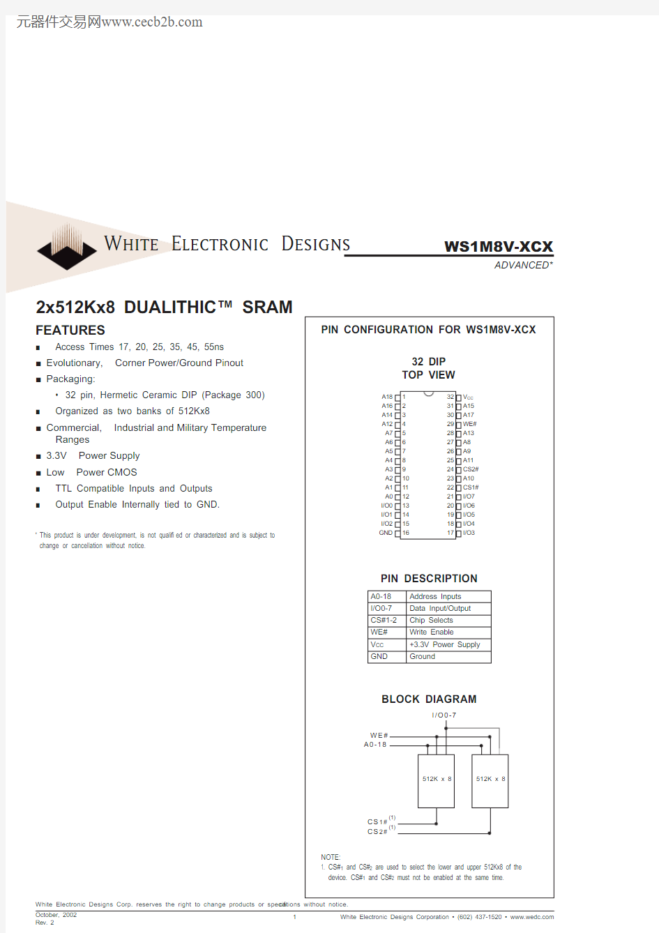
2x512Kx8 DUALITHIC? SRAM Array FEATURES
■ Access Times 17, 20, 25, 35, 45, 55ns
Pinout
Corner
■ Evolutionary,
Power/Ground
■ Packaging:
? 32 pin, Hermetic Ceramic DIP (Package 300)
■ Organized as two banks of 512Kx8
Temperature
Military
Industrial
■ Commercial,
and
Ranges
Supply
Power
■ 3.3V
CMOS
Power
■ Low
■ TTL Compatible Inputs and Outputs
■ Output Enable Internally tied to GND.
* T his product is under development, is not quali? ed or characterized and is subject to
change or cancellation without notice.
WS1M8V-XCX White Electronic Designs
ADVANCED*
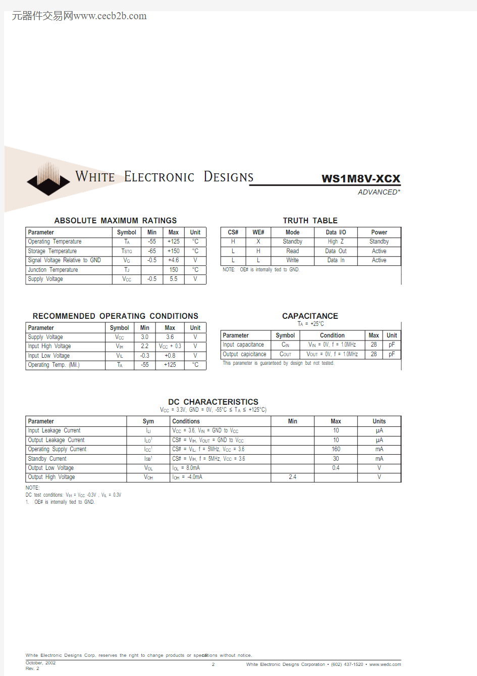
ABSOLUTE MAXIMUM RATINGS Parameter Symbol Min Max Unit Operating Temperature T A-55+125°C Storage Temperature T STG-65+150°C Signal Voltage Relative to GND V G-0.5+4.6V Junction Temperature T J150°C Supply Voltage V CC-0.5 5.5V
TRUTH TABLE
CS#WE#Mode Data I/O Power
H X Standby High Z Standby
L H Read Data Out Active
L L Write Data In Active NOTE: OE# is internally tied to GND.
CAPACITANCE
T A = +25°C
Parameter Symbol Condition Max Unit Input capacitance C IN V IN = 0V, f = 1.0MHz28pF Output capicitance C OUT V OUT = 0V, f = 1.0MHz28pF This parameter is guaranteed by design but not tested.
RECOMMENDED OPERATING CONDITIONS
Parameter Symbol Min Max Unit
Supply Voltage V CC 3.0 3.6V
Input High Voltage V IH 2.2V CC + 0.3V
Input Low Voltage V IL-0.3+0.8V
Operating Temp. (Mil.)T A-55+125°C
DC CHARACTERISTICS
V CC = 3.3V, GND = 0V, -55°C ≤ T A ≤ +125°C)
Parameter Sym Conditions Min Max Units Input Leakage Current I LI V CC = 3.6, V IN = GND to V CC10μA Output Leakage Current I LO1CS# = V IH, V OUT = GND to V CC10μA Operating Supply Current I CC1CS# = V IL, f = 5MHz, V CC = 3.6160mA Standby Current I SB1CS# = V IH, f = 5MHz, V CC = 3.630mA Output Low Voltage V OL I OL = 8.0mA0.4V Output High Voltage V OH I OH = -4.0mA 2.4V NOTE:
DC test conditions: V IH = V CC -0.3V , V IL = 0.3V
1. OE# is internally tied to GND.
White Electronic Designs
WS1M8V-XCX
ADVANCED*
AC CHARACTERISTICS
V CC = 3.3V, GND = 0V, -55°C ≤ T A ≤ +125°C)
Parameter Symbol-17-20-25-35-45-55Units Read Cycle Min Max Min Max Min Max Min Max Min Max Min Max
Read Cycle Time t RC172025354555ns Address Access Time t AA172025354555ns Output Hold from Address Change t OH000000ns Chip Select Access Time t ACS172025354555ns Chip Select to Output in Low Z t CLZ1222444ns Chip Disable to Output in High Z t CHZ191012152020ns NOTES:
1. This parameter is guaranteed by design but not tested.
2. OE# is internally tied to GND.
AC CHARACTERISTICS
V CC = 3.3V, GND = 0V, -55°C ≤ T A ≤ +125°C)
Parameter Symbol-17-20-25-35-45-55Units Write Cycle Min Max Min Max Min Max Min Max Min Max Min Max
Write Cycle Time t WC 172025354555ns Chip Select to End of Write t CW141415253550ns Address Valid to End of Write t AW141415253550ns Data Valid to End of Write t DW91010202525ns Write Pulse Width t WP141415253540ns Address Setup Time t AS000000ns Address Hold Time t AH000055ns Output Active from End of Write t OW1234455ns Write Enable to Output in High Z t WHZ199********ns Data Hold Time t DH000000ns NOTES:
1. This parameter is guaranteed by design but not tested.
White Electronic Designs
WS1M8V-XCX
ADVANCED* TIMING WAVEFORM – READ CYCLE
White Electronic Designs
WS1M8V-XCX
ADVANCED*
PACKAGE 300: 32 PIN, CERAMIC DIP, SINGLE CAVITY SIDE BRAZED