
UC2901
UC3901 Isolated Feedback Generator
FEATURES
?An Amplitude-Modulation System for Transformer Coupling an Isolated Feedback Error Signal
?Low-Cost Alternative to Optical Couplers
?Internal 1% Reference and Error Amplifier
?Internal Carrier Oscillator Usable to 5MHz
?Modulator Synchronizable to an External Clock
?Loop Status Monitor DESCRIPTION
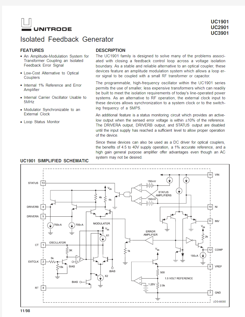
The UC1901family is designed to solve many of the problems associ-ated with closing a feedback control loop across a voltage isolation boundary.As a stable and reliable alternative to an optical coupler,these devices feature an amplitude modulation system which allows a loop er-ror signal to be coupled with a small RF transformer or capacitor.
The programmable,high-frequency oscillator within the UC1901series permits the use of smaller,less expensive transformers which can readily be built to meet the isolation requirements of today's line-operated power systems.As an alternative to RF operation,the external clock input to these devices allows synchronization to a system clock or to the switch-ing frequency of a SMPS.
An additional feature is a status monitoring circuit which provides an active-low output when the sensed error voltage is within±10%of the reference. The DRIVERA output,DRIVERB output,and STATUS output are disabled until the input supply has reached a sufficient level to allow proper operation of the device.
Since these devices can also be used as a DC driver for optical couplers, the benefits of4.5to40V supply operation,a1%accurate reference,and a high gain general purpose amplifier offer advantages even though an AC system may not be desired.
UC1901 SIMPLIFIED SCHEMATIC
ABSOLUTE MAXIMUM RATINGS (Note 1)
Input Supply Voltage, V IN . . . . . . . . . . . . . . . . . . . . . . . . . .40V Reference Output Current . . . . . . . . . . . . . . . . . . . . . . .–10mA Driver Output Currents . . . . . . . . . . . . . . . . . . . . . . . . . .–35mA Status Indicator Voltage . . . . . . . . . . . . . . . . . . . . . . . . . . .40V Status Indicator Current . . . . . . . . . . . . . . . . . . . . . . . . . .20mA Ext. Clock Input . . . . . . . . . . . . . . . . . . . . . . . . . . . . . . . . . .40V Error Amplifier Inputs . . . . . . . . . . . . . . . . . . . . .–0.5V to +35V Power Dissipation at T A = 25°C. . . . . . . . . . . . . . . . . .1000mW Power Dissipation at T C = 25°C . . . . . . . . . . . . . . . . .2000mW Operating Junction Temperature . . . . . . . . . .–55°C to +150°C Storage Temperature . . . . . . . . . . . . . . . . . . .–65°C to +150°C Lead Temperature (Soldering, 10 seconds). . . . . . . . . .300°C
Note 1:Voltages are referenced to ground,Pin 7.Currents are positive into, negative out of the specified terminal.
Note 2:Consult Packaging section of Databook for thermal limi-
tations and considerations of package.
CONNECTION DIAGRAMS
TEMPERATURE
RANGE AVAILABLE PACKAGES
UC1901–55°C to +125°C J, L
UC2901–40°C to +85°C D, DW, J, N, Q UC3901
0°C to +70°C
D, DW, J, N, Q
TEMPERATURE AND PACKAGE SELECTION GUIDE
ELECTRICAL CHARACTERISTICS Unless otherwise stated, these specifications apply for V IN= 10V, R T= 10k?, C T= 820pF, T A= T J.
PARAMETER TEST CONDITIONS UC1901/UC2901UC3901UNITS
MIN TYP MAX MIN TYP MAX Reference Section
Output Voltage T J= 25°C 1.485 1.5 1.515 1.47 1.5 1.53V
T MIN≤T J≤T MAX 1.470 1.5 1.530 1.455 1.5 1.545 Line Regulation V IN= 4.5 to 35V210215mV Load Regulation I OUT= 0 to 5mA410415mV Short Circuit Current T J= 25°C–35–55–35–55mV Error Amplifier Section(To Compensation Terminal)
Input Offset Voltage V CM= 1.5V1418mV Input Bias Current V CM= 1.5V–1–3–1–6μA Input Offset Current V CM= 1.5V0.110.12μA Small Signal Open Loop Gain40604060dB CMRR V CM= 0.5 to 7.5V60806080dB PSRR V IN= 2 to 25V8010080100dB Output Swing,?V O0.40.70.40.7V Maximum Sink Current9015090150μA Maximum Source Current–2–3–2–3mA Gain Band Width Product11MHz Slew Rate0.30.3V/μS Modulators/Drivers Section(From Compensation Terminal)
Voltage Gain111213101214dB Output Swing±1.6±2.8±1.6±2.8V Driver Sink Current500700500700μA Driver Source Current–15–35–15–35mA Gain Band Width Product2525MHz Oscillator Section
Initial Accuracy T J= 25°C140150160130150170kHz
T MIN≤T J≤T MAX130170120180kHz Line Sensitivity V IN= 5 to 35V.15.35.15.60%/V Maximum Frequency R T= 10k, C T= 10pF55MHz Ext. Clock Low Threshold Pin 1 (C T) = V IN0.50.5V Ext. Clock High Threshold Pin 1 (C T) = V IN 1.6 1.6V Status Indicator Section
Input Voltage Window@ E/A Inputs, V CM= 1.5V±135±150±165±130±150±170mV Saturation Voltage E/A?Input = 0V, I SINK= 1.6mA0.450.45V Max. Output Current Pin 13 = 3V, E/A?Input = 0.0V815815mA Leakage Current Pin 13 = 40V, E/A?Input = 0.2V.051.055μA Supply Current V IN= 35V58510mA UVLO Section
Drivers Enabled Threshold At Input Supply V IN 3.9 4.5 3.9 4.5V Status Output Enabled
At Input Supply V IN 3.9 4.5 3.9 4.5V Threshold
–2–30–2–30mV Change in Reference Output When V IN Reaches UVLO
Threshold
Temperature
The error amplifier compensation terminal,Pin12,is in-tended as a source of feedback to the amplifier's invert-ing input at Pin11.For most applications,a series DC blocking capacitor should be part of the feedback net-work.The amplifier is internally compensated for unity feedback.
The waveform at the driver outputs is a squarewave with an amplitude that is proportional to the error amplifier in-put signal.There is a fixed12dB of gain from the error amplifier compensation pin to the modulator driver out-With the internal oscillator the squarewave will have a fixed50%duty cycle.If the internal oscillator is disabled by connecting Pin1,C R,to V IN then the frequency and duty cycle of the output will be determined by the input clock waveform at Pin2.If the oscillator remains disabled and there is not clock input at Pin2,there will be a linear 12dB of signal gain to one or the other of the driver out-puts depending on the DC state of Pin 2.
The driver outputs are emitter followers which will source a minimum of15mA of current.The sink current,inter-
APPLICATION INFORMATION
APPLICATION INFORMATION (continued)
TYPICAL APPLICATION
UNITRODE CORPORATION
7 CONTINENTAL BLVD. ? MERRIMACK, NH 03054 TEL. (603) 424-2410 ? FAX (603) 424-3460
PACKAGING INFORMATION
Orderable Device Status(1)Package
Type Package
Drawing
Pins Package
Qty
Eco Plan(2)Lead/Ball Finish MSL Peak Temp(3)
5962-89441012A ACTIVE LCCC FK201TBD POST-PLATE Level-NC-NC-NC 5962-8944101CA ACTIVE CDIP J141TBD A42SNPB Level-NC-NC-NC 5962-8944101VCA ACTIVE CDIP J141TBD Call TI Level-NC-NC-NC UC1901J ACTIVE CDIP J141TBD A42SNPB Level-NC-NC-NC UC1901J883B ACTIVE CDIP J141TBD A42SNPB Level-NC-NC-NC UC1901L ACTIVE LCCC FK201TBD POST-PLATE Level-NC-NC-NC UC1901L883B ACTIVE LCCC FK201TBD POST-PLATE Level-NC-NC-NC UC2901D ACTIVE SOIC D1450TBD CU NIPDAU Level-1-220C-UNLIM UC2901DTR ACTIVE SOIC D142500TBD CU NIPDAU Level-1-220C-UNLIM UC2901DW ACTIVE SOIC DW1640TBD CU NIPDAU Level-2-220C-1YEAR UC2901DWTR ACTIVE SOIC DW162000TBD CU NIPDAU Level-2-220C-1YEAR UC2901J ACTIVE CDIP J141TBD A42SNPB Level-NC-NC-NC
UC2901N ACTIVE PDIP N1425TBD CU NIPDAU Level-NA-NA-NA
UC2901Q ACTIVE PLCC FN2046TBD CU SNPB Level-2-220C-1YEAR UC2901QTR ACTIVE PLCC FN201000TBD CU SNPB Level-2-220C-1YEAR UC3901D ACTIVE SOIC D1450TBD CU NIPDAU Level-1-220C-UNLIM UC3901DTR ACTIVE SOIC D142500TBD CU NIPDAU Level-1-220C-UNLIM UC3901DW ACTIVE SOIC DW1640TBD CU NIPDAU Level-2-220C-1YEAR UC3901DWTR ACTIVE SOIC DW162000TBD CU NIPDAU Level-2-220C-1YEAR UC3901DWTRG4ACTIVE SOIC DW162000Green(RoHS&
no Sb/Br)
CU NIPDAU Level-2-260C-1YEAR UC3901J ACTIVE CDIP J141TBD A42SNPB Level-NC-NC-NC
UC3901N ACTIVE PDIP N1425TBD CU NIPDAU Level-NA-NA-NA
UC3901Q ACTIVE PLCC FN2046TBD CU SNPB Level-2-220C-1YEAR UC3901QTR ACTIVE PLCC FN201000TBD CU SNPB Level-2-220C-1YEAR (1)The marketing status values are defined as follows:
ACTIVE:Product device recommended for new designs.
LIFEBUY:TI has announced that the device will be discontinued,and a lifetime-buy period is in effect.
NRND:Not recommended for new designs.Device is in production to support existing customers,but TI does not recommend using this part in a new design.
PREVIEW:Device has been announced but is not in production.Samples may or may not be available.
OBSOLETE:TI has discontinued the production of the device.
(2)Eco Plan-The planned eco-friendly classification:Pb-Free(RoHS)or Green(RoHS&no Sb/Br)-please check https://www.doczj.com/doc/034594954.html,/productcontent for the latest availability information and additional product content details.
TBD:The Pb-Free/Green conversion plan has not been defined.
Pb-Free(RoHS):TI's terms"Lead-Free"or"Pb-Free"mean semiconductor products that are compatible with the current RoHS requirements for all6substances,including the requirement that lead not exceed0.1%by weight in homogeneous materials.Where designed to be soldered at high temperatures,TI Pb-Free products are suitable for use in specified lead-free processes.
Green(RoHS&no Sb/Br):TI defines"Green"to mean Pb-Free(RoHS compatible),and free of Bromine(Br)and Antimony(Sb)based flame retardants(Br or Sb do not exceed0.1%by weight in homogeneous material)
(3)MSL,Peak Temp.--The Moisture Sensitivity Level rating according to the JEDEC industry standard classifications,and peak solder temperature.
Important Information and Disclaimer:The information provided on this page represents TI's knowledge and belief as of the date that it is provided.TI bases its knowledge and belief on information provided by third parties,and makes no representation or warranty as to the
accuracy of such information.Efforts are underway to better integrate information from third parties.TI has taken and continues to take reasonable steps to provide representative and accurate information but may not have conducted destructive testing or chemical analysis on incoming materials and chemicals.TI and TI suppliers consider certain information to be proprietary,and thus CAS numbers and other limited information may not be available for release.
In no event shall TI's liability arising out of such information exceed the total purchase price of the TI part(s)at issue in this document sold by TI to Customer on an annual basis.
PACKAGING INFORMATION
Orderable Device Status(1)Package
Type Package
Drawing
Pins Package
Qty
Eco Plan(2)Lead/Ball Finish MSL Peak Temp(3)
5962-89441012A ACTIVE LCCC FK201TBD POST-PLATE N/A for Pkg Type 5962-8944101CA ACTIVE CDIP J141TBD A42SNPB N/A for Pkg Type 5962-8944101VCA ACTIVE CDIP J141TBD A42N/A for Pkg Type UC1901J ACTIVE CDIP J141TBD A42SNPB N/A for Pkg Type UC1901J883B ACTIVE CDIP J141TBD A42SNPB N/A for Pkg Type UC1901L ACTIVE LCCC FK201TBD POST-PLATE N/A for Pkg Type UC1901L883B ACTIVE LCCC FK201TBD POST-PLATE N/A for Pkg Type UC2901D ACTIVE SOIC D1450Green(RoHS&
no Sb/Br)
CU NIPDAU Level-2-260C-1YEAR
UC2901DG4ACTIVE SOIC D1450Green(RoHS&
no Sb/Br)
CU NIPDAU Level-2-260C-1YEAR
UC2901DTR ACTIVE SOIC D142500Green(RoHS&
no Sb/Br)
CU NIPDAU Level-2-260C-1YEAR UC2901DTR/80209OBSOLETE SOIC D14TBD Call TI Call TI
UC2901DTR/80209G4OBSOLETE SOIC D14TBD Call TI Call TI UC2901DTRG4ACTIVE SOIC D142500Green(RoHS&
no Sb/Br)
CU NIPDAU Level-2-260C-1YEAR UC2901J ACTIVE CDIP J141TBD A42SNPB N/A for Pkg Type UC2901N ACTIVE PDIP N1425Green(RoHS&
no Sb/Br)
CU NIPDAU N/A for Pkg Type
UC2901NG4ACTIVE PDIP N1425Green(RoHS&
no Sb/Br)
CU NIPDAU N/A for Pkg Type
UC2901Q ACTIVE PLCC FN2046Green(RoHS&
no Sb/Br)
CU SN Level-2-260C-1YEAR
UC2901QG3ACTIVE PLCC FN2046Green(RoHS&
no Sb/Br)
CU SN Level-2-260C-1YEAR
UC3901D ACTIVE SOIC D1450Green(RoHS&
no Sb/Br)
CU NIPDAU Level-2-260C-1YEAR
UC3901DG4ACTIVE SOIC D1450Green(RoHS&
no Sb/Br)
CU NIPDAU Level-2-260C-1YEAR
UC3901DTR ACTIVE SOIC D142500Green(RoHS&
no Sb/Br)
CU NIPDAU Level-2-260C-1YEAR
UC3901DTRG4ACTIVE SOIC D142500Green(RoHS&
no Sb/Br)
CU NIPDAU Level-2-260C-1YEAR
UC3901DW ACTIVE SOIC DW1640Green(RoHS&
no Sb/Br)
CU NIPDAU Level-2-260C-1YEAR
UC3901DWG4ACTIVE SOIC DW1640Green(RoHS&
no Sb/Br)
CU NIPDAU Level-2-260C-1YEAR
UC3901DWTR ACTIVE SOIC DW162000Green(RoHS&
no Sb/Br)
CU NIPDAU Level-2-260C-1YEAR
UC3901DWTRG4ACTIVE SOIC DW162000Green(RoHS&
no Sb/Br)
CU NIPDAU Level-2-260C-1YEAR
UC3901N ACTIVE PDIP N1425Green(RoHS&
no Sb/Br)
CU NIPDAU N/A for Pkg Type
UC3901NG4ACTIVE PDIP N1425Green(RoHS&
no Sb/Br)
CU NIPDAU N/A for Pkg Type
UC3901Q ACTIVE PLCC FN2046Green(RoHS&
no Sb/Br)
CU SN Level-2-260C-1YEAR
Orderable Device Status(1)Package
Type Package
Drawing
Pins Package
Qty
Eco Plan(2)Lead/Ball Finish MSL Peak Temp(3)
UC3901QG3ACTIVE PLCC FN2046Green(RoHS&
no Sb/Br)
CU SN Level-2-260C-1YEAR
UC3901QTR ACTIVE PLCC FN201000Green(RoHS&
no Sb/Br)
CU SN Level-2-260C-1YEAR
UC3901QTRG3ACTIVE PLCC FN201000Green(RoHS&
no Sb/Br)
CU SN Level-2-260C-1YEAR
(1)The marketing status values are defined as follows:
ACTIVE:Product device recommended for new designs.
LIFEBUY:TI has announced that the device will be discontinued,and a lifetime-buy period is in effect.
NRND:Not recommended for new designs.Device is in production to support existing customers,but TI does not recommend using this part in a new design.
PREVIEW:Device has been announced but is not in production.Samples may or may not be available.
OBSOLETE:TI has discontinued the production of the device.
(2)Eco Plan-The planned eco-friendly classification:Pb-Free(RoHS),Pb-Free(RoHS Exempt),or Green(RoHS&no Sb/Br)-please check https://www.doczj.com/doc/034594954.html,/productcontent for the latest availability information and additional product content details.
TBD:The Pb-Free/Green conversion plan has not been defined.
Pb-Free(RoHS):TI's terms"Lead-Free"or"Pb-Free"mean semiconductor products that are compatible with the current RoHS requirements for all6substances,including the requirement that lead not exceed0.1%by weight in homogeneous materials.Where designed to be soldered at high temperatures,TI Pb-Free products are suitable for use in specified lead-free processes.
Pb-Free(RoHS Exempt):This component has a RoHS exemption for either1)lead-based flip-chip solder bumps used between the die and package,or2)lead-based die adhesive used between the die and leadframe.The component is otherwise considered Pb-Free(RoHS compatible)as defined above.
Green(RoHS&no Sb/Br):TI defines"Green"to mean Pb-Free(RoHS compatible),and free of Bromine(Br)and Antimony(Sb)based flame retardants(Br or Sb do not exceed0.1%by weight in homogeneous material)
(3)MSL,Peak Temp.--The Moisture Sensitivity Level rating according to the JEDEC industry standard classifications,and peak solder temperature.
Important Information and Disclaimer:The information provided on this page represents TI's knowledge and belief as of the date that it is provided.TI bases its knowledge and belief on information provided by third parties,and makes no representation or warranty as to the accuracy of such information.Efforts are underway to better integrate information from third parties.TI has taken and continues to take reasonable steps to provide representative and accurate information but may not have conducted destructive testing or chemical analysis on incoming materials and chemicals.TI and TI suppliers consider certain information to be proprietary,and thus CAS numbers and other limited information may not be available for release.
In no event shall TI's liability arising out of such information exceed the total purchase price of the TI part(s)at issue in this document sold by TI to Customer on an annual basis.
OTHER QUALIFIED VERSIONS OF UC1901,UC1901-SP,UC2901,UC3901:
?Enhanced Product:UC2901-EP
NOTE:Qualified Version Definitions:
?Enhanced Product-Supports Defense,Aerospace and Medical Applications
TAPE AND REEL INFORMATION
*All dimensions are nominal
Device
Package Type Package Drawing Pins SPQ
Reel Diameter (mm)Reel Width W1(mm)A0(mm)B0(mm)K0(mm)
P1(mm)W (mm)Pin1Quadrant UC2901DTR SOIC D 142500330.016.4 6.59.0 2.18.016.0Q1UC3901DTR SOIC D 142500330.016.4 6.59.0 2.18.016.0Q1UC3901DWTR SOIC DW 162000330.016.410.8510.8 2.712.016.0Q1UC3901QTR
PLCC
FN
20
1000
330.0
16.4
10.3
10.3
4.9
12.0
16.0
Q1
*All dimensions are nominal
Device Package Type Package Drawing Pins SPQ Length(mm)Width(mm)Height(mm) UC2901DTR SOIC D142500346.0346.033.0 UC3901DTR SOIC D142500346.0346.033.0 UC3901DWTR SOIC DW162000346.0346.033.0 UC3901QTR PLCC FN201000346.0346.033.0
IMPORTANT NOTICE
Texas Instruments Incorporated and its subsidiaries(TI)reserve the right to make corrections,modifications,enhancements,improvements, and other changes to its products and services at any time and to discontinue any product or service without notice.Customers should obtain the latest relevant information before placing orders and should verify that such information is current and complete.All products are sold subject to TI’s terms and conditions of sale supplied at the time of order acknowledgment.
TI warrants performance of its hardware products to the specifications applicable at the time of sale in accordance with TI’s standard warranty.Testing and other quality control techniques are used to the extent TI deems necessary to support this warranty.Except where mandated by government requirements,testing of all parameters of each product is not necessarily performed.
TI assumes no liability for applications assistance or customer product design.Customers are responsible for their products and applications using TI components.To minimize the risks associated with customer products and applications,customers should provide adequate design and operating safeguards.
TI does not warrant or represent that any license,either express or implied,is granted under any TI patent right,copyright,mask work right, or other TI intellectual property right relating to any combination,machine,or process in which TI products or services are https://www.doczj.com/doc/034594954.html,rmation published by TI regarding third-party products or services does not constitute a license from TI to use such products or services or a warranty or endorsement https://www.doczj.com/doc/034594954.html,e of such information may require a license from a third party under the patents or other intellectual property of the third party,or a license from TI under the patents or other intellectual property of TI.
Reproduction of TI information in TI data books or data sheets is permissible only if reproduction is without alteration and is accompanied by all associated warranties,conditions,limitations,and notices.Reproduction of this information with alteration is an unfair and deceptive business practice.TI is not responsible or liable for such altered https://www.doczj.com/doc/034594954.html,rmation of third parties may be subject to additional restrictions.
Resale of TI products or services with statements different from or beyond the parameters stated by TI for that product or service voids all express and any implied warranties for the associated TI product or service and is an unfair and deceptive business practice.TI is not responsible or liable for any such statements.
TI products are not authorized for use in safety-critical applications(such as life support)where a failure of the TI product would reasonably be expected to cause severe personal injury or death,unless officers of the parties have executed an agreement specifically governing such use.Buyers represent that they have all necessary expertise in the safety and regulatory ramifications of their applications,and acknowledge and agree that they are solely responsible for all legal,regulatory and safety-related requirements concerning their products and any use of TI products in such safety-critical applications,notwithstanding any applications-related information or support that may be provided by TI.Further,Buyers must fully indemnify TI and its representatives against any damages arising out of the use of TI products in such safety-critical applications.
TI products are neither designed nor intended for use in military/aerospace applications or environments unless the TI products are specifically designated by TI as military-grade or"enhanced plastic."Only products designated by TI as military-grade meet military specifications.Buyers acknowledge and agree that any such use of TI products which TI has not designated as military-grade is solely at the Buyer's risk,and that they are solely responsible for compliance with all legal and regulatory requirements in connection with such use. TI products are neither designed nor intended for use in automotive applications or environments unless the specific TI products are designated by TI as compliant with ISO/TS16949requirements.Buyers acknowledge and agree that,if they use any non-designated products in automotive applications,TI will not be responsible for any failure to meet such requirements.
Following are URLs where you can obtain information on other Texas Instruments products and application solutions:
Products Applications
Amplifiers Audio
Data Converters Automotive
DSP Broadband
Clocks and Timers Digital Control
Interface Medical
Logic Military
Power Mgmt Optical Networking
Microcontrollers Security
RFID Telephony
RF/IF and ZigBee?Solutions Video&Imaging
Wireless
Mailing Address:Texas Instruments,Post Office Box655303,Dallas,Texas75265
Copyright?2008,Texas Instruments Incorporated