We Treasure Innovalue !
2.5V CW LASER DIODE DRIVER
FEATURES
z CW operation up to 60mA from 2.5..6V supply voltage z Rapid soft start after power-on
z Simple power adjustment via the external resistor
z Control loop accuracy better than 3% with changes in temperature, supply voltage and load current
z Permanent shutdown with excessive temperature and overcurrent (i.e. if the laser diode is damaged or the feedback current path fails) z Wide monitor current range from 10μA to 0.5mA z No external capacitor is required on output
APPLICATIONS
z Industrial Laser Diode Module z LD Pointers z Laser Leveling z Bar Code Reader
z Laser Measuring Equipment
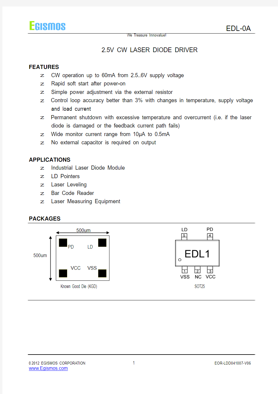
PACKAGES
500um
500um
Known Good Die (KGD) SOT25
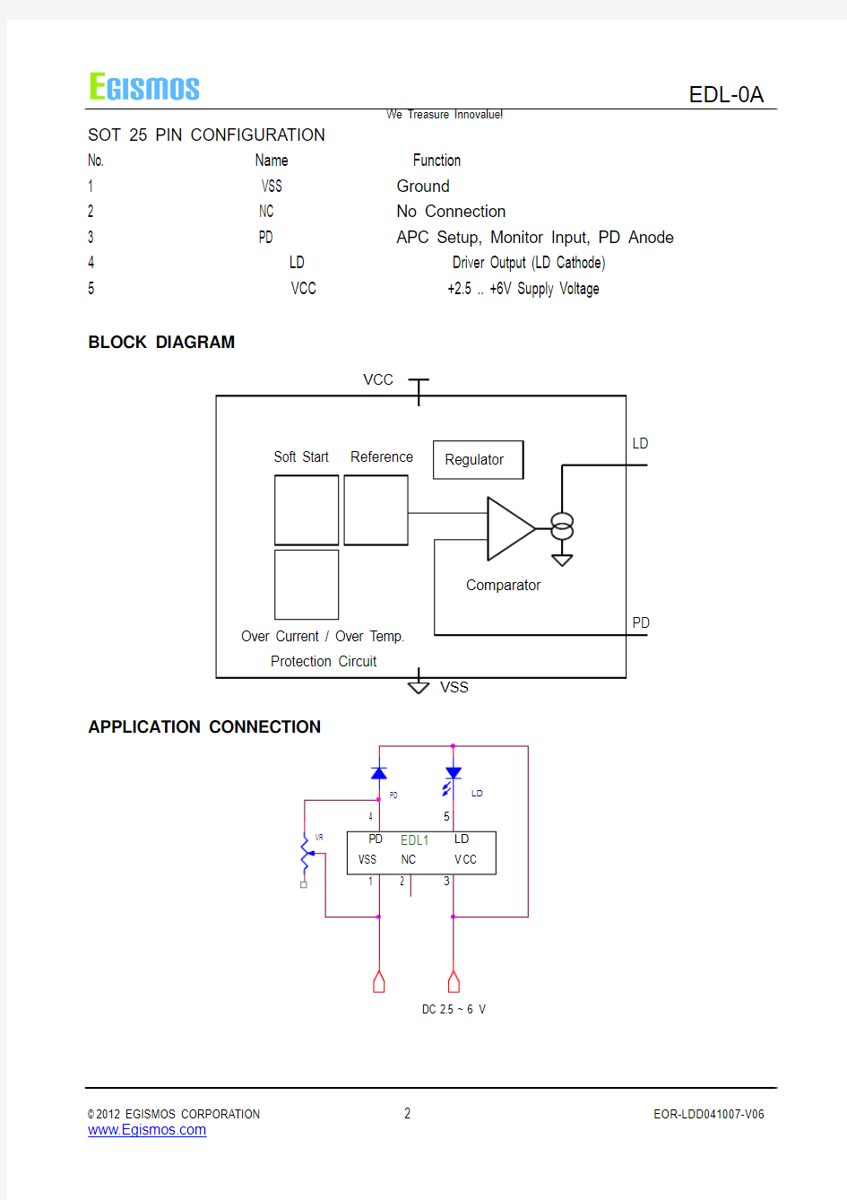
SOT 25 PIN CONFIGURATION
We Treasure Innovalue!
No. Name Function 1 VSS Ground
2 NC No Connection
3 PD APC Setup, Monitor Input, PD Anode
4 LD Driver Output (LD Cathode)
5 VCC +2.5 .. +6V Supply Voltage
BLOCK DIAGRAM
APPLICATION CONNECTION
DC 2.5 ~ 6 V
DESCRIPTION
The ED-LDDWK device is a driver for laser diodes in continuous wave operation which requires only few external components. The broad power supply range of 2.5V to 6V and the integrated reverse battery protection allow for battery operation with a minimum of two cells.
The driver includes integrated circuitry protecting against destruction by ESD, excessive temperature and over current and a soft start which regulates the power and protects the laser diode when the power supply is switched on. The driver also filters the laser diode power supply for transients.
The power supply is regulated and adapted for the laser diode used by an external resistor at PD. The monitor current acts as a reference and is regulated independent of the influence of temperature and supply voltage (range: 10μA to 0.5mA). There is no external capacitor required.
In the event of failure, such as over current in the laser path with a lack of feedback, for example, a quick power lockout is activated. The shutdown continues until power is reapplied, permitting a restart. The strain on power packs and batteries is relieved and the laser class is retained even in the event of a disturbance.
ABSOLUTE MAXIMUM RATINGS
Beyond these values damage may occur; device operation is not guaranteed.
THERMAL DATA
All voltages are referenced to ground unless otherwise noted.
All currents into the device pins are positive; all currents out of the device pins are negative.
ELECTRICAL CHARACTERISTICS
Operating Conditions: VCC= 2.5..6V, VR= 2K?..100K?, Ta= -20..80°C unless otherwise noted
LASER MODULE LAYOUT EXAMPLE
The following is a reference PCB layout design, which accommodates most of existing PCB for laser diode module. Trace must be modified to reduce EM wave emit ion, and component dimension should be altered.
SIDE A - COMPONENT SIDE B - LEA D
PD LD
EDL
1 2 3
LEA V SS
V CC
VR
D -
RESERV ED FOR SPRING
DEMO LAY O UT EXAMPLE
LEGE N D
SOLDER PA D
CONNECTING V OID
CONNECTING PA TH
SOT25 Package Drawing