General Description
Devices in the MAX3483E family (MAX3483E/MAX3485E/MAX3486E/MAX3488E/MAX3490E/MAX3491E) are ±15kV ESD-protected, +3.3V, low-power transceivers for RS-485 and RS-422 communications. Each device con-tains one driver and one receiver. The MAX3483E and MAX3488E feature slew-rate-limited drivers that minimize EMI and reduce reflections caused by improperly termi-nated cables, allowing error-free data transmission at data rates up to 250kbps. The partially slew-rate-limited MAX3486E transmits up to 2.5Mbps. The MAX3485E,MAX3490E, and MAX3491E transmit at up to 12Mbps.All devices feature enhanced electrostatic discharge (ESD) protection. All transmitter outputs and receiver inputs are protected to ±15kV using IEC 1000-4-2 Air-Gap Discharge, ±8kV using IEC 1000-4-2 Contact Discharge, and ±15kV using the Human Body Model.Drivers are short-circuit current limited and are protect-ed against excessive power dissipation by thermal shutdown circuitry that places the driver outputs into a high-impedance state. The receiver input has a fail-safe feature that guarantees a logic-high output if both inputs are open circuit.
The MAX3488E, MAX3490E, and MAX3491E feature full-duplex communication, while the MAX3483E,MAX3485E, and MAX3486E are designed for half-duplex communication.
Applications
Telecommunications
Industrial-Control Local Area Networks Transceivers for EMI-Sensitive Applications Integrated Services Digital Networks Packet Switching
Features
o ESD Protection for RS-485 I/O Pins
±15kV—Human Body Model
±8kV—IEC 1000-4-2, Contact Discharge ±15kV—IEC 1000-4-2, Air-Gap Discharge o Operate from a Single +3.3V Supply—No Charge Pump Required o Interoperable with +5V Logic o Guaranteed 12Mbps Data Rate (MAX3485E/MAX3490E/MAX3491E)
o Slew-Rate Limited for Errorless Data Transmission (MAX3483E/MAX3488E) o 2nA Low-Current Shutdown Mode
(MAX3483E/MAX3485E/MAX3486E/MAX3491E)o -7V to +12V Common-Mode Input Voltage Range o Full-Duplex and Half-Duplex Versions Available o Industry-Standard 75176 Pinout (MAX3483E/MAX3485E/MAX3486E)
o Current-Limiting and Thermal Shutdown for Driver Overload Protection
MAX3483E/MAX3485E/MAX3486E/MAX3488E/MAX3490E/MAX3491E
3.3V-Powered, ±15kV ESD-Protected, 12Mbps and Slew-Rate-Limited T rue RS-485/RS-422 T ransceivers
________________________________________________________________Maxim Integrated Products
1
19-1474; Rev 0; 4/99
Selector Guide
Ordering Information
Ordering Information continued at end of data sheet.
For free samples & the latest literature: https://www.doczj.com/doc/023153813.html,, or phone 1-800-998-8800.For small orders, phone 1-800-835-8769.
M A X 3483E /M A X 3485E /M A X 3486E /M A X 3488E /M A X 3490E /M A X 3491E
3.3V-Powered, ±15kV ESD-Protected, 12Mbps and Slew-Rate-Limited T rue RS-485/RS-422 T ransceivers
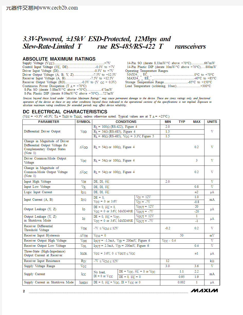
ABSOLUTE MAXIMUM RATINGS
DC ELECTRICAL CHARACTERISTICS
(V = +3.3V ±0.3V, T = T to T , unless otherwise noted. Typical values are at T = +25°C.)
Stresses beyond those listed under “Absolute Maximum Ratings” may cause permanent damage to the device. These are stress ratings only, and functional operation of the device at these or any other conditions beyond those indicated in the operational sections of the specifications is not implied. Exposure to absolute maximum rating conditions for extended periods may affect device reliability.
Supply Voltage (V CC ).............................................................+7V Control Input Voltage (RE , DE).................................-0.3V to +7V Driver Input Voltage (DI)...........................................-0.3V to +7V Driver Output Voltage (A, B, Y, Z).......................-7.5V to +12.5V Receiver Input Voltage (A, B)..............................-7.5V to +12.5V Receiver Output Voltage (RO)....................-0.3V to (V CC + 0.3V)Continuous Power Dissipation (T A = +70°C)
8-Pin SO (derate 5.88mW/°C above +70°C)..................471mW 8-Pin Plastic DIP (derate 9.09mW/°C above +70°C).....727mW
14-Pin SO (derate 8.33mW/°C above +70°C)................667mW 14-Pin Plastic DIP (derate 10mW/°C above +70°C)......800mW Operating Temperature Ranges
MAX34_ _ EC_ _...................................................0°C to +70°C MAX34_ _ EE_ _.................................................-40°C to +85°C Storage Temperature Range.............................-65°C to +150°C Lead Temperature (soldering, 10sec).............................+300°C
MAX3483E/MAX3485E/MAX3486E/MAX3488E/MAX3490E/MAX3491E
3.3V-Powered, ±15kV ESD-Protected, 12Mbps and Slew-Rate-Limited T rue RS-485/RS-422 T ransceivers
DC ELECTRICAL CHARACTERISTICS (continued)
(V CC = +3.3V ±0.3V, T A = T MIN to T MAX , unless otherwise noted. Typical values are at T A = +25°C.)
DRIVER SWITCHING CHARACTERISTICS—MAX3485E/MAX3490E/MAX3491E
(V = +3.3V, T = +25°C.)
DRIVER SWITCHING CHARACTERISTICS—MAX3486E
(V = +3.3V, T = +25°C.)
*MAX3488E and MAX3491E will be compliant to ±8kV per IEC 1000-4-2 Contact Discharge by September 1999.
M A X 3483E /M A X 3485E /M A X 3486E /M A X 3488E /M A X 3490E /M A X 3491E
3.3V-Powered, ±15kV ESD-Protected, 12Mbps and Slew-Rate-Limited T rue RS-485/RS-422 T ransceivers
4
_______________________________________________________________________________________
DRIVER SWITCHING CHARACTERISTICS—MAX3483E/MAX3488E
(V CC = +3.3V, T A = +25°C.)
RECEIVER SWITCHING CHARACTERISTICS
(V CC = +3.3V, T A = +25°C.)
Note 1:?V OD and ?V OC are the changes in V OD and V OC , respectively, when the DI input changes state.Note 2:Measured on |t PLH (Y) - t PHL (Y)|and |t PLH (Z) - t PHL (Z)|.
Note 3:The transceivers are put into shutdown by bringing RE high and DE low. If the inputs are in this state for less than 80ns, the
devices are guaranteed not to enter shutdown. If the inputs are in this state for at least 300ns, the devices are guaranteed to have entered shutdown. See Low-Power Shutdown Mode section.
MAX3483E/MAX3485E/MAX3486E/MAX3488E/MAX3490E/MAX3491E
3.3V-Powered, ±15kV ESD-Protected, 12Mbps and Slew-Rate-Limited T rue RS-485/RS-422 T ransceivers
_______________________________________________________________________________________5
Typical Operating Characteristics
(V CC = +3.3V, T A = +25°C, unless otherwise noted.)
25201510
5
00
0.5
1.0
1.5
2.0
2.5
3.5
3.0
OUTPUT CURRENT vs.
RECEIVER OUTPUT LOW VOLTAGE
M A X 3483E -01
OUTPUT LOW VOLTAGE (V)
O U T P U T C U R R E N T (m A )
-20-18-16-14-12-10-8-6-4-2
00
0.5
1.0
1.5
2.0
2.5
3.5
3.0
OUTPUT CURRENT vs.
RECEIVER OUTPUT HIGH VOLTAGE
M A X 3483E -02
OUTPUT HIGH VOLTAGE (V)
O U T P U T C U R R E N T (m A )
3.00
3.053.103.153.203.253.30-40-200204060100
80RECEIVER OUTPUT HIGH VOLTAGE
vs. TEMPERATURE
TEMPERATURE (°C)
O U T P U T H I G H V O L T A G E (V )
00.10.20.30.40.50.60.70.8-40
-20
20
40
6010080
RECEIVER OUTPUT LOW VOLTAGE
vs. TEMPERATURE
TEMPERATURE (°C)O U T P U T L O W V O L T A G E (V )
25050751001251501750
2
4
6
8
10
12
OUTPUT CURRENT vs.DRIVER OUTPUT LOW VOLTAGE
M A X 3483E -07
OUTPUT LOW VOLTAGE (V)
O U T P U T C U R R E N T (m A )
1009080706050403020100
00.5 1.0 1.5 2.0 2.5 3.53.0DRIVER OUTPUT CURRENT vs.DIFFERENTIAL OUTPUT VOLTAGE
M A X 3483E -05
DIFFERENTIAL OUTPUT VOLTAGE (V)O U T P U T C U R R E N T (m A )
1.6
1.71.81.9
2.02.12.22.32.42.6
2.5-40-200204060100
80DRIVER DIFFERENTIAL OUTPUT VOLTAGE vs. TEMPERATURE
TEMPERATURE (°C)
D I F F
E R E N T I A L O U T P U T V O L T A G E (V )
-100
-80-60
-40
-205
4
3
210-7-6-3-4-5-2-1OUTPUT CURRENT vs.DRIVER OUTPUT HIGH VOLTAGE
M A X 3483E -08
OUTPUT HIGH VOLTAGE (V)
O U T P U T C U R R E N T (m A )
M A X 3483E /M A X 3485E /M A X 3486E /M A X 3488E /M A X 3490E /M A X 3491E
3.3V-Powered, ±15kV ESD-Protected, 12Mbps and Slew-Rate-Limited T rue RS-485/RS-422 T ransceivers
0.80.70.9
1.0
1.11.2-40
-20
20
40
60
100
80
SUPPLY CURRENT vs. TEMPERATURE
TEMPERATURE (°C)
S U P P L Y C U R R E N T (m A )
Typical Operating Characteristics (continued)
(V CC = +3.3V, T A = +25°C, unless otherwise noted.)
010
20304050607080100
90-40
-20
20
40
60
100
80
SHUTDOWN CURRENT vs. TEMPERATURE
M A X 3483E -10
TEMPERATURE (°C)
S H U T D O W N C U R R E N T (n A )
Pin Description
MAX3483E/MAX3485E/MAX3486E/MAX3488E/MAX3490E/MAX3491E
3.3V-Powered, ±15kV ESD-Protected, 12Mbps and Slew-Rate-Limited T rue RS-485/RS-422 T ransceivers
_______________________________________________________________________________________
7
Figure 2. MAX3488E/MAX3490E Pin Configuration and Typical Operating Circuit
Figure 3. MAX3491E Pin Configuration and Typical Operating Circuit
Figure 1. MAX3483E/MAX3485E/MAX3486E Pin Configuration and Typical Operating Circuit
M A X 3483E /M A X 3485E /M A X 3486E /M A X 3488E /M A X 3490E /M A X 3491E
3.3V-Powered, ±15kV ESD-Protected, 12Mbps and Slew-Rate-Limited T rue RS-485/RS-422 T ransceivers
8_______________________________________________________________________________________
Figure 4. Driver V OD and V OC Figure 7. Driver Differential Output Delay and Transition Times
Figure 6. Receiver V OH and V OL
Figure 5. Driver V OD with Varying Common-Mode Voltage
MAX3483E/MAX3485E/MAX3486E/MAX3488E/MAX3490E/MAX3491E
3.3V-Powered, ±15kV ESD-Protected, 12Mbps and Slew-Rate-Limited T rue RS-485/RS-422 T ransceivers
_______________________________________________________________________________________9
Figure 8. Driver Propagation Times
Figure 9. Driver Enable and Disable Times (t PZH , t PSH , t PHZ )
Figure 10. Driver Enable and Disable Times (t PZL , t PSL , t PLZ )
M A X 3483E /M A X 3485E /M A X 3486E /M A X 3488E /M A X 3490E /M A X 3491E
3.3V-Powered, ±15kV ESD-Protected, 12Mbps and Slew-Rate-Limited T rue RS-485/RS-422 T ransceivers
10______________________________________________________________________________________
Figure 11. Receiver Propagation Delay
Figure 12. Receiver Enable and Disable Times
Note 4: The input pulse is supplied by a generator with the following characteristics: f = 250kHz, 50% duty cycle, t r ≤6.0ns, Z O = 50?.Note 5: C L includes probe and stray capacitance.
_____________________Function Tables
Devices with Receiver/Driver Enable
(MAX3483E/MAX3485E/MAX3486E/MAX3491E)
Table 1. Transmitting
* B and A outputs are Z and Y, respectively, for full-duplex part (MAX3491E).
X = Don’t care; High-Z = High impedance
Table 2. Receiving
* DE is a “don’t care” (x) for the full-duplex part (MAX3491E).X = Don’t care; High-Z = High impedance
Devices without Receiver/Driver Enable
(MAX3488E/MAX3490E)
Table 3. Transmitting
Table 4. Receiving
___________Applications Information
The MAX3483E/MAX3485E/MAX3486E/MAX3488E/MAX3490E/MAX3491E are low-power transceivers for RS-485 and RS-422 communications. The MAX3483E and MAX3488E can transmit and receive at data rates up to 250kbps, the MAX3486E at up to 2.5Mbps, and the MAX3485E/MAX3490E/MAX3491E at up to 12Mbps. The MAX3488E/MAX3490E/MAX3491E are full-duplex trans-ceivers, while the MAX3483E/MAX3485E/MAX3486E are half-duplex. Driver Enable (DE) and Receiver Enable (RE ) pins are included on the MAX3483E/MAX3485E/MAX3486E/MAX3491E. When disabled, the driver and receiver outputs are high impedance.
Reduced EMI and Reflections (MAX3483E/MAX3486E/MAX3488E)
The MAX3483E/MAX3488E are slew-rate limited, mini-mizing EMI and reducing reflections caused by improp-erly terminated cables. Figure 13 shows the driver output waveform of a MAX3485E/MAX3490E/MAX3491E transmitting a 125kHz signal, as well as the Fourier analysis of that waveform. High-frequency harmonics with large amplitudes are evident. Figure 14 shows the same information, but for the slew-rate-limited MAX3483E/MAX3488E transmitting the same signal. The high-frequency harmonics have much lower amplitudes,and the potential for EMI is significantly reduced.
Low-Power Shutdown Mode
(MAX3483E/MAX3485E/MAX3486E/MAX3491E)
A low-power shutdown mode is initiated by bringing both RE high and DE low. The devices will not shut down unless both the driver and receiver are disabled (high impedance). In shutdown, the devices typically draw only 2nA of supply current.
For these devices, the t PSH and t PSL enable times assume the part was in the low-power shutdown mode;the t PZH and t PZL enable times assume the receiver or driver was disabled, but the part was not shut down.
MAX3483E/MAX3485E/MAX3486E/MAX3488E/MAX3490E/MAX3491E
3.3V-Powered, ±15kV ESD-Protected, 12Mbps and Slew-Rate-Limited T rue RS-485/RS-422 T ransceivers
______________________________________________________________________________________
11
INPUTS OUTPUT A, B RO ≥+0.2V 1≤-0.2V 0Inputs Open
1
INPUT OUTPUTS DI Z Y 1010
1
5MHz 500kHz/div 05MHz
500kHz/div Figure 13. Driver Output Waveform and FFT Plot of MAX3485E/MAX3490E/MAX3491E Transmitting a 125kHz Signal Figure 14. Driver Output Waveform and FFT Plot of MAX3483E/ MAX3488E Transmitting a 125kHz Signal
M A X 3483E /M A X 3485E /M A X 3486E /M A X 3488E /M A X 3490E /M A X 3491E
3.3V-Powered, ±15kV ESD-Protected, 12Mbps and Slew-Rate-Limited T rue RS-485/RS-422 T ransceivers
12______________________________________________________________________________________
Figure 17. MAX3483E/MAX3488E Driver Propagation Delay Figure 19. MAX3483E/MAX3488E System Differential Voltage at 125kHz Driving 4000 Feet of Cable Figure 20. MAX3485E/MAX3490E/MAX3491E System Differential Voltage at 125kHz Driving 4000 Feet of Cable
Driver-Output Protection Excessive output current and power dissipation caused by faults or by bus contention are prevented by two mechanisms. A foldback current limit on the output stage provides immediate protection against short circuits over the whole common-mode voltage range (see Typical Operating Characteristics). In addition, a thermal shut-down circuit forces the driver outputs into a high-imped-ance state if the die temperature rises excessively.
Propagation Delay Figures 15–18 show the typical propagation delays. Skew time is simply the difference between the low-to-high and high-to-low propagation delay. Small driver/receiver skew times help maintain a symmetrical mark-space ratio (50% duty cycle).
The receiver skew time, |t PRLH- t PRHL|, is under 10ns (20ns for the MAX3483E/MAX3488E). The driver skew times are 8ns for the MAX3485E/MAX3490E/MAX3491E, 12ns for the MAX3486E, and typically under 50ns for the MAX3483E/MAX3488E.
Line Length vs. Data Rate The RS-485/RS-422 standard covers line lengths up to 4000 feet. For line lengths greater than 4000 feet, see Figure 21 for an example of a line repeater.
Figures 19 and 20 show the system differential voltage for parts driving 4000 feet of 26AWG twisted-pair wire at 125kHz into 120?loads.
For faster data rate transmission, please consult the fac-tory.
±15kV ESD Protection As with all Maxim devices, ESD-protection structures are incorporated on all pins to protect against electrostatic discharges encountered during handling and assembly. The driver outputs and receiver inputs of the MAX3483E family of devices have extra protection against static electricity. Maxim’s engineers have developed state-of-the-art structures to protect these pins against ESD of ±15kV without damage. The ESD structures withstand high ESD in all states: normal operation, shutdown, and powered down. After an ESD event, Maxim’s E versions keep working without latchup or damage.
ESD protection can be tested in various ways; the transmitter outputs and receiver inputs of this product family are characterized for protection to the following limits:
1)±15kV using the Human Body Model
2)±8kV using the Contact-Discharge method specified
in IEC 1000-4-2
3)±15kV using IEC 1000-4-2’s Air-Gap method.
ESD Test Conditions ESD performance depends on a variety of conditions. Contact Maxim for a reliability report that documents test setup, test methodology, and test results.
Human Body Model Figure 22a shows the Human Body Model and Figure 22b shows the current waveform it generates when dis-charged into a low impedance. This model consists of a 100pF capacitor charged to the ESD voltage of inter-est, which is then discharged into the test device through a 1.5k?resistor.
IEC 1000-4-2 The IEC 1000-4-2 standard covers ESD testing and performance of finished equipment; it does not specifi-cally refer to integrated circuits. The MAX3483E family of devices helps you design equipment that meets Level 4 (the highest level) of IEC 1000-4-2, without the need for additional ESD-protection components.
The major difference between tests done using the Human Body Model and IEC 1000-4-2 is higher peak current in IEC 1000-4-2, because series resistance is lower in the IEC 1000-4-2 model. Hence, the ESD with-stand voltage measured to IEC 1000-4-2 is generally lower than that measured using the Human Body Model. Figure 23a shows the IEC 1000-4-2 model, and Figure 23b shows the current waveform for the ±8kV IEC 1000-4-2, Level 4 ESD contact-discharge test.
Figure 21. Line Repeater for MAX3488E/MAX3490E/MAX3491E
MAX3483E/MAX3485E/MAX3486E/MAX3488E/MAX3490E/MAX3491E3.3V-Powered, ±15kV ESD-Protected, 12Mbps and Slew-Rate-Limited T rue RS-485/RS-422 T ransceivers ______________________________________________________________________________________13
M A X 3483E /M A X 3485E /M A X 3486E /M A X 3488E /M A X 3490E /M A X 3491E
The air-gap test involves approaching the device with a charged probe. The contact-discharge method connects the probe to the device before the probe is energized.
Machine Model
The Machine Model for ESD tests all pins using a 200pF storage capacitor and zero discharge resis-tance. Its objective is to emulate the stress caused when I/O pins are contacted by handling equipment during test and assembly. Of course, all pins require this protection, not just RS-485 inputs and outputs.
Typical Applications
The MAX3483E/MAX3485E/MAX3486E/MAX3488E/MAX3490E/MAX3491E transceivers are designed for bidirectional data communications on multipoint bus transmission lines. Figures 24 and 25 show typical net-work applications circuits. These parts can also be used as line repeaters, with cable lengths longer than 4000 feet, as shown in Figure 21.
To minimize reflections, the line should be terminated at both ends in its characteristic impedance, and stub lengths off the main line should be kept as short as possible. The slew-rate-limited MAX3483E/MAX3488E and the partially slew-rate-limited MAX3486E are more tolerant of imperfect termination.
3.3V-Powered, ±15kV ESD-Protected, 12Mbps and Slew-Rate-Limited T rue RS-485/RS-422 T ransceivers
14______________________________________________________________________________________
Figure 22a. Human Body ESD Test Model
Figure 22b. Human Body Current Waveform
Figure 23a. IEC 1000-4-2 ESD Test Model
Figure 23b. IEC 1000-4-2 ESD Generator Current Waveform
MAX3483E/MAX3485E/MAX3486E/MAX3488E/MAX3490E/MAX3491E
3.3V-Powered, ±15kV ESD-Protected, 12Mbps and Slew-Rate-Limited T rue RS-485/RS-422 T ransceivers
______________________________________________________________________________________15
Figure 25. MAX3488E/MAX3490E/MAX3491E Full-Duplex RS-485 Network
Figure 24. MAX3483E/MAX3485E/MAX3486E Typical RS-485 Network
M A X 3483E /M A X 3485E /M A X 3486E /M A X 3488E /M A X 3490E /M A X 3491E
3.3V-Powered, ±15kV ESD-Protected, 12Mbps and Slew-Rate-Limited T rue RS-485/RS-422 T ransceivers
TRANSISTOR COUNT: 761
Chip Information
Ordering Information (continued)
Maxim cannot assume responsibility for use of any circuitry other than circuitry entirely embodied in a Maxim product. No circuit patent licenses are implied. Maxim reserves the right to change the circuitry and specifications without notice at any time.
16____________________Maxim Integrated Products, 120 San Gabriel Drive, Sunnyvale, CA 94086 408-737-7600?1999 Maxim Integrated Products
Printed USA
is a registered trademark of Maxim Integrated Products.