IRLR/U120NPbF
HEXFET ?
Power MOSFET
Description
12/6/04
Parameter
Max.
Units
I D @ T C = 25°C Continuous Drain Current, V GS @ 10V 10I D @ T C = 100°C Continuous Drain Current, V GS @ 10V 7.0A I DM
Pulsed Drain Current 35P D @T C = 25°C Power Dissipation 48W Linear Derating Factor 0.32W/°C V GS Gate-to-Source Voltage
± 16V E AS Single Pulse Avalanche Energy 85mJ I AR Avalanche Current
6.0A E AR Repetitive Avalanche Energy 4.8mJ dv/dt Peak Diode Recovery dv/dt 5.0
V/ns T J Operating Junction and
-55 to + 175T STG
Storage Temperature Range
Soldering Temperature, for 10 seconds
300 (1.6mm from case )
°C
Absolute Maximum Ratings
Parameter
Typ.
Max.
Units
R θJC Junction-to-Case
––– 3.1R θJA Junction-to-Ambient (PCB mount) **–––50°C/W
R θJA
Junction-to-Ambient
–––
110
Thermal Resistance
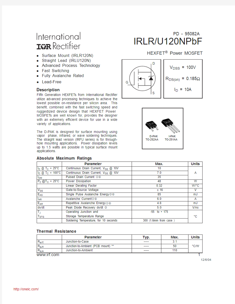
D-PAK TO-252AA I-PAK TO-251AA
l Surface Mount (IRLR120N)l Straight Lead (IRLU120N)
l Advanced Process Technology l Fast Switching
l Fully Avalanche Rated Fifth Generation HEXFETs from International Rectifier utilize advanced processing techniques to achieve the lowest possible on-resistance per silicon area. This benefit, combined with the fast switching speed and ruggedized device design that HEXFET Power MOSFETs are well known for, provides the designer with an extremely efficient device for use in a wide variety of applications.
The D-PAK is designed for surface mounting using vapor phase, infrared, or wave soldering techniques.The straight lead version (IRFU series) is for through-hole mounting applications. Power dissipation levels up to 1.5 watts are possible in typical surface mount applications.
PD - 95082A
https://www.doczj.com/doc/012444770.html, 1
l
Lead-Free
IRLR/U120NPbF
https://www.doczj.com/doc/012444770.html,
Electrical Characteristics @ T = 25°C (unless otherwise specified)
Notes:
V DD = 25V, starting T J = 25°C, L = 4.7mH R G = 25?, I AS = 6.0A. (See Figure 12) Repetitive rating; pulse width limited by max. junction temperature. ( See fig. 11 ) ** When mounted on 1" square PCB (FR-4 or G-10 Material ) .
For recommended footprint and soldering techniques refer to application note #AN-994
I SD ≤ 6.0A, di/dt ≤ 340A/μs, V DD ≤ V (BR)DSS , T J ≤ 175°C
Uses IRL520N data and test conditions.
This is applied for I-PAK, L S of D-PAK is measured between lead and
center of die contact
Pulse width ≤ 300μs; duty cycle ≤ 2%.
IRLR/U120NPbF
https://www.doczj.com/doc/012444770.html, 3
Fig 3. Typical Transfer Characteristics
Fig 4. Normalized On-Resistance
Vs. Temperature
Fig 1. Typical Output Characteristics Fig 2. Typical Output Characteristics
and
0.1
1
10
1000.1
1
10
100
I , D r a i n -t o -S o u r c e C u r r e n t (A )
D V , Drain-to-Source Voltage (V)DS
0.1
1
10
1000.1
1
10
100
I , D r a i n -t o -S o u r c e C u r r e n t (A )
D V , Drain-to-Source Voltage (V)DS
0.1
110
1002
4
6
8
10
GS V , Gate-to-Source Voltage (V)D I , D r a i n -t o -S o u r c e C u r r e n t (A )
0.0
0.5
1.0
1.5
2.0
2.5
3.0
-60-40-20
20
40
60
80100120140160180
J
T , Junction Temperature (°C)R , D r a i n
-t o -S o u r c e O n R e s i s t a n c e D S (o n
)(N o r m a l i z e d )
IRLR/U120NPbF
https://www.doczj.com/doc/012444770.html,
Fig 8. Maximum Safe Operating Area
Fig 6. Typical Gate Charge Vs.
Gate-to-Source Voltage
Fig 5. Typical Capacitance Vs.Drain-to-Source Voltage Fig 7. Typical Source-Drain Diode Forward Voltage
0200
400
600
800
1
10
100
C , C a p a c i t a n c e (p F )
DS
V , Drain-to-Source Voltage (V)
03
6
9
12
15
5
10
15
20
25
Q , Total Gate Charge (nC)G
V , G a t e -t o -S o u r c e V o l t a g e (V )
G S
0.11
10
1000.4
0.6
0.8
1.0
1.2
1.4
V , Source-to-Drain Voltage (V)I , R e v e r s e D r a i n C u r r e n t (A )
SD
S D 0.1
1
10
100
1
10
100
1000
V , Drain-to-Source Voltage (V)
DS
I , D r a i n C u r r e n t (A )D
IRLR/U120NPbF
https://www.doczj.com/doc/012444770.html, 5
Fig 9. Maximum Drain Current Vs.Case Temperature
Fig 10a.
Switching Time Test Circuit
V V d(on)
r
d(off)
f
Fig 10b. Switching Time Waveforms
V DD
2
4
6
8
10
25
50
75
100
125
150
175
C
I , D r a i n C u r r e n t (A m p s )
D T , Case Temperature (°C)
IRLR/U120NPbF
6
https://www.doczj.com/doc/012444770.html,
V 5.0 V
Fig 13b. Gate Charge Test Circuit
Fig 13a. Basic Gate Charge Waveform Fig 12c. Maximum Avalanche Energy
Vs. Drain Current
DS
Current Sampling Resistors
Fig 12b. Unclamped Inductive Waveforms
Fig 12a. Unclamped Inductive Test Circuit
I AS
V DD
040
80
120
160
200
25
50
75
100
125
150
175
J
E , S i n
g l e P u l s e A v a l a n c h e E n e r g y (m J )A
S Starting T , Junction Temperature (°C)
IRLR/U120NPbF
https://www.doczj.com/doc/012444770.html, 7
Fig 14. For N-Channel HEXFETS
* V GS = 5V for Logic Level Devices
Peak Diode Recovery dv/dt Test Circuit
V DD
I-Pak (TO-251AA) Package Outline Dimensions are shown in millimeters (inches)
IRLR/U120NPbF
https://www.doczj.com/doc/012444770.html,
Data and specifications subject to change without notice.
IR WORLD HEADQUARTERS: 233 Kansas St., El Segundo, California 90245, USA Tel: (310) 252-7105
TAC Fax: (310) 252-7903
Visit us at https://www.doczj.com/doc/012444770.html, for sales contact information .12/04
D-Pak (TO-252AA) Tape & Reel Information
Dimensions are shown in millimeters (inches)
TR
16.3 ( .641 )15.7 ( .619 )8.1 ( .318 )7.9 ( .312 )
12.1 ( .476 )11.9 ( .469 )
FEED DIRECTION
FEED DIRECTION
16.3 ( .641 )15.7 ( .619 )
TRR
TRL
NOTES :
1. CONTROLLING DIMENSION : MILLIMETER.
2. ALL DIMENSIONS ARE SHOWN IN MILLIMETERS ( INCHES ).
3. OUTLINE CONFORMS TO EIA-481 & EIA-541.
NOTES :
1. OUTLINE CONFORMS TO EIA-481.
16 mm
13 INCH
分销商库存信息:
IR
IRLU120NPBF IRLR120NTRPBF IRLR120NTRLPBF IRLR120NPBF